Äîêóìåíòàöèÿ è îïèñàíèÿ www.docs.chipfind.ru
a
MicroConverter, Dual 16-Bit ADCs
with Embedded 62kB FLASH MCU
Preliminary Technical Data
ADuC846
PRELIMINARY TECHNICAL DATA
REV. PrA
Information furnished by Analog Devices is believed to be accurate and reliable.
However, no responsibility is assumed by Analog Devices for its use, nor for any
infringements of patents or other rights of third parties that may result from its use.
No license is granted by implication or otherwise under any patent or patent rights
One Technology Way, P.O. Box 9106, Norwood, MA 02062-9106, U.S.A.
Tel: 781/329-4700
www.analog.com
FEATURES
High Resolution Sigma-Delta ADCs
Two Independent ADCs (16-Bit Resolution)
16-Bit No Missing Codes
16-Bit rms (16 Bit p-p) Effective Resolution @ 20 Hz
Offset Drift 10 nV/°C, Gain Drift 0.5 ppm/°C
Memory
62 Kbytes On-Chip Flash/EE Program Memory
4 Kbytes On-Chip Flash/EE Data Memory
Flash/EE, 100 Year Retention, 100 Kcycles Endurance
3 Levels of Flash/EE Program Memory Security
In-Circuit Serial Download (No External Hardware)
High Speed User Download (5 Seconds)
2304 Bytes On-Chip Data RAM
8051-Based Core
8051 Compatible Instruction Set
High Performance Single Cycle Core
32 kHz External Crystal
On-Chip Programmable PLL (12.58 MHz Max)
3
× 16-Bit Timer/Counter
26 Programmable I/O Lines
11 Interrupt Sources, Two Priority Levels
Dual Data Pointer, Extended 11-Bit Stack Pointer
On-Chip Peripherals
Internal Power on Reset Circuit
12-Bit Voltage Output DAC
Dual 16-Bit S-D DACs/PWMs
On-Chip Temperature Sensor
Dual Excitation Current Sources
Time Interval Counter (Wakeup/RTC Timer)
UART, SPI®, and I2C® Serial I/O
High Speed Baud Rate Generator (incl 115,200)
Watchdog Timer (WDT)
Power Supply Monitor (PSM)
Power
Normal: 2.3mA Max @ 3.6 V (Core CLK = 1.57 MHz)
Power-Down: 20
µA Max with Wakeup Timer Running
Specified for 3 V and 5 V Operation
Package and Temperature Range
52-Lead MQFP (14 mm
× 14 mm), 40°C to +125°C
56-Lead CSP (8 mm
× 8 mm), 40°C to +85°C
APPLICATIONS
Intelligent Sensors
WeighScales
Portable Instrumentation, Battery Powered Systems
4-20mA Transmitters
Data Logging
Precision System Monitoring
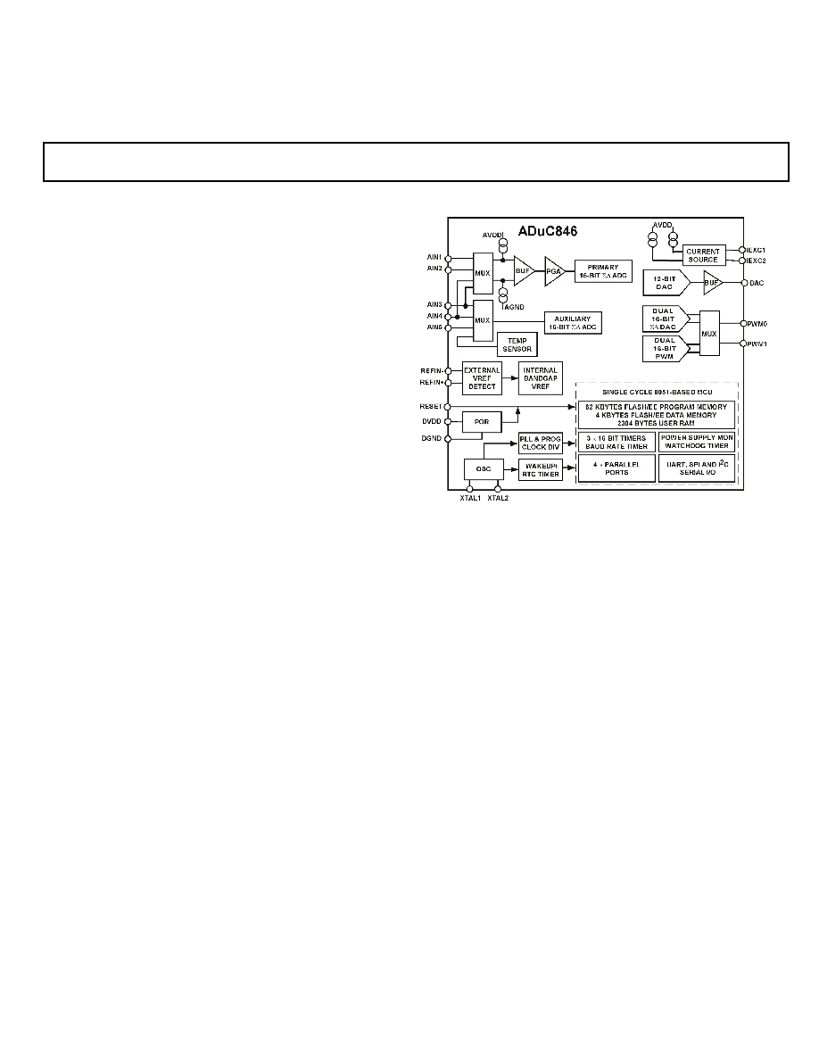
FUNCTIONAL BLOCK DIAGRAM
GENERAL DESCRIPTION
The ADuC846 is a complete smart transducer front end, integrating
two high resolution sigma-delta ADCs, an 8-bit MCU, and
program/data Flash/EE memory on a single chip.
The two independent ADCs (primary and auxiliary) include a
temperature sensor and a PGA (allowing direct measurement of low
level signals). The ADCs with on-chip digital filtering and
programmable output data rates are intended for the measurement of
wide dynamic range, low frequency signals, such as those in weigh
scale, strain-gage, pressure transducer, or temperature measurement
applications.
The device operates from a 32 kHz crystal with an on-chip PLL
generating a high frequency clock of 12.58 MHz. This clock is routed
through a programmable clock divider from which the MCU core
clock operating frequency is generated. The microcontroller core is an
optimized single cycle 8052 offering up to 12.58MIPs performance
while maintaining the 8051 instruction set compatibility.
62 Kbytes of nonvolatile Flash/EE program memory, 4 Kbytes of
nonvolatile Flash/EE data memory, and 2304 bytes of data RAM are
provided on-chip. The program memory can be configured as data
memory to give up to 60 Kbytes of NV data memory in data logging
applications.
On-chip factory firmware supports in-circuit serial download and
debug modes (via UART), as well as single-pin emulation mode via
the EA pin. The ADuC846 is supported by a QuickStartTM
development system featuring low cost software and hardware
development tools.
of Analog Devices. Trademarks and registered trademarks are the property of
their respective companies.
Fax: 781/326-8703
© 2003 Analog Devices, Inc. All rights reserved.

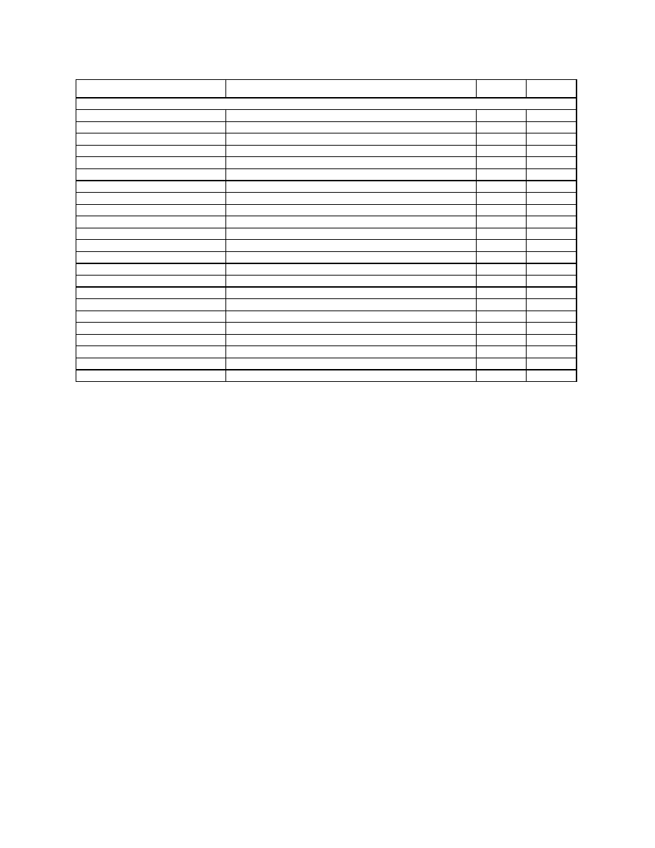
SPECIFICATIONS
1
PRELIMINARY TECHNICAL DATA
(AVDD = 2.7 V to 3.6 V or 4.75 V to 5.25 V, DVDD = 2.7 V to 3.6 V or 4.75 V to 5.25 V, REFIN(+)
= 2.5 V, REFIN() = AGND; AGND = DGND = 0 V; XTAL1/XTAL2 = 32.768 kHz Crystal; all
specifications T
MIN
, to T
MAX
unless otherwise noted.).
PARAMETER MIN
TYP
MAX
UNITS
CONDITION
PRIMARY ADC
Conversion
Rate
5.35 19.79 105
Hz
On Both Channels
No Missing Codes
2
16
Bits
19.79Hz Update Rate
Resolution
13.5
Bits
Pk-Pk Range = ± 20mV, 20Hz Update Rate
16
Bits Pk-Pk
Range = ± 2.56V, 20Hz Update Rate
Output Noise
See Tables X and XI in
ADuC836 Datasheet
Output Noise varies with selected Update Rates
and Gain Range
Integral Non Linearity
± 15
ppm of FSR 1 LSB
16
Offset
Error
3
±
3
µV
Offset Error Drift (vs. Temp)
± 10
nV/°C
Full-Scale
Error
4
±
10
µV
Gain Error Drift
5
(vs. Temp)
± 0.5
ppm/°C
ADC Range Matching
± 2
µV
AIN=18mV
Power Supply Rejection
80
dBs
AIN=1V, Range=± 2.56V
113
dBs
AIN=7.8mV, Range=± 20mV
Common Mode DC Rejection
On AIN
95
dBs
@DC, AIN=7.8mV, Range=± 20mV
On AIN
113
dBs
@DC, AIN=1V, Range=± 2.56V
Common Mode 50/60Hz Rejection
20 Hz Update Rate
On AIN
95
dBs
50/60Hz ± 1Hz, AIN=7.8mV, Range=± 20mV
On AIN
90
dBs
50/60Hz ± 1Hz, AIN=1V, Range=± 2.56V
Normal Mode 50/60 Hz Rejection
On AIN
60
dBs
50/60Hz ± 1Hz, 20 Hz Update Rate
PRIMARY ADC ANALOG INPUTS
Differential Input Voltage Ranges
9,10
Bipolar Mode (ADC0CON.5 = 0)
± 1.024 x V
REF
/GAIN
V
V
REF
= REFIN(+) - REFIN(-) (or Int 1.25V Ref)
GAIN = 1 to 128
Unipolar Mode (ADC0CON.5 = 1)
0 1.024 x REFIN/GAIN
V
V
REF
= REFIN(+) - REFIN(-)
GAIN=1 to 128
Analog Input Current
2
±
1
nA
T
MAX
= 85°C
±
5
nA
T
MAX
= 125°C
Analog Input Current Drift
± 5
pA/°C
T
MAX
= 85°C
±
15 pA/°C
T
MAX
= 125°C
Absolute AIN Voltage Limits
2
A
GND
+ 0.1
AV
DD
0.1
V
EXTERNAL REFERENCE INPUTS
REFIN(+) to REFIN() Range
2
1
2.5
AV
DD
V
Average Reference Input Current
+/- 1
µA/V
Both ADCs Enabled
Average Reference Input Current Drift
+/- 0.01
nA/V/°C
`NO Ext. REF' Trigger Voltage
0.3
0.65
V
NOXREF bit active if VREF<0.3V
NOXREF bit Inactive if VREF>0.65
Common Mode DC Rejection
125
dBs
@DC, AIN=1V, Range=± 2.56V
Common Mode 50/60Hz Rejection
90
dBs
50/60Hz ± 1Hz, AIN=1V, Range=± 2.56V
Normal Mode 50/60 Hz Rejection
60
dBs
50/60Hz ± 1Hz, 59.4 Hz Update Rate
-2-
REV. PrA

ADuC846
REV. PrA
-3-
PRELIMINARY TECHNICAL DATA
PARAMETER MIN
TYP
MAX
UNITS
CONDITION
AUXILIARY ADC
No Missing Codes
2
16
Bits
20 Hz Update Rate
Resolution
16
Bits Pk-Pk
Range = ± 2.5V, 20Hz Update Rate
Output Noise
See Table XII in ADuC836
Datasheet
Output Noise varies with selected Update Rates
Integral Non Linearity
± 15
ppm of FSR 1 LSB
16
Offset
Error
3
-2
LSB
Offset Error Drift
1
µV /°C
Fullscale
Error
4
-2.5 LSBs
Gain Error Drift
5
± 0.5
ppm/°C
Power Supply Rejection
80
dBs
AIN=1V, Range=± 2.56V
Normal Mode 50/60 Hz Rejection
On AIN
60
dBs
50/60Hz ± 1Hz, 19.79Hz Update Rate
On REFIN
60
dBs
50/60Hz ± 1Hz, 19.79Hz Update Rate
AUXILIARY ADC ANALOG INPUTS
Differential Input Voltage Ranges
9, 10
(Bipolar Mode ADC0CON3 = 0)
± REFIN
V
REFIN=REFIN(+)-REFIN(-) (or Int 1.25V Ref)
(Unipolar Mode ADC0CON3 = 1)
0 REFIN
V
REFIN=REFIN(+)-REFIN(-) (or Int 1.25V Ref)
Average Analog Input Current
125
nA/V
Analog Input Current Drift
± 2
pA/V/°C
Absolute AIN Voltage Limits
2, 11
A
GND
- 0.03
A
VDD
+ 0.03
V
ADC SYSTEM CALIBRATION
Full Scale Calibration Limit
+1.05 x FS
V
Zero Scale Calibration Limit
-1.05 x FS
V
Input Span
0.8 x FS
2.1 x FS
V
DAC
Voltage
Range
0 V
REF
V
DACCON.2 = 0
0
AV
DD
V
DACCON.2 = 1
Resistive
Load
10 k
From DAC Output to AGND
Capactive Load
100
pF
From DAC Output to AGND
Output
Impedance
0.5
I
SINK
50
µA
DC
Specifications
7
Resolution
12
Relative Accuracy
± 3
LSBs
Differential NonLinearity
-1
Bit
Guaranteed 12-Bit Monotonic
Offset Error
± 50
mV
Gain
Error
8
±
1
%
AV
DD
Range
±
1
%
V
REF
Range
AC
Specifications
2,7
Voltage Output Settling Time
15
us
Setling time to 1LSB of final value
Digital to Analog Glitch Energy
10
nVs
1 LSB change at major carry

ADuC846 SPECIFICATIONS
1
-4-
REV. PrA
PRELIMINARY TECHNICAL DATA
PARAMETER MIN
TYP
MAX
UNITS
CONDITION
INT
REFERENCE
ADC
Reference
Reference
Voltage
1.237 1.25 1.2625
V
initial tolerance @ 25°C, VDD=5V
Power Supply Rejection
45
dBs
Reference
Tempco
100
ppm/°C
DAC
Reference
Reference
Voltage
2.475 2.5 1.525
V
initial tolerance @ 25°C, VDD=5V
Power Supply Rejection
50
dBs
Reference Tempco
± 100
ppm/°C
TEMPERATURE SENSOR
Accuracy
+/-
2
°C
Thermal Impedance
90
°C/W
MQFP Package
52
°C/W
CSP
Package
TRANSDUCER BURNOUT CURRENT SOURCES
AIN+ Current
-100
nA
AIN+ is the selected positive input to the
primary ADC
AIN- Current
100
nA
AIN- is the selected negative input to the
primary ADC
Initial Tolerance at 25°C
+/- 10
%
Drift
0.03
%/°C
EXCITATION CURRENT SOURCES
Output
Current
-200
µA
Available from each Current Source
Initial Tolerance at 25°C
+/-10
%
Drift
200
ppm/°C
Initial Current Matching at 25°C
+/-1
%
Matching between both Current Sources
Drift
Matching
20
ppm/°C
Line Regulation (AV
DD
)
1
µA/V
AV
DD
=5V +/- 5%
Load
Regulation
0.1
V
Output
Compliance
A
GND
AV
DD
-0.6 V
POWER SUPPLY MONITOR (PSM)
AV
DD
Trip Point Selection Range
2.63
4.63
V
Four Trip Points selectable in this range
AV
DD
Trip Point Accuracy
+/- 3.0
%
T
MAX
= 85°C
AV
DD
Trip Point Accuracy
+/- 3.0
%
T
MAX
= 125°C
DV
DD
Trip Point Selection Range
2.63
4.63
V
Four Trip Points selectable in this range
DV
DD
Trip Point Accuracy
+/- 3.0
%
T
MAX
= 85°C
DV
DD
Trip Point Accuracy
+/- 3.0
%
T
MAX
= 125°C
CRYSTAL OSCILLATOR (XTAL 1AND XTAL2)
Logic Inputs, XTAL1 Only
2
V
INL
, Input Low Voltage
0.8
V
DV
DD
= 5V
0.4
V
DV
DD
= 3V
V
INH
, Input Low Voltage
3.5
V
DV
DD
= 5V
2.5
V
DV
DD
= 3V
XTAL1 Input Capacitance
18
pF
XTAL2 Output Capacitance
18
pF

ADuC846
REV. PrA
-5-
PRELIMINARY TECHNICAL DATA
PARAMETER MIN
TYP
MAX
UNITS
CONDITION
LOGIC INPUTS
All Inputs except SCLOCK, RESET
and
XTAL1
2
V
INL
, Input Low Voltage
0.8
V
DV
DD
= 5V
0.4
V
DV
DD
= 3V
V
INH
, Input Low Voltage
2.0
V
SCLOCK and RESET Only
(Schmidt Triggered Inputs)
2
V
T+
1.3 3.0 V DV
DD
= 5V
0.95
2.5
V
DV
DD
= 3V
V
T-
0.8 1.4 V DV
DD
= 5V
0.4 1.1 V DV
DD
= 3V
V
T+
- V
T-
0.3
0.85
V
DV
DD
= 5V or 3V
Input
Currents
2.0
V
Port 0, P1.2 P1.7,
EA
+/-
10
µA
V
IN
= 0V or V
DD
SCLOCK,
MOSI,MISO
SS
13
-10 -40
µA
V
IN
= 0V, DV
DD
=5V, Internal Pullup
+/-10
µA
V
IN
= DV
DD
, DV
DD
=5V
RESET
+/-10
µA
V
IN
= 0V, DV
DD
=5V
35
105
µA
V
IN
= DV
DD
, DV
DD
=5V, Internal Pull-Down
P1.0, P1.1, Port 2, Port 3
+/-10
µA
V
IN
= DV
DD
, DV
DD
=5V
-180
-660
µA
V
IN
= 2V, DV
DD
=5V
-20 -75
µA
V
IN
= 0.45V, DV
DD
=5V
Input Capacitance
5
pF
All Digital Inputs
LOGIC OUTPUTS
All Digital Outputs except XTAL2
2
V
OH
, Output High Voltage
2.4
V
DV
DD
= 5V, I
SOURCE
= 80
µA
2.4
V
DV
DD
= 3V, I
SOURCE
= 20
µA
V
OL
, Output Low Voltage
14
0.8
V
I
SINK
= 8mA, SCLOCK, MOSI/SDATA
0.8
V
I
SINK
= 10mA, P1.0, P1.1
0.8
V
I
SINK
= 1.6mA, All Other Outputs
Floating State Leakage Current
+/-10
µA
Floating State Output Capacitance
5
pF
START UP TIME
At Power On
300
ms
After External RESET in Normal Mode
3
ms
After WDT RESET in Normal Mode
3
ms
Controlled via WDCON SFR
From Idle Mode
10
us
From Power-Down Mode
Oscillator Running
PLLCON.7 = 0
Wakeup with INT0 Interrupt
20
us
Wakeup with SPI Interrupt
20
us
Wakeup with TIC Interrupt
20
us
Wakeup with External RESET
3
us
Oscillator Powered Down
PLLCON.7 = 1
Wakeup with INT0 Interrupt
20
us
Wakeup with SPI Interrupt
20
us
Wakeup with External RESET
5
ms

ADuC846 SPECIFICATIONS
1
-6-
REV. PrA
PRELIMINARY TECHNICAL DATA
PARAMETER MIN
TYP
MAX
UNITS
CONDITION
FLAH/EE MEMORY RELIABILITY CHARACTERISTICS
Endurance
16
100,000 700,000
Cycles
Data
Retention
17
100
POWER REQUIREMENTS
Power Supply Voltages
AV
DD
3V Nominal
2.7
3.6
V
AV
DD
5V Nominal
4.75
5.25
V
DV
DD
3V Nominal
2.7
3.6
V
DV
DD
5V Nominal
4.75
5.25
V
5V POWER CONSUMPTION
4.75V < DVDD <5.25V, AVDD= 5.25V
Normal
Mode
18, 19
DV
DD
Current
4
mA
core clock = 1.57MHz
13
16
mA
core clock = 12.58MHz
AV
DD
Current
180
µA
Power-Down
Mode
18, 19
DV
DD
Current
53
µA
T
MAX
= 85°C; Osc ON;TIC ON
100
µA
T
MAX
= 125°C; Osc ON; TIC ON
DV
DD
Current
30
µA
T
MAX
= 85°C; Osc OFF
80
µA
T
MAX
= 125°C; Osc OFF
AV
DD
Current
1
µA
T
MAX
= 85°C; Osc ON or OFF
3
µA
T
MAX
= 125°C; Osc ON or OFF
Typical Additional Peripheral Currents (AI
DD
and D I
DD
)
Primary
ADC
1
mA
Auxiliary
ADC
0.5 mA
Power Supply Monitor
50
µA
DAC
150
µA
Dual Excitation Current Sources
400
µA
3V POWER CONSUMPTION
4.75V < DVDD <5.25V, AVDD= 5.25V
Normal
Mode
18, 19
DV
DD
Current
2.3
mA
core clock = 1.57MHz
8
10
mA
core clock = 12.58MHz
AV
DD
Current
180
µA
Power-Down
Mode
18, 19
DV
DD
Current
20
µA
T
MAX
= 85°C; Osc ON;TIC ON
40
µA
T
MAX
= 125°C; Osc ON; TIC ON
DV
DD
Current
10
µA
Osc OFF
80
µA
T
MAX
= 125°C; Osc OFF
AV
DD
Current
1
µA
T
MAX
= 85°C; Osc ON or OFF
3
µA
T
MAX
= 125°C; Osc ON or OFF

ADuC846
REV. PrA
-7-
PRELIMINARY TECHNICAL DATA
NOTES
1 Temperature Range for ADuC844BS (MQFP package) is 40°C to +125°C.
Temperature Range for ADuC844BCP (CSP package) is 40°C to +85°C.
2 These numbers are not production tested but are guaranteed by design and/or characterization data on production release.
3 System Zero-Scale Calibration can remove this error.
4 The primary ADC is factory calibrated at 25°C with AVDD = DVDD = 5 V yielding this full-scale error of 10
µ
V. If user power supply or temperature
conditions are significantly different from these, an Internal Full-Scale Calibration will restore this error to 10
µ
V. A system zero-scale and full-scale
calibration will remove this error altogether.
5 Gain Error Drift is a span drift. To calculate Full-Scale Error Drift, add the Offset Error Drift to the Gain Error Drift times the full-scale input.
6 The auxiliary ADC is factory calibrated at 25°C with AVDD = DVDD = 5 V yielding this full-scale error of 2.5 LSB. A system zero-scale and full-scale
calibration will remove this error altogether.
7 DAC linearity and ac specifications are calculated using: reduced code range of 48 to 4095, 0 to VREF, reduced code range of 100 to 3950, 0 to VDD.
8 Gain Error is a measure of the span error of the DAC.
9 In general terms, the bipolar input voltage range to the primary ADC is given by RangeADC = ±(VREF 2
RN
)/125, where:
VREF = REFIN(+) to REFIN() voltage and VREF = 1.25 V when internal ADC VREF is selected.
RN = decimal equivalent of RN2, RN1, RN0
e.g., VREF = 2.5 V and RN2, RN1, RN0 = 1, 1, 0 the RangeADC = ±1.28 V, In unipolar mode, the effective range is 0 V to 1.28 V in our example.
10 1.25 V is used as the reference voltage to the ADC when internal VREF is selected via XREF0 and XREF1 bits in ADC0CON and ADC1CON, respectively.
11 In bipolar mode, the Auxiliary ADC can only be driven to a minimum of AGND 30 mV as indicated by the Auxiliary ADC absolute AIN voltage limits. The
bipolar range is still VREF to +VREF; however, the negative voltage is limited to 30 mV.
12 The ADuC846BCP (CSP Package) has been qualified and tested with the base of the CSP Package floating.
13 Pins configured in SPI Mode, pins configured as digital inputs during this test.
14 Pins configured in I
2
C Mode only.
15 Flash/EE Memory Reliability Characteristics apply to both the Flash/EE program memory and Flash/EE data memory.
16 Endurance is qualified to 100 Kcycles as per JEDEC Std. 22 method A117 and measured at 40 °C, +25°C, +85°C, and +125°C. Typical endurance at 25°C is
700 Kcycles.
17 Retention lifetime equivalent at junction temperature (TJ) = 55°C as per JEDEC Std. 22, Method A117. Retention lifetime based on an activation energy of
0.6eV will derate with junction temperature.
18 Power Supply current consumption is measured in Normal, Idle, and Power-Down Modes under the following conditions:
Normal Mode: Reset = 0.4 V, Digital I/O pins = open circuit, Core Clk changed via CD bits in PLLCON, Core Executing internal software loop.
Idle Mode: Reset = 0.4 V, Digital I/O pins = open circuit, Core Clk changed via CD bits in PLLCON, PCON.0 = 1, Core Execution suspended in idle mode.
Power-Down Mode: Reset = 0.4 V, All P0 pins and P1.2P1.7 Pins = 0.4 V, All other digital I/O pins are open circuit, Core Clk changed via CD bits in
PLLCON, PCON.1 = 1, Core Execution suspended in power-down mode, OSC turned ON or OFF via OSC_PD bit (PLLCON.7) in PLLCON SFR.
19 DVDD power supply current will increase typically by 3 mA (3 V operation) and 10 mA (5 V operation) during a Flash/EE memory program or erase cycle.
Specifications subject to change without notice
ADuC846
-8-
REV. PrA
PRELIMINARY TECHNICAL DATA
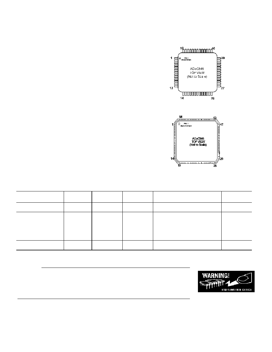
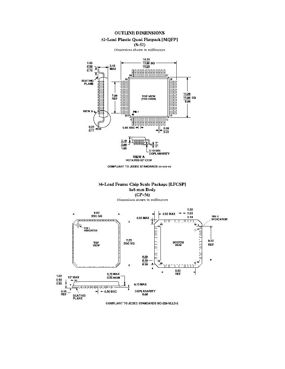
PIN CONFIGURATION
52-Lead MQFP
56-Lead CSP
ABSOLUTE MAXIMUM RATINGS
1
(TA = 25°C unless otherwise noted)
AVDD to AGND
0.3 V to +7 V
AVDD to DGND
0.3 V to +7 V
DVDD to AGND
0.3 V to +7 V
DVDD to DGND
0.3 V to +7 V
AGND to DGND2
0.3 V to +0.3 V
AVDD to DVDD
2 V to +5 V
Analog Input Voltage to AGND
3
0.3 V to AVDD +0.3 V
Reference Input Voltage to AGND
0.3 V to AVDD +0.3 V
AIN/REFIN Current (Indefinite)
30 mA
Digital Input Voltage to DGND
0.3 V to DVDD +0.3 V
Digital Output Voltage to DGND
0.3 V to DVDD +0.3 V
Operating Temperature Range
40°C to +125°C
Storage Temperature Range
65°C to +150°C
Junction Temperature
150°C
JA Thermal Impedance
90°C/W
Lead Temperature, Soldering
Vapor Phase (60 sec)
215°C
Infrared (15 sec)
220°C
1Stresses above those listed under Absolute Maximum Ratings may cause
permanent damage to the device. This is a stress rating only; functional
operation of the device at these or any other conditions above those listed in
the operational sections of this specification is not implied. Exposure to
absolute maximum rating conditions for extended periods may affect device
reliability.
2AGND and DGND are shorted internally on the ADuC846.
3Applies to P1.2 to P1.7 pins operating in analog or digital input modes.
ORDERING GUIDE
MODEL
Temperature
Range (
o
C)
Voltage Range
(V)
User Code
Space
Package Description
Package
Option
ADuC846BS62-5
-40 +125 4.75
5.25
62 kBytes
52-Lead Plastic Quad Flatpack
S-52
ADuC846BS62-3
-40 +125 2.75
3.60
62 kBytes
52-Lead Plastic Quad Flatpack
S-52
ADuC846BCP62-5
-40 +85 4.75
5.25
62 kBytes
56-Lead Chip Scale Package
CP-56
ADuC846BCP62-3
-40 +85 2.75
3.60
62 kBytes
56-Lead Chip Scale Package
CP-56
ADuC846BCP32-5
-40 +85 4.75
5.25
32 kBytes
56-Lead Chip Scale Package
CP-56
ADuC846BCP32-3
-40 +85 2.75
3.60
32 kBytes
56-Lead Chip Scale Package
CP-56
ADuC846BCP8-5
-40 +85 4.75
5.25
8 kBytes
56-Lead Chip Scale Package
CP-56
ADuC846BCP8-3
-40 +85 2.75
3.60
8 kBytes
56-Lead Chip Scale Package
CP-56
EVAL-ADuC846QS
QuickStart Development System
EVAL-ADuC846QSP
QuickStart Plus Development System
CAUTION
ESD (electrostatic discharge) sensitive device. Electrostatic charges as high as 4000V
readily accumulate on the human body and test equipment and can discharge without
detection. Although the ADuC846 features proprietary ESD protection circuitry,
permanent damage may occur on devices subjected to high-energy electrostatic
discharges. Therefore, proper ESD precautions are recommended to avoid performance
degradation or loss of functionality.

ADuC846
PRELIMINARY TECHNICAL DATA
PIN FUNCTION DESCRIPTIONS
Pin No:
52-MQFP
Pin No:
56-CSP
Pin
Mnemonic
Type* Description
1, 2
56, 1
P1.0/P1.1
I/O
P1.0 and P1.1 can function as a digital inputs or digital outputs and have a pull-
up configuration as described below for Port 3. P1.0 and P1.1 have an increased
current drive sink capability of 10mA.
P1.0 and P1.1 also have various secondary functions as described below.
P1.0/T2/PWM0
I/O
P1.0 can also be used to provide a clock input to Timer 2. When enabled,
counter 2 is incremented in response to a negative transition on the T2 input
pin.
If the PWM is enabled, the PWM0 output will appear at this pin.
P1.1/T2EX/PWM1
I/O
P1.1 can also be used to provide a control input to Timer 2. When enabled, a
negative transition on the T2EX input pin will cause a Timer 2 capture or reload
event.
If the PWM is enabled, the PWM1 output will appear at this pin.
3 4
9 12
2 3
11 14
P1.2 P1.7
I
Port 1.2 to Port 1.7 have no digital output driver; they can function as a digital
input for which `0' must be written to the port bit. As a digital input, these pins
must be driven high or low externally.
These pins also have the following analog functionality:
P1.2/DAC/IEXC1
I/O
The voltage output from the DAC or one or both current sources (200uA or 2 x
200uA) can be configured to appear at this pin.
P1.3/AIN5/IEXC2
I/O
Auxiliary ADC Input or one or both current sources can be configured at this
pin.
P1.4/AIN1
I
Primary ADC, Positive Analog Input
P1.5/AIN2
I
Primary ADC, Negative Analog Input
P1.6/AIN3
I
Auxiliary ADC Input or Muxed Primary ADC, Positive Analog Input
P1.7/AIN4/DAC
I/O
Auxiliary ADC Input or Muxed Primary ADC, Negative Analog Input. The
voltage
5
4
AVDD
S
Analog Supply Voltage
6 5
AGND S
Analog
Ground.
N/C
6
AGND
S
A second Analog ground is provided with the CSP version only.
7
7
REFIN-
I
External Reference Input, negative terminal
8
8
REFIN+
I
External Reference Input, positive terminal
13 15
SS
I
The slave select input for the SPI Interface is present at this pin. A weak pull-up
is present on this pin.
14
16
MISO
I
Master Input/Slave Output for the SPI Interface. There is a weak pull-up on this
input pin.
15
17
RESET
I
Reset Input. A high level on this pin for 16 core clock cycles while the
oscillator is running resets the device. There is an internal weak pull-down and
a Schmitt trigger input stage on this pin.
REV. PrA
-9-

ADuC846
PRELIMINARY TECHNICAL DATA
Pin No:
52-MQFP
Pin No:
56-CSP
Pin
Mnemonic
Type* Description
16-19
22-25
18-21
24-27
P3.0 P3.7
I/O
P3.0P3.7 are bi-directional port pins with internal pull-up resistors. Port 3
pins that have 1s written to them are pulled high by the internal pull-up
resistors, and in that state can be used as inputs. As inputs, Port 3 pins being
pulled externally low will source current because of the internal pull-up
resistors. When driving a 0-to-1 output transition, a strong pull-up is active for
two core clock periods of the instruction cycle.
Port 3 pins also have various secondary functions described below.
16 18 P3.0/RXD
Receiver Data for UART serial Port
17 19 P3.1/TXD
Transmitter Data for UART serial Port
18 20 P3.2/INT0
External Interrupt 0. This pin can also be used as a gate control input to
Timer0.
19 21 P3.3/INT1
External Interrupt 1. This pin can also be used as a gate control input to
Timer1.
22 24
P3.4/T0/PWMCLK
Timer/Counter 0 External Input
If the PWM is enabled, an external clock may be input at this pin.
23 25 P3.5/T1
Timer/Counter 1 External Input
24 26 P3.6/WR
External Data Memory Write Strobe. Latches the data byte from Port 0 into an
external data memory.
25
27
P3.7/RD
External Data Memory Read Strobe. Enables the data from an external data
memory to Port 0.
20, 34, 48
22, 36, 51
DVDD
S
Digital Supply Voltage
21, 35, 47
23, 37, 50
DGND
S
Digital Ground.
26
28
SCLOCK
I/O
Serial interface clock for either the I
2
C or SPI interface. As an input, this pin
is a Schmitt-triggered input and a weak internal pull-up is present on this pin
unless it is outputting logic low. This pin can also be directly controlled in
software as a digital output pin.
27
29
MOSI/SDATA
I/O
Serial Data I/O for the I
2
C Interface or Master Output/Slave Input for the SPI
Interface. A weak internal pull-up is present on this pin unless it is outputting
logic low. This pin can also be directly controlled in software as a digital
output pin.
28 31
36 39
30 32
38 42
P2.0 P2.7
I/O
Port 2 is a bidirectional port with internal pull-up resistors. Port 2 pins that
have 1s written to them are pulled high by the internal pull-up resistors, and in
that state can be used as inputs. As inputs, Port 2 pins being pulled externally
low will source current because of the internal pull-up resistors.
Port 2 emits the high order address bytes during fetches from external
program memory and middle and high order address bytes during accesses to
the 24-bit external data memory space.
32
34
XTAL1
I
Input to the crystal oscillator inverter.
33
35
XTAL2
O
Output from the crystal oscillator inverter. (see "Hardware Design
Considerations" for description)
40 43
EA
External Access Enable, Logic Input. When held high, this input enables the
device to fetch code from internal program memory locations 0000h to
F7FFh. When held low this input enables the device to fetch all instructions
from external program memory. To determine the mode of code execution,
i.e., internal or external, the
EA pin is sampled at the end of an external
RESET assertion or as part of a device power cycle.
EA may also be used as an external emulation I/O pin and therefore the
voltage level at this pin must not be changed during normal mode operation as
it may cause an emulation interrupt that will halt code execution.
-10-
REV. PrA

ADuC846
PRELIMINARY TECHNICAL DATA
Pin No:
52-MQFP
Pin No:
56-CSP
Pin
Mnemonic
Type* Description
41
44
PSEN
Program Store Enable, Logic Output. This output is a control signal that
enables the external program memory to the bus during external fetch
operations. It is active every six oscillator periods except during external data
memory accesses. This pin remains high during internal program execution.
PSEN can also be used to enable serial download mode when pulled low
through a resistor at the end of an external RESET assertion or as part of a
device power cycle.
42
45
ALE
Address Latch Enable, Logic Output. This output is used to latch the low byte
(and page byte for 24-bit data address space accesses) of the address to
external memory during external code or data memory access cycles. It is
activated every six oscillator periods except during an external data memory
access. It can be disabled by setting the PCON.4 bit in the PCON SFR.
43 46
49 52
46 49
52 55
P0.0 P0.7
I/O
P0.0P0.7, these pins are part of Port0 which is an 8-bit open-drain
bidirectional I/O port. Port 0 pins that have 1s written to them float and in that
state can be used as high impedance inputs. An external pull-up resistor will
be required on P0 outputs to force a valid logic high level externally. Port 0 is
also the multiplexed low-order address and data bus during accesses to
external program or data memory. In this application it uses strong internal
pull-ups when emitting 1s.
*I = Input, O = Output, S = Supply.
REV. PrA
-11-
ADuC846
-12-
REV. PrA
PRELIMINARY TECHNICAL DATA
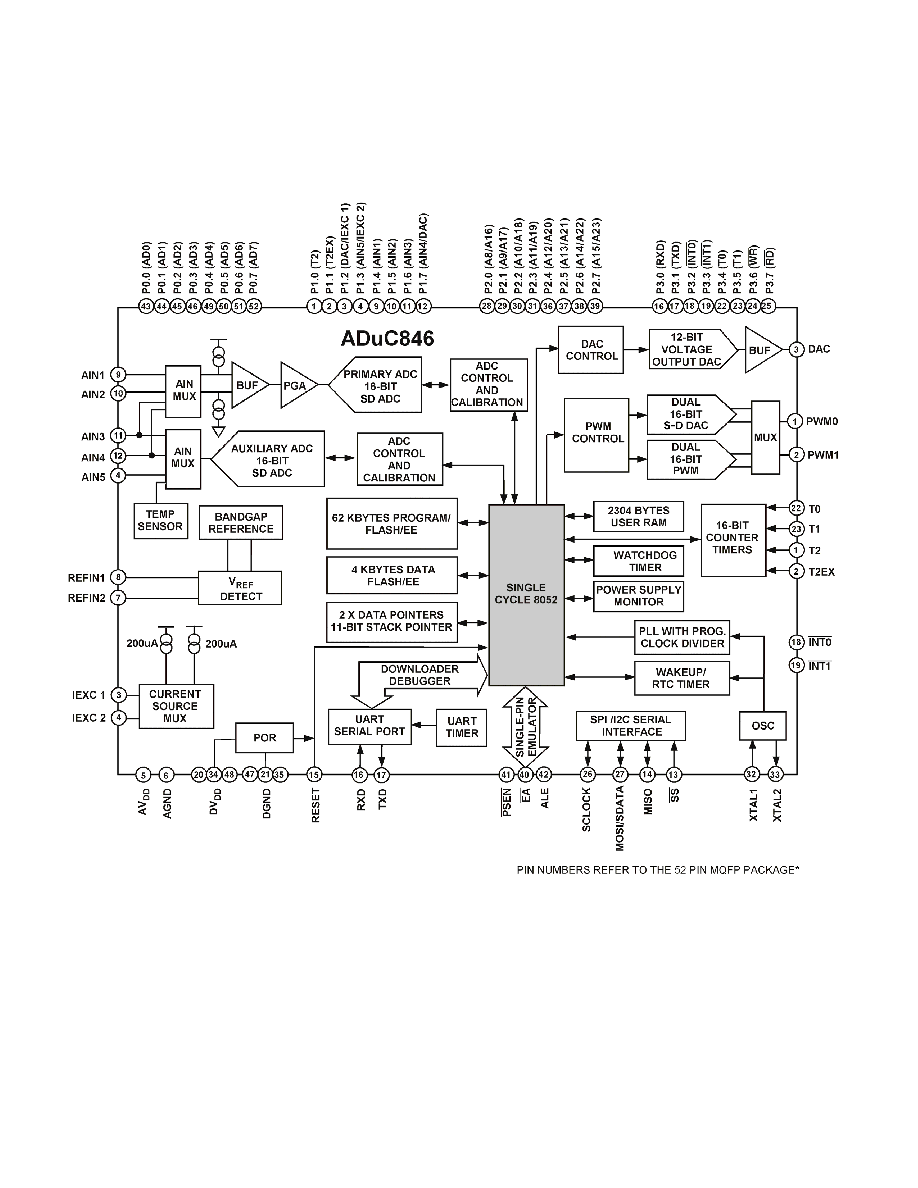
DETAILED BLOCK DIAGRAM WITH PIN NUMBERS
Figure 1: Detailed Block Diagram of the ADuC846
ADuC846
REV. PrA
-13-
PRELIMINARY TECHNICAL DATA
INTRODUCTION
The ADuC846 is a pin compatible upgrade to the ADuC836 and
provides increased core performance. The ADUC846 has a single
cycle 8052 core allowing operation at up to 12.58MIPs. It has all the
same features as the ADuC836 but the standard 12-cycle 8052 core
has been replaced with a 12.6MIPs single cycle core.
Since the ADuC846 and ADuC836 share the same feature set only
the differences between the two chips are documented here. For full
documentation on the ADuC836 please consult the datasheet
available at http://www.analog.com/microconverter
MEMORY7 ORGANISATION
The ADuC846 contains 4 different memory blocks namely:
- 62kBytes of On-Chip Flash/EE Program Memory
- 4kBytes of On-Chip Flash/EE Data Memory
- 256 Bytes of General Purpose RAM
- 2kBytes of Internal XRAM
(1) Flash/EE Program Memory
The ADuC846 provides 62kBytes of Flash/EE program memory to
run user code. The user can choose to run code from this internal
memory or run code from an external program memory.
If the user applies power or resets the device while the
EA pin is
pulled low externally, the part will execute code from the external
program space, otherwise if
EA is pulled high externally the part
defaults to code execution from its internal 62kBytes of Flash/EE
program memory. The ADuC846 does not support the rollover from
F7FFh in internal code space to F800h in external code space. Instead
the 2048 bytes between F800h and FFFFh will appear as NOP
instructions to user code.
Permanently embedded firmware allows code to be serially
downloaded to the 62kBytes of internal code space via the UART
serial port while the device is in-circuit. No external hardware is
required.
56kBytes of the program memory can be repogrammed during
runtime hence the code space can be upgraded in the field using a
user defined protocol or it can be used as a data memory. This will be
discussed in more detail in the Flash/EE Memory section of the
datasheet.
(2) Flash/EE Data Memory
4kBytes of Flash/EE Data Memory are available to the user and can
be accessed indirectly via a group of registers mapped into the
Special Function Register (SFR) area. Access to the Flash/EE Data
memory is discussed in detail later as part of the Flash/EE memory
section in this data sheet.
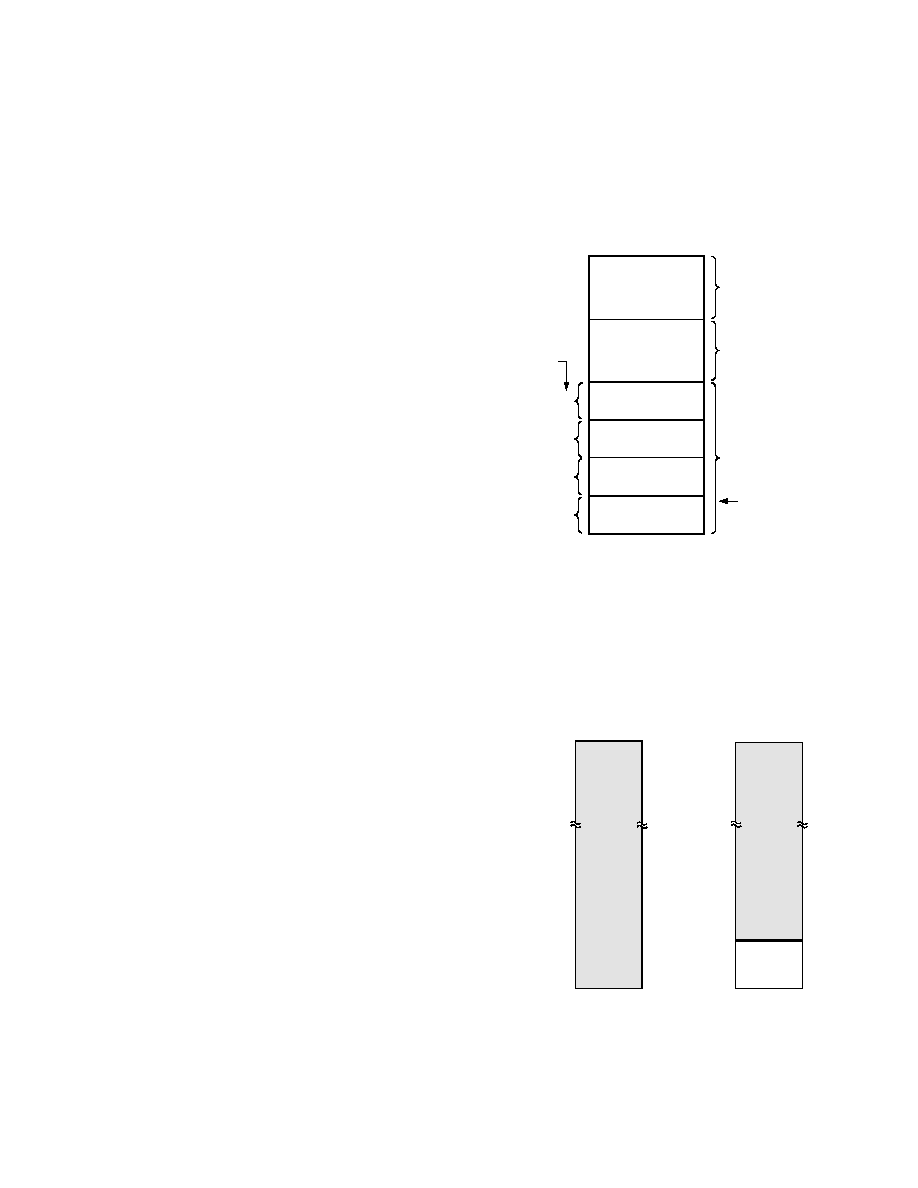
(3) General Purpose RAM
The general purpose RAM is divided into two seperate memories,
namely the upper and the lower 128 bytes of RAM. The lower 128
bytes of RAM can be accessed through direct or indirect addressing
while the upper 128 bytes of RAM can only be accessed through
indirect addressing as it shares the same address space as the SFR
space which can only be accessed through direct addressing.
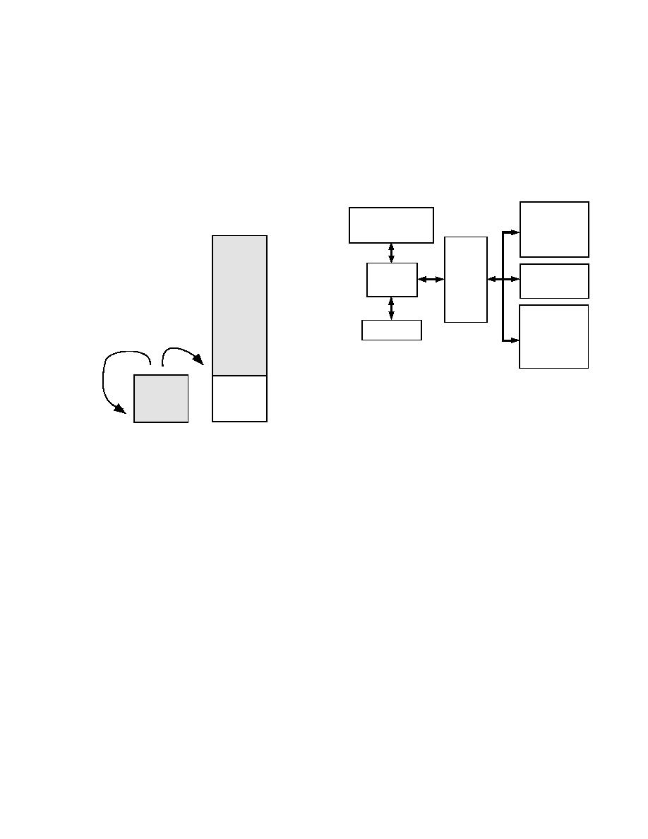
The lower 128 bytes of internal data memory are mapped as shown in
Figure 2. The lowest 32 bytes are grouped into four banks of eight
registers addressed as R0 through R7. The next 16 bytes (128 bits),
locations 20Hex through 2FHex above the register banks, form a
block of directly addressable bit locations at bit addresses 00H
through 7FH. The stack can be located anywhere in the internal
memory address space, and the stack depth can be expanded up to
2048 bytes.
Reset initializes the stack pointer to location 07 hex. Any call or push
pre-increments the SP before loading the stack. Hence loading the
stack starts from locations 08 hex which is also the first register (R0)
of register bank 1. Thus, if one is going to use more than one register
bank, the stack pointer should be initialized to an area of RAM not
used for data storage.
BIT-ADDRESSABLE
(BIT ADDRESSES)
FOUR BANKS OF EIGHT
REGISTERS
R0 R7
BANKS
SELECTED
VIA
BITS IN PSW
11
10
01
00
07H
0FH
17H
1FH
2FH
7FH
00H
08H
10H
18H
20H
RESET VALUE OF
STACK POINTER
30H
GENERAL-PURPOSE
AREA
Figure 2. Lower 128 Bytes of Internal Data Memory
(4) Internal XRAM
The ADuC846 contains 2kBytes of on-chip extended data memory.
This memory although on-chip is accessed via the MOVX
instruction. The 2kBytes of internal XRAM are mapped into the
bottom 2kBytes of the external address space if the CFG846.0 bit is
set, otherwise access to the external data memory will occur just like
a standard 8051.
Even with the CFG846.0 bit set access to the external XRAM will
occur once the 24 bit DPTR is greater than 0007FFH.
EXTERNAL
DATA
MEMORY
SPACE
(24-BIT
ADDRESS
SPACE)
000000H
FFFFFFH
CFG845.0=0
EXTERNAL
DATA
MEMORY
SPACE
(24-BIT
ADDRESS
SPACE)
000000H
FFFFFFH
CFG845.0=1
0007FFH
000800H
2 KBYTES
ON-CHIP
XRAM
Figure 3: Internal and External XRAM
When accessing the internal XRAM the P0, P2 port pins as well as
the RD and WR strobes will not be output as per a standard 8051
ADuC846
-14-
REV. PrA
PRELIMINARY TECHNICAL DATA
MOVX instruction. This allows the user to use these port pins as
standard I/O.
SPECIAL FUNCTION REGISTERS (SFRs)
The SFR space is mapped into the upper 128 bytes of internal data
memory space and accessed by direct addressing only. It provides an
interface between the CPU and all on chip peripherals. A block
diagram showing the programming model of the ADuC846 via the
SFR area is shown in Figure 5.
The upper 1792 bytes of the internal XRAM can be configured to be
used as an extended 11-bit stack pointer.
By default the stack will operate exactly like an 8052 in that it will
rollover from FFh to 00h in the general purpose RAM. On the
ADuC844 however it is possible (by setting CFG844.7) to enable the
11-bit extended stack pointer. In this case the stack will rollover from
FFh in RAM to 0100h in XRAM.
All registers except the Program Counter (PC) and the four general-
purpose register banks, reside in the SFR area. The SFR registers
include control, configuration, and data registers that provide an
interface between the CPU and all on-chip peripherals.
The 11-bit stack pointer is visable in the SP and SPH SFRs. The SP
SFR is located at 81h as with a standard 8052. The SPH SFR is
located at B7h. The 3 LSBs of this SFR contain the 3 extra bits
necessary to extend the 8-bit stack pointer into an 11-bit stack
pointer.
128-BYTE
SPECIAL
FUNCTION
REGISTER
AREA
62 KBYTE ELECTRICALLY
REPROGRAMMABLE
NONVOLATILE FLASH/EE
PROGRAM MEMORY
8051-
COMPATIBLE
CORE
OTHER ON-CHIP
PERIPHERALS
TEMP SENSOR
CURRENT SOURCES
12-BIT DAC
SERIAL I/O
WDT, PSM
TIC, PLL
DUAL
SIGMA-DELTA
ADCs
4 KBYTE
ELECTRICALLY
REPROGRAMMABLE
NONVOLATILE
FLASH/EE DATA
MEMORY
256 BYTES RAM
2K XRAM
UPPER 1792
BYTES OF
ON-CHIP XRAM
(DATA +STACK
FOR EXSP=1,
DATA ONLY
FOR EXSP=0)
256 BYTES OF
ON-CHIP DATA
RAM
(DATA + STACK)
LOWER 256
BYTES OF
ON-CHIP XRAM
(DATA ONLY)
00H
FFH
100H
00H
07FFH
CFG845.7 = 0
CFG845.7 = 1
Figure 5. Programming Model
Accumulator SFR (ACC)
ACC is the Accumulator register and is used for math operations
including addition, subtraction, integer multiplication and division,
and Boolean bit manipulations. The mnemonics for accumulator-
specific instructions refer to the Accumulator as A.
Figure 4. Extended Stack Pointer Operation
External Data Memory (External XRAM)
Just like a standard 8051 compatible core the ADuC846 can access
external data memory using a MOVX instruction. The MOVX
instruction automatically outputs the various control strobes required
to access the data memory.
B SFR (B)
The B register is used with the ACC for multiplication and division
operations. For other instructions it can be treated as a general-
purpose scratchpad register.
The ADuC846 however, can access up to 16MBytes of extrenal data
memory. This is an enhancement of the 64kBytes external data
memory space available on a standard 8051 compatible core.
Data Pointer (DPTR)
The Data Pointer is made up of three 8-bit registers, named DPP
(page byte), DPH (high byte) and DPL (low byte). These are used to
provide memory addresses for internal and external code access and
external data access. It may be manipulated as a 16-bit register
(DPTR = DPH, DPL), although INC DPTR instructions will
automatically carry over to DPP, or as three independent 8-bit
registers (DPP, DPH, DPL).
The external data memory is discussed in more detail in the
ADuC846 Hardware Design Considerations section.
The ADuC846 supports dual data pointers. Refer to the Dual Data
Pointer section later in this datasheet.
Stack Pointer (SP and SPH)
The SP SFR is the stack pointer and is used to hold an internal RAM
address that is called the `top of the stack.' The SP register is
incremented before data is stored during PUSH and CALL
executions. While the Stack may reside anywhere in on-chip RAM,
the SP register is initialized to 07H after a reset. This causes the stack
to begin at location 08H.
As mentioned earlier the ADuC846 offers an extended 11-bit stack
pointer. The 3 extra bits to make up the 11-bit stack pointer are the 3
LSBs of the SPH byte located at B7h. To enable the SPH SFR the

ADuC846
REV. PrA
-15-
PRELIMINARY TECHNICAL DATA
EXSP (CFG846.7) bit must be set otherwise the SPH SFR cannot be
read or written to.
Program Status Word (PSW)
The PSW SFR contains several bits reflecting the current status of the
CPU as detailed in Table I.
SFR Address
D0H
Power ON Default Value
00H
Bit Addressable
Yes
Table I. PSW SFR Bit Designations
Bit Name
Description
7 CY
Carry
Flag
6
AC
Auxiliary Carry Flag
5 F0
General-Purpose
Flag
4
RS1
Register Bank Select Bits
3 RS0
RS1 RS0 Selected
Bank
0 0 0
0 1 1
1 0 2
1 1 3
2 OV
Overflow
Flag
1 F1
General-Purpose
Flag
0 P
Parity
Bit
The PCON SFR contains bits for power-saving options and general-
purpose status flags as shown in Table II.
SFR Address
87H
Power ON Default Value
00H
Bit Addressable
No
Table II. PCON SFR Bit Designations
Bit Name
Description
7
SMOD
Double UART Baud Rate
6
SERIPD SPI Power-Down Interrupt Enable
5
INT0PD INT0 Power-Down Interrupt Enable
4
ALEOFF Disable ALE Output
3
GF1
General-Purpose Flag Bit
2
GF0
General-Purpose Flag Bit
1
PD
Power-Down Mode Enable
0
IDL
Idle Mode Enable
The CFG846 SFR contains the necessary bits to configure the
internal XRAM and the extended SP. By default it configures the
user into 8051 mode. i.e. extended SP is disabled, internal XRAM is
disabled.
SFR Address
AFhH
Power ON Default Value
00H
Bit Addressable
No
Table III. CFG846 SFR Bit Designations
Bit Name
Description
7
EXSP
Extended SP Enable
If this bit is set then the stack will
rollover from SPH/SP = 00FFh to
0100h.
If this bit is clear then the SPH SFR will be
disabled and the stack will rollover from SP=FFh to
SP = 00h
6
----
----
5
----
----
4
----
----
3
----
----
2
----
----
1
----
----
0
XRAMEN XRAM Enable Bit
If this bit is set then the internal
XRAM will be mapped into the lower
2kBytes of the external address space.
If this bit is clear then the internal
XRAM will not be accessible and the
external data memory will be mapped
into the lower 2kBytes of external data
memory. (see figure 3)
ADuC846
-16-
REV. PrA
PRELIMINARY TECHNICAL DATA
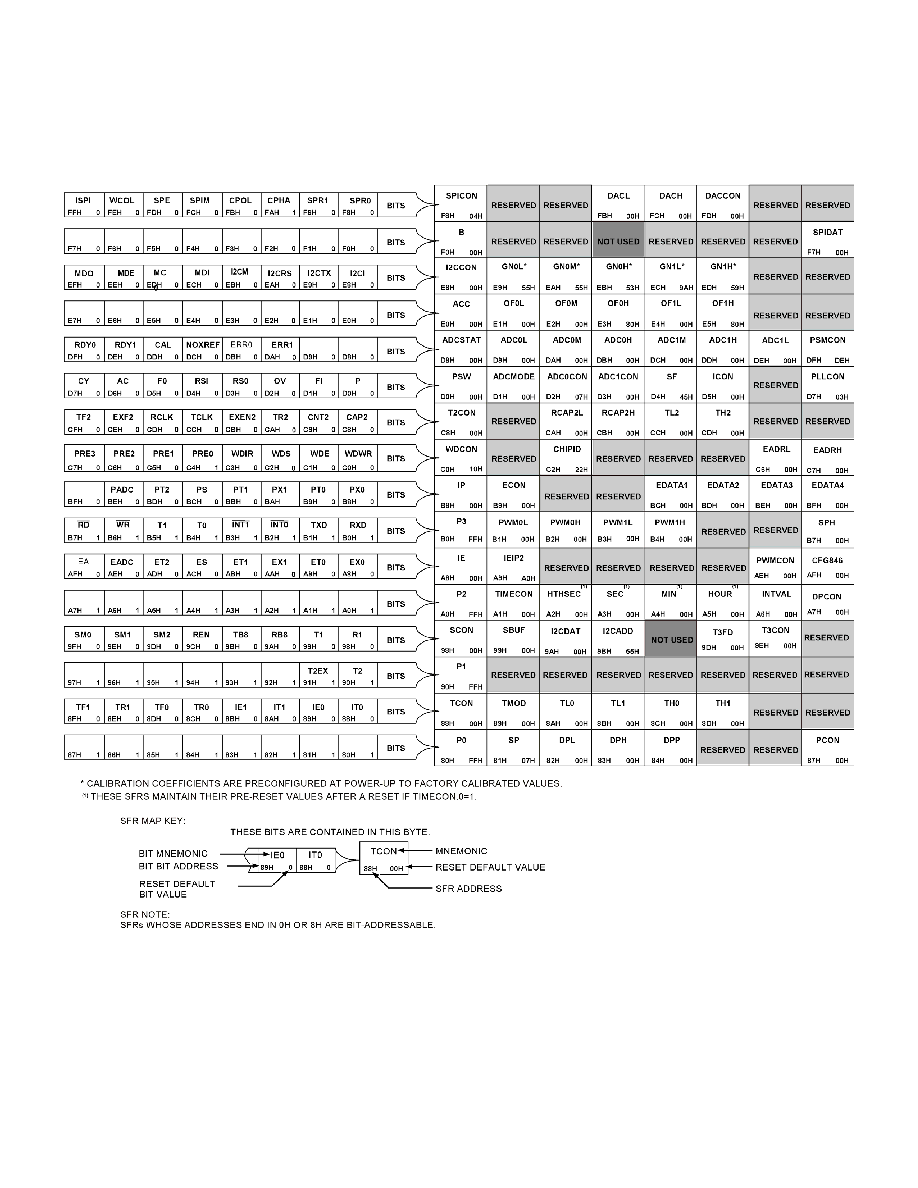
COMPLETE SFR MAP
Figure 6 below shows a full SFR memory map and the SFR contents after RESET. NOT USED indicates unoccupied SFR locations. Unoccupied locations
in the SFR address space are not implemented; i.e., no register exists at this location. If an unoccupied location is read, an unspecified value is
returned. SFR locations that are reserved for future use are shaded (RESERVED) and should not be accessed by user software.
Figure 6: Complete SFR Map
ADuC846
REV. PrA
-17-
PRELIMINARY TECHNICAL DATA
8052 Instruction Set
The following pages document the number of clock cycles required
for each instruction. Most instructions are executed in one or two
clock cycles resulting in 12.6MIPs peak performance when
operating at PLLCON = 00H.
Timer Operation
Timers on a standard 8052 increment by one with each machine
cycle. On the ADuC846 one machine cycle is equal to one clock
cycle hence the timers will increment at the same rate as the core
clock.
ALE
The output on the ALE pin on the ADuC836 was a clock at 1/6th of
the core operating frequency. On the ADuC846 the ALE pin
operates as follows.
For a single machine cycle instruction: ALE is high for the first
half of the machine cycle and low for the second half. The ALE
output is at the core operating frequency.For a two or more
machine cycle instruction: ALE is high for the first half of the first
machine cycle and then low for the rest of the machine cycles.
External Memory Access
There is no support for external program memory access on the
ADuC846. When accessing external RAM the EWAIT register
may need to be programmed in order to give extra machine cycles
to MOVX commands. This is to account for differing external
RAM access speeds.
INSTRUCTION TABLE
TABLE IV: Optimized Single Cycle 8051 Instruction Set
Mnemonic Arithmetic
Description
Bytes
Cycles
ARITHMETIC
ADD A,Rn
Add register to A
1
1
ADD A,@Ri
Add indirect memory to A
1
2
ADDC A,Rn
Add register to A with carry
1
1
ADDC A,@Ri
Add indirect memory to A with carry
1
2
ADD A,dir
Add direct byte to A
2
2
ADD A,#data
Add direct byte to A with carry
2
2
SUBB A,Rn
Subtract register from A with borrow
1
1
SUBB A,@Ri
Subtract indirect memory from A with borrow
1
2
SUBB A,dir
Subtract direct from A with borrow
2
2
SUBB A,#data
Subtract immediate from A with borrow
1
1
INC A
Increment A
1
1
INC Rn
Increment register
1
1
INC @Ri
Increment indirect memory
1
2
INC dir
Increment direct byte
2
2
INC DPTR
Increment data pointer
1
3
DEC A
Decrement A
1
1
DEC Rn
Decrement Register
1
1
DEC @Ri
Decrement indirect memory
1
2
DEC dir
Decrement direct byte
2
2
MUL AB
Multiply A by B
1
9
DIV AB
Divide A by B
1
9
DA A
Decimal Adjust A
1
2
ADuC846
PRELIMINARY TECHNICAL DATA
Mnemonic Arithmetic
Description
Bytes
Cycles
LOGIC
ANL A,Rn
AND register to A
1
1
ANL A,@Ri
AND indirect memory to A
1
2
ANL A,dir
AND direct byte to A
2
2
ANL A,#data
AND immediate to A
2
2
ANL dir,A
AND A to direct byte
2
2
ANL dir,#data
AND immediate data to direct byte
3
3
ORL A,Rn
OR register to A
1
1
ORL A,@Ri
OR indirect memory to A
1
2
ORL A,dir
OR direct byte to A
2
2
ORL A,#data
OR immediate to A
2
2
ORL dir,A
OR A to direct byte
2
2
ORL dir,#data
OR immediate data to direct byte
3
3
XRL A,Rn
Exclusive-OR register to A
1
1
XRL A,@Ri
Exclusive-OR indirect memory to A
2
2
XRL A,#data
Exclusive-OR immediate to A
2
2
XRL dir,A
Exclusive-OR A to direct byte
2
2
XRL A,dir
Exclusive-OR indirect memory to A
2
2
XRL dir,#data
Exclusive-OR immediate data to direct
3
3
CLR A
Clear A
1
1
CPL A
Complement A
1
1
SWAP A
Swap Nibbles of A
1
1
RL A
Rotate A left
1
1
RLC A
Rotate A left through carry
1
1
RR A
Rotate A right
1
1
RRC A
Rotate A right through carry
1
1
BOOLEAN
CLR C
Clear carry
1
1
CLR bit
Clear direct bit
2
2
SETB C
Set Carry
1
1
SETB bit
Set direct bit
2
2
CPL C
Complement carry
1
1
CPL bit
Complement direct bit
2
2
ANL C,bit
AND direct bit and carry
2
2
ANL C,/bit
AND direct bit inverse to carry
2
2
ORL C,bit
OR direct bit and carry
2
2
ORL C,/bit
OR direct bit inverse to carry
2
2
MOV C,bit
Move direct bit to carry
2
2
MOV bit,C
Move carry to direct bit
2
2
-18-
REV. PrA
ADuC846
PRELIMINARY TECHNICAL DATA
Mnemonic Arithmetic
Description
Bytes
Cycles
BRANCHING
JMP @A+DPTR
Jump indirect relative to DPTR
1
3
RET
Return from subroutine
1
4
RETI
Return from interrupt
1
4
ACALL addr11
Absolute jump to subroutine
2
3
AJMP addr11
Absolute jump unconditional
2
3
SJMP rel
Short jump (relative address)
2
3
JC rel
Jump on carry = 1
2
3
JNC rel
Jump on carry = 0
2
3
JZ rel
Jump on accumulator = 0
2
3
JNZ rel
Jump on accumulator != 0
2
3
DJNZ Rn,rel
Decrement register, jnz relative
2
3
LJMP
Long jump unconditional
3
4
LCALL addr16
Long jump to subroutine
3
4
JB bit,rel
Jump on direct bit = 1
3
4
JNB bit,rel
Jump on direct bit = 0
3
4
JBC bit,rel
Jump on direct bit = 1 and clear
3
4
CJNE A,dir,rel
Compare A, direct JNE relative
3
4
CJNE A,#data,rel
Compare A, immediate JNE relative
3
4
CJNE Rn,#data,rel
Compare register, immediate JNE relative
3
4
CJNE @Ri,#data,rel
Compare indirect, immediate JNE relative
3
4
DJNZ dir,rel
Decrement direct byte, JNZ relative
3
4
MISCELLANEOUS
NOP
No operation
1
1
Notes:
1. One cycle is one clock.
2. Cycles of MOVX instructions are 4 cycles when they have 0 wait state. Cycles of MOVX instructions are 4+N cycles when they have N wait
states.
3. Cycles of LCALL instruction are 3 cycles when the LCALL instruction comes from interrupt.
REV. PrA
-19-
ADuC846
-20-
REV. PrA
PRELIMINARY TECHNICAL DATA
Document Outline