Äîêóìåíòàöèÿ è îïèñàíèÿ www.docs.chipfind.ru
Differential Input, 1 MSPS
10-Bit and 12-Bit ADCs in an 8-Lead SOT-23
AD7440/AD7450A
Rev. B
Information furnished by Analog Devices is believed to be accurate and reliable.
However, no responsibility is assumed by Analog Devices for its use, nor for any
infringements of patents or other rights of third parties that may result from its use.
Specifications subject to change without notice. No license is granted by implication
or otherwise under any patent or patent rights of Analog Devices. Trademarks and
registered trademarks are the property of their respective owners.
One Technology Way, P.O. Box 9106, Norwood, MA 02062-9106, U.S.A.
Tel: 781.329.4700
www.analog.com
Fax: 781.326.8703
© 2004 Analog Devices, Inc. All rights reserved.
FEATURES
Fast throughput rate: 1 MSPS
Specified for V
DD
of 3 V and 5 V
Low power at max throughput rate:
4 mW max at 1 MSPS with 3 V supplies
9.25 mW max at 1 MSPS with 5 V supplies
Fully differential analog input
Wide input bandwidth:
70 dB SINAD at 100 kHz input frequency
Flexible power/serial clock speed management
No pipeline delays
High speed serial interface:
SPI®/QSPITM/MICROWIRETM/DSP
compatible
Power-down mode: 1 µA max
8-lead SOT-23 and MSOP packages
APPLICATIONS
Transducer interface
Battery-powered systems
Data acquisition systems
Portable instrumentation
Motor control
GENERAL DESCRIPTION
The AD7440/AD7450A
1
are 10-bit and 12-bit high speed, low
power, successive approximation (SAR) analog-to-digital
converters with a fully differential analog input. These parts
operate from a single 3 V or 5 V power supply and use advanced
design techniques to achieve very low power dissipation at
throughput rates up to 1 MSPS. The SAR architecture of these
parts ensures that there are no pipeline delays.
The parts contain a low noise, wide bandwidth, differential
track-and-hold amplifier (T/H) that can handle input
frequencies up to 3.5 MHz. The reference voltage is applied
externally to the V
REF
pin and can be varied from 100 mV to
3.5 V depending on the power supply and what suits the
application. The value of the reference voltage determines the
common-mode voltage range of the part. With this truly
differential input structure and variable reference input, the user
can select a variety of input ranges and bias points.
The conversion process and data acquisition are controlled
using CS and the serial clock, allowing the device to interface
with microprocessors or DSPs. The input signals are sampled
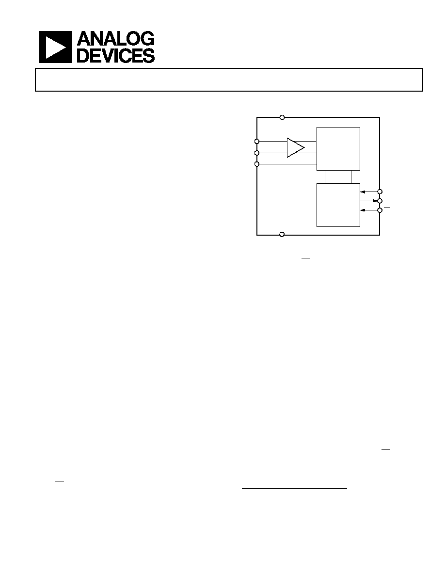
FUNCTIONAL BLOCK DIAGRAM
03051-A
-
001
V
REF
T/H
CONTROL LOGIC
12-BIT
SUCCESSIVE
APPROXIMATION
ADC
GND
SCLK
SDATA
CS
V
DD
AD7440/AD7450A
V
IN+
V
IN
Figure 1.
on the falling edge of CS; the conversion is also initiated at this
point. The SAR architecture of these parts ensures that there are
no pipeline delays. The AD7440 and the AD7450A use ad-
vanced design techniques to achieve very low power dissipation
at high throughput rates.
PRODUCT HIGHLIGHTS
1.
Operation with either 3 V or 5 V power supplies.
2.
High throughput with low power consumption.
With a 3 V supply, the AD7440/AD7450A offer 4 mW
max power consumption for 1 MSPS throughput.
3.
Fully differential analog input.
4.
Flexible power/serial clock speed management.
The conversion rate is determined by the serial clock,
allowing the power to be reduced as the conversion time
is reduced through the serial clock speed increase. These
parts also feature a shutdown mode to maximize power
efficiency at lower throughput rates.
5.
Variable voltage reference input.
6.
No pipeline delay.
7.
Accurate control of the sampling instant via a CS input and
once-off conversion control.
8.
ENOB > eight bits typically with 100 mV reference.
1
Protected by U.S. Patent Number 6,681,332.

AD7440/AD7450A
Rev. B | Page 2 of 28
TABLE OF CONTENTS
AD7440Specifications.................................................................... 3
AD7450ASpecifications................................................................. 5
Timing Specifications....................................................................... 7
Absolute Maximum Ratings............................................................ 8
ESD Caution.................................................................................. 8
Pin Configurations and Function Descriptions ........................... 9
Terminology .................................................................................... 10
AD7440/AD7450ATypical Performance Characteristics ....... 12
Circuit Information ........................................................................ 15
Converter Operation.................................................................. 15
ADC Transfer Function............................................................. 15
Typical Connection Diagram ................................................... 16
Analog Input ............................................................................... 16
Driving Differential Inputs........................................................ 18
Digital Inputs .............................................................................. 20
Reference ..................................................................................... 20
Single-Ended Operation............................................................ 20
Serial Interface ............................................................................ 21
Modes of Operation ....................................................................... 23
Normal Mode.............................................................................. 23
Power-Down Mode .................................................................... 23
Power-Up Time .......................................................................... 24
Power vs. Throughput Rate....................................................... 24
Microprocessor and DSP Interfacing ...................................... 25
Grounding and Layout Hints.................................................... 26
Evaluating the AD7440/AD7450A Performance ................... 26
Outline Dimensions ....................................................................... 27
Ordering Guide............................................................................... 28
REVISION HISTORY
2/04--Data Sheet changed from Rev. A to Rev. B
Added Patent Note .............................................................................. 1
1/04--Data Sheet changed from Rev. 0 to Rev. A
Updated Format.................................................................... Universal
Changes to General Description ....................................................... 1
Changes to Table 1 footnotes ............................................................. 3
Changes to Table 2 footnotes ............................................................. 5
Changes to Table 3 footnotes ............................................................. 7
AD7440/AD7450A
Rev. B | Page 3 of 28
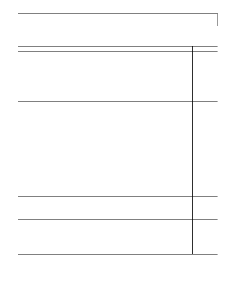
AD7440SPECIFICATIONS
Table 1. V
DD
= 2.7 V to 3.6 V, f
SCLK
= 18 MHz, f
S
= 1 MSPS, V
REF
= 2.0 V; V
DD
= 4.75 V to 5.25 V, f
SCLK
= 18 MHz, f
S
= 1 MSPS,
V
REF
= 2.5 V; V
CM
1
= V
REF
; T
A
= T
MIN
to T
MAX
, unless otherwise noted. Temperature range for B Version 40°C to +85°C.
Parameter
Test Conditions/Comments
B Version
Unit
DYNAMIC PERFORMANCE
f
IN
= 100 kHz
Signal-to-(Noise + Distortion) (SINAD)
2
61
dB min
Total Harmonic Distortion (THD)
2
82 dB typ
74
dB max
Peak Harmonic or Spurious Noise
2
82 dB typ
76
dB max
Intermodulation Distortion (IMD)
2
fa = 90 kHz, fb = 110 kHz
Second-Order Terms
83
dB typ
Third-Order Terms
83
dB typ
Aperture Delay
2
5
ns typ
Aperture Jitter
2
50
ps typ
Full Power Bandwidth
2,
3
@ 3 dB
20
MHz typ
@ 0.1 dB
2.5
MHz typ
DC ACCURACY
Resolution
10
Bits
Integral Nonlinearity (INL)
2
±0.5
LSB max
Differential Nonlinearity (DNL)
2
Guaranteed no missed codes to 10 bits
±0.5
LSB max
Zero-Code Error
2
±2.5
LSB max
Positive Gain Error
2
±1
LSB max
Negative Gain Error
2
±1
LSB max
ANALOG INPUT
Full-Scale Input Span
2 × V
REF
4
V
IN+
V
IN
V
Absolute Input Voltage
V
IN+
V
CM
= V
REF
V
CM
± V
REF
/2
V
V
IN
V
CM
= V
REF
V
CM
± V
REF
/2
V
DC Leakage Current
±1
µA max
Input Capacitance
When in track-and-hold
30/10
pF typ
REFERENCE INPUT
V
REF
Input Voltage
V
DD
= 4.75 V to 5.25 V (±1% tolerance for
specified performance)
2.5
5
V
V
DD
= 2.7 V to 3.6 V (±1% tolerance for specified
performance)
2.0
6
V
DC Leakage Current
± 1
µA max
V
REF
Input Capacitance
When in track-and-hold
10/30
pF typ
LOGIC INPUTS
Input High Voltage, V
INH
2.4
V min
Input Low Voltage, V
INL
0.8
V max
Input Current, I
IN
Typically 10 nA, V
IN
= 0 V or V
DD
±1
µA max
Input Capacitance, C
IN
7
10
pF max
LOGIC OUTPUTS
Output High Voltage, V
OH
V
DD
= 4.75 V to 5.25 V; I
SOURCE
= 200 µA
2.8
V min
V
DD
= 2.7 V to 3.6 V; I
SOURCE
= 200 µA
2.4
V min
Output Low Voltage, V
OL
I
SINK
= 200 µA
0.4
V max
Floating-State Leakage Current
±1
µA max
Floating-State Output Capacitance
7
10
pF
max
Output Coding
Twos Complement
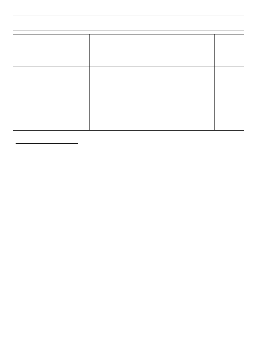
AD7440/AD7450A
Rev. B | Page 4 of 28
Parameter
Test Conditions/Comments
B Version
Unit
CONVERSION RATE
Conversion Time
888 ns with an 18 MHz SCLK
16
SCLK cycles
Track-and-Hold Acquisition Time
2
Sine wave input
200
ns max
Step input
290
ns max
Throughput Rate
1
MSPS max
POWER REQUIREMENTS
V
DD
Range: 3 V + 20%/10%; 5 V ± 5%
2.7/5.25
V min/V max
I
DD
8
Normal Mode (Static)
SCLK on or off
0.5
mA typ
Normal Mode (Operational)
V
DD
= 4.75 V to 5.25 V
1.95
mA max
V
DD
= 2.7 V to 3.6 V
1.45
mA max
Full Power-Down Mode
SCLK on or off
1
µA max
Power Dissipation
Normal Mode (Operational)
V
DD
= 5 V, 1.55 mW typ for 100 kSPS
9
9.25
mW max
V
DD
= 3 V, 0.6 mW typ for 100 kSPS
9
4
mW max
Full Power-Down
V
DD
= 5 V, SCLK on or off
5
µW max
V
DD
= 3 V, SCLK on or off
3
µW max
1
Common-mode voltage. The input signal can be centered on a dc common-mode voltage in the range specified in Figure 28 and Figure 29.
2
See Terminology section.
3
Analog inputs with slew rates exceeding 27 V/µs (full-scale input sine wave > 3.5 MHz) within the acquisition time may cause the converter to return an
incorrect result.
4
Because the input spans of V
IN+
and V
IN
are both V
REF
and are 180°out of phase, the differential voltage is 2 × V
REF
.
5
The AD7440 is functional with a reference input from 100 mV and for V
DD
= 5 V; the reference can range up to 3.5 V.
6
The AD7440 is functional with a reference input from 100 mV and for V
DD
= 3 V; the reference can range up to 2.2 V.
7
Guaranteed by characterization.
8
Measured with a midscale dc input.
9
See Power vs. Throughput section.
AD7440/AD7450A
Rev. B | Page 5 of 28
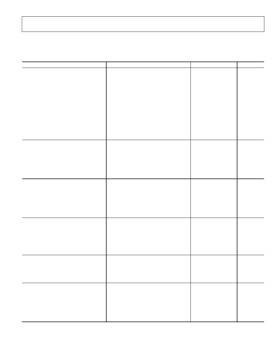
AD7450ASPECIFICATIONS
Table 2. V
DD
= 2.7 V to 3.6 V, f
SCLK
= 18 MHz, f
S
= 1 MSPS, V
REF
= 2.0 V; V
DD
= 4.75 V to 5.25 V, f
SCLK
= 18 MHz, f
S
= 1 MSPS,
V
REF
= 2.5 V; V
CM
1
= V
REF
; T
A
= T
MIN
to T
MAX
, unless otherwise noted. Temperature range for B Version 40°C to +85°C.
Parameter
Test Conditions/Comments
B Version
Unit
DYNAMIC PERFORMANCE
f
IN
= 100 kHz
Signal-to-(Noise + Distortion) (SINAD)
2
70
dB min
Total Harmonic Distortion (THD)
2
V
DD
= 4.75 V to 5.25 V, 86 dB typ
76
dB max
V
DD
= 2.7 V to 3.6 V, 84 dB typ
74
dB max
Peak Harmonic or Spurious Noise
2
V
DD
= 4.75 V to 5.25 V, 86 dB typ
76
dB max
V
DD
= 2.7 V to 3.6 V, 84 dB typ
74
dB max
Intermodulation Distortion (IMD)
2
fa = 90 kHz, fb = 110 kHz
Second-Order Terms
89
dB typ
Third-Order Terms
89
dB typ
Aperture Delay
2
5
ns typ
Aperture Jitter
2
50
ps typ
Full Power Bandwidth
2, 3
@ 3 dB
20
MHz typ
@ 0.1 dB
2.5
MHz typ
DC ACCURACY
Resolution
12
Bits
Integral Nonlinearity (INL)
2
±1
LSB max
Differential Nonlinearity (DNL)
2
Guaranteed no missed codes to 12 bits
±0.95
LSB max
Zero-Code Error
2
±6
LSB max
Positive Gain Error
2
±2
LSB max
Negative Gain Error
2
±2
LSB max
ANALOG INPUT
Full-Scale Input Span
2 × V
REF
4
V
IN+
V
IN
V
Absolute Input Voltage
V
IN+
V
CM
= V
REF
V
CM
± V
REF
/2
V
V
IN
V
CM
= V
REF
V
CM
± V
REF
/2
V
DC Leakage Current
±1
µA max
Input Capacitance
When in track-and-hold
30/10
pF typ
REFERENCE INPUT
V
REF
Input Voltage
V
DD
= 4.75 V to 5.25 V
(±1% tolerance for specified performance)
2.5
5
V
V
DD
= 2.7 V to 3.6 V
(±1% tolerance for specified performance)
2.0
6
V
DC Leakage Current
±1
µA max
V
REF
Input Capacitance
When in track-and-hold
10/30
pF typ
LOGIC INPUTS
Input High Voltage, V
INH
2.4
V min
Input Low Voltage, V
INL
0.8
V max
Input Current, I
IN
Typically 10 nA, V
IN
= 0 V or V
DD
±1
µA max
Input Capacitance, C
IN
7
10
pF max
LOGIC OUTPUTS
Output High Voltage, V
OH
V
DD
= 4.75 V to 5.25 V; I
SOURCE
= 200 µA
2.8
V min
V
DD
= 2.7 V to 3.6 V; I
SOURCE
= 200 µA
2.4
V min
Output Low Voltage, V
OL
I
SINK
= 200 µA
0.4
V max
Floating-State Leakage Current
±1
µA max
Floating-State Output Capacitance
7
10
pF max
Output Coding
Twos Complement
AD7440/AD7450A
Rev. B | Page 6 of 28
Parameter
Test Conditions/Comments
B Version
Unit
CONVERSION RATE
Conversion Time
888 ns with an 18 MHz SCLK
16
SCLK cycles
Track-and-Hold Acquisition Time
2
Sine wave input
200
ns max
Step input
290
ns max
Throughput Rate
1
MSPS max
POWER REQUIREMENTS
V
DD
Range: 3 V + 20%/10%; 5 V ± 5%
2.7/5.25
V min/V max
I
DD
8
Normal Mode (Static)
SCLK on or off
0.5
mA typ
Normal Mode (Operational)
V
DD
= 4.75 V to 5.25 V
1.95
mA max
V
DD
= 2.7 V to 3.6 V
1.45
mA max
Full Power-Down Mode
SCLK on or off
1
µA max
Power Dissipation
Normal Mode (Operational)
V
DD
= 5 V, 1.55 mW typ for 100 kSPS
9
9.25
mW max
V
DD
= 3 V, 0.6 mW typ for 100 kSPS
9
4
mW max
Full Power-Down
V
DD
= 5 V, SCLK on or off
5
µW max
V
DD
= 3 V, SCLK on or off
3
µW max
1
Common-mode voltage. The input signal can be centered on a dc common-mode voltage in the range specified in Figure 28 and Figure 29.
2
See Terminology section.
3
Analog inputs with slew rates exceeding 27 V/µs (full-scale input sine wave > 3.5 MHz) within the acquisition time may cause the converter to return an
incorrect result.
4
Because the input spans of V
IN+
and V
IN
are both V
REF
and are 180° out of phase, the differential voltage is 2 × V
REF
.
5
The AD7450A is functional with a reference input from 100 mV and for V
DD
= 5 V; the reference can range up to 3.5 V.
6
The AD7450A is functional with a reference input from 100 mV and for V
DD
= 3 V; the reference can range up to 2.2 V.
7
Guaranteed by characterization.
8
Measured with a midscale dc input.
9
See Power vs. Throughput section.
AD7440/AD7450A
Rev. B | Page 7 of 28
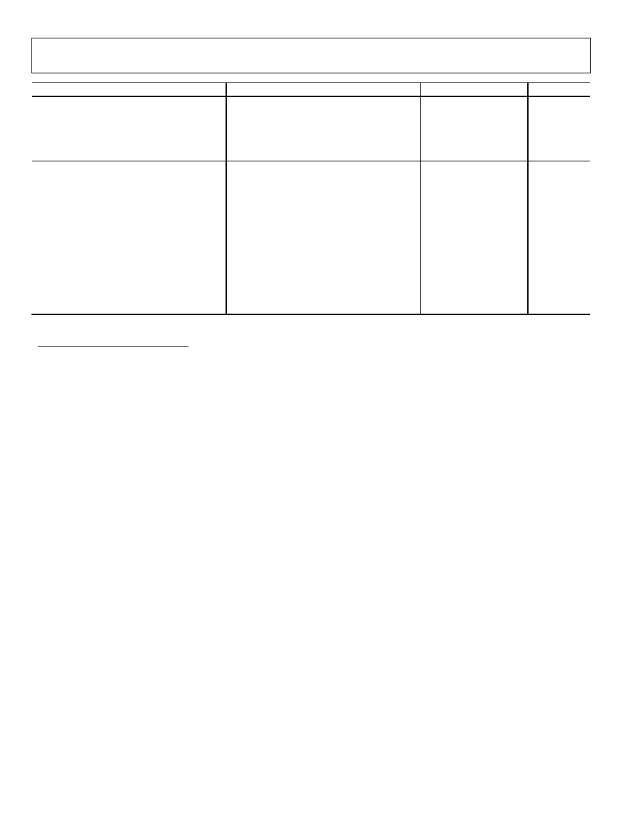
TIMING SPECIFICATIONS
Guaranteed by characterization. All input signals are specified with tr = tf = 5 ns (10% to 90% of V
DD
) and timed from a voltage level of
1.6 V. See Figure 2, Figure 3, and the Serial Interface section.
Table 3. V
DD
= 2.7 V to 3.6 V, f
SCLK
= 18 MHz, f
S
= 1 MSPS, V
REF
= 2.0 V; V
DD
= 4.75 V to 5.25 V, f
SCLK
= 18 MHz, f
S
= 1 MSPS,
V
REF
= 2.5 V; V
CM
1
= V
REF
; T
A
= T
MIN
to T
MAX
, unless otherwise noted.
Parameter
Limit at T
MIN
, T
MAX
Unit
Description
f
SCLK
2
10
kHz min
18
MHz max
t
CONVERT
16 × t
SCLK
t
SCLK
= 1/f
SCLK
888
ns max
t
QUIET
60
ns min
Minimum quiet time between the end of a serial read and the next falling edge of CS
t
1
10
ns min
Minimum CS pulse width
t
2
10
ns min
CS falling edge to SCLK falling edge setup time
t
3
3
20
ns max
Delay from CS falling edge until SDATA three-state disabled
t
4
3
40
ns max
Data access time after SCLK falling edge
t
5
0.4 t
SCLK
ns min
SCLK high pulse width
t
6
0.4 t
SCLK
ns min
SCLK low pulse width
t
7
10
ns min
SCLK edge to data valid hold time
t
8
4
10
ns min
SCLK falling edge to SDATA three-state enabled
35
ns max
SCLK falling edge to SDATA three-state enabled
t
POWER-UP
5
1
µs max
Power-up time from full power-down
1
Common-mode voltage.
2
Mark/space ratio for the SCLK input is 40/60 to 60/40.
3
Measured with the load circuit of
and defined as the time required for the output to cross 0.8 V or 2.4 V with V
Figure 4
Figure 4.
DD
= 5 V or 0.4 V or 2.0 V for V
DD
= 3 V.
4
t
8
is derived from the measured time taken by the data outputs to change 0.5 V when loaded with the circuit of
The measured number is then extrapolated
back to remove the effects of charging or discharging the 25 pF capacitor. This means that the time, t
8
, quoted in the Timing Specifications is the true bus relinquish
time of the part and is independent of the bus loading.
5
See Power-Up Time section.
t
3
t
2
t
4
t
7
t
8
t
6
t
1
t
5
t
QUIET
t
CONVERT
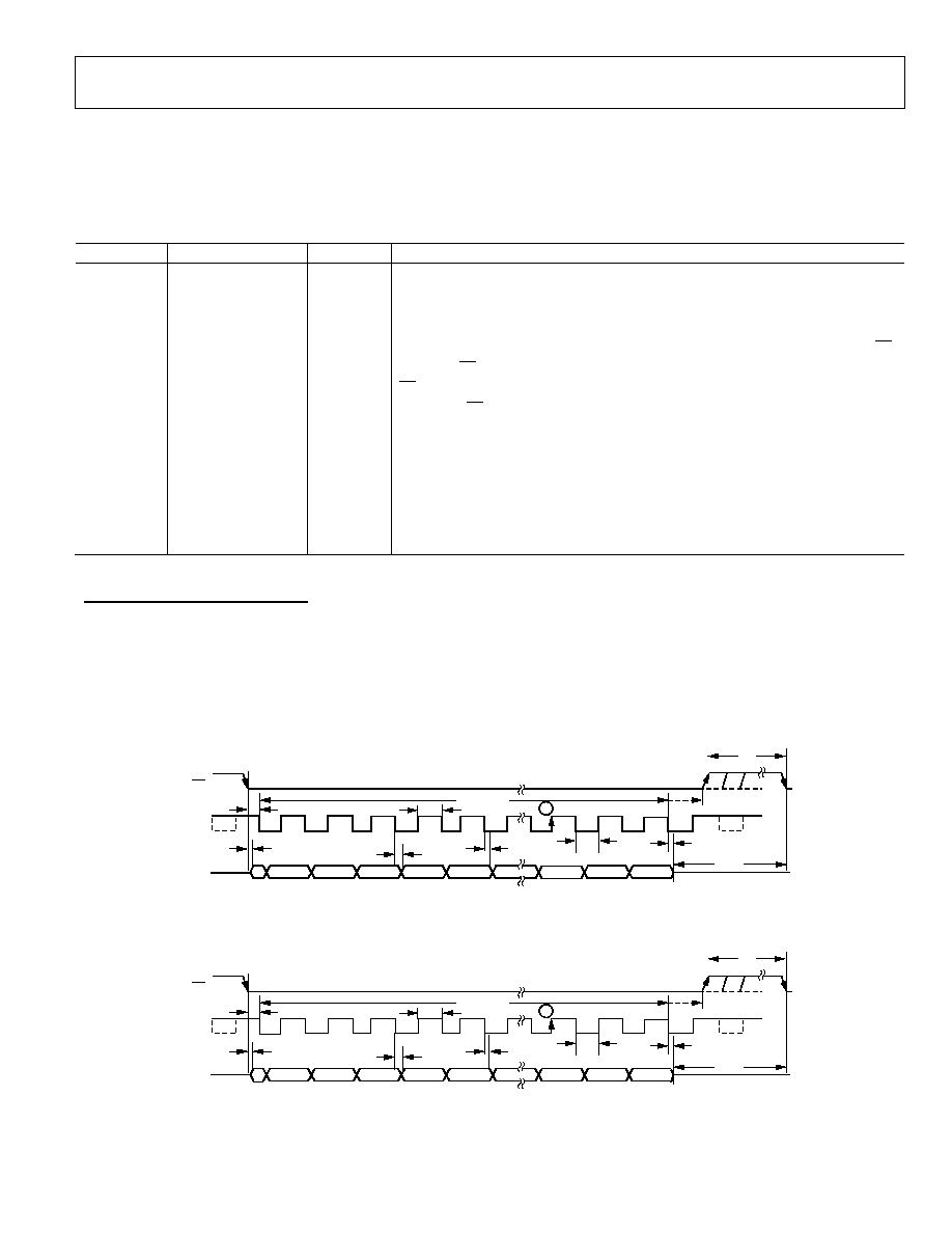
CS
SCLK
SDATA
4 LEADING ZEROS
THREE-STATE
1
2
3
4
5
13
14
15
16
0
0
0
0
DB11
DB10
DB2
DB1
DB0
B
03051-A
-
002
Figure 2. AD7450A Serial Interface Timing Diagram
t
3
t
2
t
4
t
7
t
8
t
6
t
1
t
5
t
QUIET
t
CONVERT
CS
SCLK
SDATA
4 LEADING ZEROS
2 TRAILING ZEROS THREE-STATE
1
2
3
4
5
13
14
15
16
0
0
0
0
DB9
DB8
DB0
0
0
B
03051-A
-
003
Figure 3. AD7440 Serial Interface Timing Diagram
AD7440/AD7450A
Rev. B | Page 8 of 28
ABSOLUTE MAXIMUM RATINGS
T
A
= 25°C, unless otherwise noted.
Table 4.
Parameter Rating
V
DD
to GND
0.3 V to +7 V
V
IN+
to GND
0.3 V to V
DD
+ 0.3 V
V
IN
to GND
0.3 V to V
DD
+ 0.3 V
Digital Input Voltage to GND
0.3 V to +7 V
Digital Output Voltage to GND
0.3 V to V
DD
+ 0.3 V
V
REF
to GND
0.3 V to V
DD
+ 0.3 V
Input Current to Any Pin Except Supplies
1
±10 mA
Operating Temperature Range
Commercial (B Version)
40°C to +85°C
Storage Temperature Range
65°C to +150°C
Junction Temperature
150°C
JA
Thermal Impedance
MSOP 205.9°C/W
SOT-23 211.5°C/W
JC
Thermal Impedance
MSOP 43.74°C/W
SOT-23 91.99°C/W
Lead Temperature, Soldering
Vapor Phase (60 secs)
215°C
Infrared (15 secs)
220°C
ESD 1
kV
Stresses above those listed under Absolute Maximum Ratings
may cause permanent damage to the device. This is a stress
rating only; functional operation of the device at these or any
other conditions above those listed in the operational sections
of this specification is not implied. Exposure to absolute
maximum rating conditions for extended periods may affect
device reliability.
1
Transient currents of up to 100 mA do not cause SCR latch up.
03051-A
-
004
1.6mA
I
OL
200
µ
A
I
OH
1.6V
TO OUTPUT
PIN
C
L
25pF
Figure 4. Load Circuit for Digital Output Timing Specifications
ESD CAUTION
ESD (electrostatic discharge) sensitive device. Electrostatic charges as high as 4000 V readily accumulate on the
human body and test equipment and can discharge without detection. Although this product features
proprietary ESD protection circuitry, permanent damage may occur on devices subjected to high energy
electrostatic discharges. Therefore, proper ESD precautions are recommended to avoid performance
degradation or loss of functionality.
AD7440/AD7450A
Rev. B | Page 9 of 28
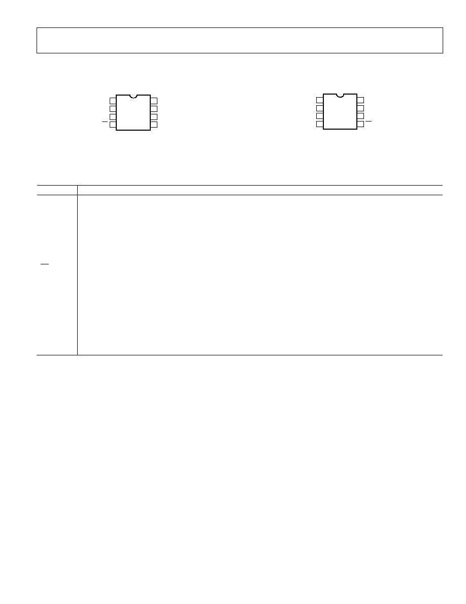
PIN CONFIGURATIONS AND FUNCTION DESCRIPTIONS
03051-A
-
005
V
REF
V
IN+
V
IN
GND
8
7
6
5
V
DD
1
SCLK
2
SDATA
3
CS
4
AD7440/
AD7450A
TOP VIEW
(Not to Scale)
Figure 5. Pin Configuration for 8-Lead SOT-23
03051-A
-
006
V
DD
SCLK
SDATA
CS
8
7
6
5
V
REF 1
V
IN+ 2
V
IN 3
GND
4
AD7440/
AD7450A
TOP VIEW
(Not to Scale)
Figure 6. Pin Configuration for 8-Lead MSOP
Table 5. Pin Function Descriptions
Mnemonic Function
V
REF
Reference Input for the AD7440/AD7450A. An external reference must be applied to this input. For a 5 V power supply, the
reference is 2.5 V (±1%) for specified performance. For a 3 V power supply, the reference is 2 V (±1%) for specified
performance. This pin should be decoupled to GND with a capacitor of at least 0.1 µF. See the Reference section for more
details.
V
IN+
Positive Terminal for Differential Analog Input.
V
IN
Negative Terminal for Differential Analog Input.
GND
Analog Ground. Ground reference point for all circuitry on the AD7440/AD7450A. All analog input signals and any external
reference signal should be referred to this GND voltage.
CS
Chip Select. Active low logic input. This input provides the dual function of initiating a conversion on the AD7440/AD7450A
and framing the serial data transfer.
SDATA
Serial Data. Logic output. The conversion result from the AD7440/AD7450A is provided on this output as a serial data stream.
The bits are clocked out on the falling edge of the SCLK input. The data stream of the AD7450A consists of four leading zeros
followed by the 12 bits of conversion data, which are provided MSB first; the data stream of the AD7440 consists of four
leading zeros, followed by the 10 bits of conversion data, followed by two trailing zeros. In both cases, the output coding is
twos complement.
SCLK
Serial Clock. Logic input. SCLK provides the serial clock for accessing data from the part. This clock input is also used as the
clock source for the conversion process.
V
DD
Power Supply Input. V
DD
is 3 V (+20%/10%) or 5 V (±5%). This supply should be decoupled to GND with a 0.1 µF capacitor
and a 10 µF tantalum capacitor in parallel.

AD7440/AD7450A
Rev. B | Page 10 of 28
TERMINOLOGY
Signal-to-(Noise + Distortion) Ratio
This is the measured ratio of signal to (noise + distortion) at the
output of the ADC. The signal is the rms amplitude of the
fundamental. Noise is the sum of all nonfundamental signals
up to half the sampling frequency (f
S
/2), excluding dc. The
ratio is dependent on the number of quantization levels in the
digitization process; the more levels, the smaller the quanti-
zation noise. The theoretical signal-to-(noise + distortion) ratio
for an ideal N-bit converter with a sine wave input is given by
the following:
Signal-to-(Noise + Distortion) = (6.02N + 1.76)dB.
Thus for a 12-bit converter, this is 74 dB; and for a 10-bit
converter, this is 62 dB.
Total Harmonic Distortion (THD)
THD is the ratio of the rms sum of harmonics to the
fundamental. For the AD7440/AD7450A, it is defined as
1
2
6
2
5
2
4
2
3
2
2
V
V
V
V
V
V
THD
+
+
+
+
=
log
20
)
dB
(
where V
1
is the rms amplitude of the fundamental and V
2
, V
3,
V
4
, V
5
, and V
6
are the rms amplitudes of the second to the sixth
harmonics.
Peak Harmonic or Spurious Noise
Peak harmonic (spurious noise) is the ratio of the rms value of
the next largest component in the ADC output spectrum (up to
f
S
/2 and excluding dc) to the rms value of the fundamental.
Normally, the value of this specification is determined by the
largest harmonic in the spectrum, but for ADCs where the
harmonics are buried in the noise floor, it is a noise peak.
Intermodulation Distortion
With inputs consisting of sine waves at two frequencies,
fa and fb, any active device with nonlinearities creates distortion
products at the sum and difference frequencies of mfa ± nfb
where m, n = 0, 1, 2, 3, and so on. Intermodulation distortion
terms are those for which neither m nor n is equal to 0. For
example, the second-order terms include (fa + fb) and (fa fb),
while the third-order terms include (2fa + fb), (2fa fb),
(fa + 2fb), and (fa 2fb).
The AD7440/AD7450A is tested using the CCIF standard of
two input frequencies near the top end of the input bandwidth.
In this case, the second-order terms are distanced in frequency
from the original sine waves, while the third-order terms are at
a frequency close to the input frequencies. As a result, the
second- and third-order terms are specified separately. The
calculation of the intermodulation distortion is as per the THD
specification, where it is the ratio of the rms sum of the
individual distortion products to the rms amplitude of the sum
of the fundamentals, expressed in dB.
Aperture Delay
This is the amount of time from the leading edge of the
sampling clock until the ADC actually takes the sample.
Aperture Jitter
This is the sample-to-sample variation in the effective point in
time at which the actual sample is taken.
Full Power Bandwidth
The full power bandwidth of an ADC is the input frequency at
which the amplitude of the reconstructed fundamental is
reduced by 0.1 dB or 3 dB for a full-scale input.
Common-Mode Rejection Ratio (CMRR)
The common-mode rejection ratio is the ratio of the power
in the ADC output at full-scale frequency, f, to the power of a
100 mV p-p sine wave applied to the common-mode voltage of
V
IN+
and V
IN
of frequency f
S
as follows:
CMRR (dB) = 10 log (Pf/Pfs)
Pf is the power at the frequency f in the ADC output; Pfs is the
power at frequency f
S
in the ADC output.
Integral Nonlinearity (INL)
This is the maximum deviation from a straight line passing
through the endpoints of the ADC transfer function.
Differential Nonlinearity (DNL)
This is the difference between the measured and the ideal
1 LSB change between any two adjacent codes in the ADC.
Zero-Code Error
This is the deviation of the midscale code transition
(111...111 to 000...000) from the ideal V
IN+
- V
IN
(i.e., 0 LSB).

AD7440/AD7450A
Rev. B | Page 11 of 28
Positive Gain Error
This is the deviation of the last code transition (011...110 to
011...111) from the ideal V
IN+
V
IN
(i.e., +V
REF
- 1 LSB), after
the zero code error has been adjusted out.
Negative Gain Error
This is the deviation of the first code transition (100...000 to
100...001) from the ideal VIN+ - VIN (i.e., VREF + 1 LSB),
after the zero code error has been adjusted out.
Track-and-Hold Acquisition Time
The track-and-hold acquisition time is the minimum time
required for the track-and-hold amplifier to remain in track
mode for its output to reach and settle to within 0.5 LSB of the
applied input signal.
Power Supply Rejection Ratio (PSRR)
The power supply rejection ratio is the ratio of the power in
the ADC output at full-scale frequency, f, to the power of a
100 mV p-p sine wave applied to the ADC V
DD
supply of
frequency f
S
. The frequency of this input varies from 1 kHz to
1 MHz.
PSRR (dB) = 10log(Pf/Pf
S
)
Pf is the power at frequency f in the ADC output; Pfs is the
power at frequency f
S
in the ADC output.
AD7440/AD7450A
Rev. B | Page 12 of 28
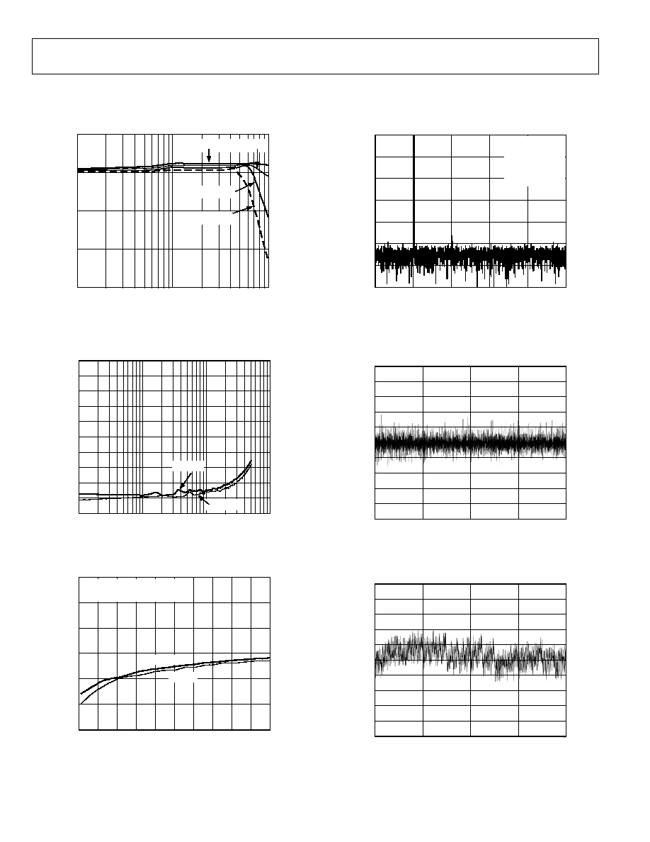
AD7440/AD7450ATYPICAL PERFORMANCE CHARACTERISTICS
T
A
= 25°C, f
S
= 1 MSPS, f
SCLK
= 18 MHz, unless otherwise noted.
75
70
65
60
55
10
100
1000
03051-A
-
007
FREQUENCY (kHz)
S
I
NAD (dB)
V
DD
= 5.25V
V
DD
= 4.75V
V
DD
= 3.6V
V
DD
= 2.7V
Figure 7. AD7450A SINAD vs. Analog Input Frequency for Various
Supply Voltages
0
100
90
80
70
60
50
40
30
20
10
10
1000
100
10000
03051-A
-
008
FREQUENCY (kHz)
CMRR (dB)
V
DD
= 3V
V
DD
= 5V
Figure 8. CMRR vs. Frequency for V
DD
= 5 V and 3 V
0
120
20
40
60
80
100
0
100
200
300
400
500
600
700
800
900 1000
03051-A
-
009
SUPPLY RIPPLE FREQUENCY (kHz)
P
S
RR (dB)
100mV p-p SINEWAVE ON V
DD
NO DECOUPLING ON V
DD
V
DD
= 3V
V
DD
= 5V
Figure 9. PSRR vs. Supply Ripple Frequency without Supply Decoupling
0
140
120
100
80
60
40
20
0
100
200
300
400
500
03051-A
-
010
FREQUENCY (kHz)
S
NR (dB)
8192 POINT FFT
f
SAMPLE
= 1MSPS
f
IN
= 100kSPS
SINAD = +71.7dB
THD = 82dB
SFDR = 83dB
Figure 10. AD7450A Dynamic Performance with V
DD
= 5 V
1.0
1.0
0.8
0.6
0.4
0.2
0
0.2
0.4
0.6
0.8
0
1024
2048
3072
4096
03051-A
-
011
CODE
DNL E
RROR (LS
B
)
Figure 11. Typical DNL for the AD7450A for V
DD
= 5 V
1.0
1.0
0.8
0.6
0.4
0.2
0
0.2
0.4
0.6
0.8
0
1024
2048
3072
4096
03051-A
-
012
CODE
INL E
RROR (LS
B
)
Figure 12. Typical INL for the AD7450A for V
DD
= 5 V
AD7440/AD7450A
Rev. B | Page 13 of 28
3.0
1.0
0.5
0
0.5
1.0
1.5
2.0
2.5
0
0.5
1.0
1.5
2.0
2.5
3.0
3.5
03051-A
-
013
V
REF
(V)
CHANGE
IN DNL (LS
B
)
POSITIVE DNL
NEGATIVE DNL
Figure 13. Change in DNL vs. V
REF
for the AD7450A for V
DD
= 5 V
2.5
1.0
0.5
0
0.5
1.0
1.5
2.0
0
0.5
1.0
1.5
2.0
2.2
2.5
03051-A
-
014
V
REF
(V)
CHANGE
IN DNL (LS
B
)
POSITIVE DNL
NEGATIVE DNL
Figure 14. Change in DNL vs. V
REF
for the AD7450A for V
DD
= 3 V
5
5
4
3
2
1
0
1
2
3
4
0
0.5
1.0
1.5
2.5
2.0
3.0
3.5
03051-A
-
015
V
REF
(V)
CHANGE
IN INL (LS
B
)
POSITIVE INL
NEGATIVE INL
Figure 15. Change in INL vs. V
REF
for the AD7450A for V
DD
= 5 V
2.5
2.0
1.5
1.0
0.5
0
0.5
1.0
1.5
2.0
0
0.5
1.0
1.5
2.0
2.2
2.5
03051-A
-
016
V
REF
(V)
CHANGE
IN INL (LS
B
)
POSITIVE INL
NEGATIVE INL
Figure 16. Change in INL vs. V
REF
for the AD7450A for V
DD
= 3 V
8
0
1
2
3
4
5
6
7
0
0.5
1.0
1.5
2.0
2.5
3.0
3.5
03051-A
-
017
V
REF
(V)
ZE
RO-CODE
E
RROR (LS
B
)
V
DD
= 5V
V
DD
= 3V
Figure 17. Change in Zero-Code Error vs. Reference Voltage for
V
DD
= 5 V and 3 V for the AD7450A
12.0
7.0
7.5
8.0
8.5
9.0
9.5
10.0
10.5
11.0
11.5
0
0.5
1.0
1.5
2.0
2.5
3.0
3.5
03051-A
-
018
V
REF
(V)
E
FFE
CTIV
E
NUMBE
R OF BITS
V
DD
= 5V
V
DD
= 3V
Figure 18. Change in ENOB vs. Reference Voltage for V
DD
= 5 V and 3 V
for the AD7450A
AD7440/AD7450A
Rev. B | Page 14 of 28
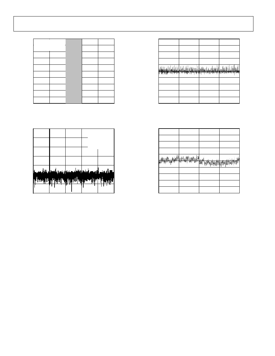
10,000
0
1,000
2,000
3,000
4,000
5,000
6,000
7,000
8,000
9,000
2044
2045
2046
2047
2048
2049
03051-A
-
019
CODE
10,000
CODES
V
IN+
= V
IN
10,000 CONVERSIONS
f
S
= 1MSPS
Figure 19. Histogram of 10,000 Conversions of a DC Input for the
AD7450A with V
DD
= 5 V
0
140
120
100
80
60
40
20
0
100
200
300
400
500
03051-A
-
020
FREQUENCY (kHz)
S
NR (dB)
8192 POINT FFT
f
SAMPLE
= 1MSPS
f
IN
= 100kHz
SINAD = +61.6dB
THD = 81.7dB
SFDR = 83.1dB
Figure 20. AD7440 Dynamic Performance with V
DD
= 5 V
0.5
0.5
0.4
0.3
0.2
0.1
0
0.1
0.2
0.3
0.4
0
256
512
768
1024
03051-A
-
021
CODE
DNL E
RROR (LS
B
)
Figure 21. Typical DNL for the AD7440 for V
DD
= 5 V
0.5
0.5
0.4
0.3
0.2
0.1
0
0.1
0.2
0.3
0.4
0
256
512
768
1024
03051-A
-
022
CODE
INL E
RROR (LS
B
)
Figure 22. Typical INL for the AD7440 for V
DD
= 5 V
AD7440/AD7450A
Rev. B | Page 15 of 28
CIRCUIT INFORMATION
The AD7440/AD7450A are 10-bit and 12-bit fast, low power,
single-supply, successive approximation analog-to-digital
converters (ADCs). They can operate with a 5 V or 3 V power
supply and are capable of throughput rates up to 1 MSPS when
supplied with an 18 MHz SCLK. They require an external
reference to be applied to the V
REF
pin, with the value of the
reference chosen depending on the power supply and what suits
the application.
When they are operated with a 5 V supply, the maximum
reference that can be applied is 3.5 V. When they are operated
with a 3 V supply, the maximum reference that can be applied is
2.2 V (see the Reference section).
The AD7440/AD7450A have an on-chip differential track-and-
hold amplifier, a successive approximation (SAR) ADC, and a
serial interface, housed in either an 8-lead SOT-23 or an MSOP
package. The serial clock input accesses data from the part and
provides the clock source for the successive approximation
ADC. The AD7440/AD7450A feature a power-down option for
reduced power consumption between conversions. The power-
down feature is implemented across the standard serial interface
as described in the Modes of Operation section.
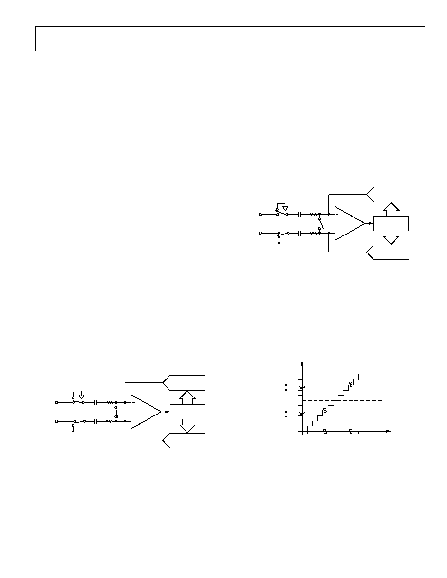
CONVERTER OPERATION
The AD7440/AD7450A are successive approximation ADCs
based around two capacitive DACs. Figure 23 and Figure 24
show simplified schematics of the ADC in acquisition and
conversion phase, respectively. The ADC is comprised of
control logic, an SAR, and two capacitive DACs. In Figure 23
(acquisition phase), SW3 is closed, SW1 and SW2 are in
Position A, the comparator is held in a balanced condition,
and the sampling capacitor arrays acquire the differential
signal on the input.
03051-A
-
023
V
IN+
V
IN
A
B
SW1
SW3
COMPARATOR
CONTROL
LOGIC
CAPACITIVE
DAC
CAPACITIVE
DAC
C
S
C
S
V
REF
SW2
B
A
Figure 23. ADC Acquisition Phase
When the ADC starts a conversion (Figure 24), SW3 opens and
SW1 and SW2 move to Position B, causing the comparator to
become unbalanced. Both inputs are disconnected once the
conversion begins. The control logic and the charge redistri-
bution DACs are used to add and subtract fixed amounts of
charge from the sampling capacitor arrays to bring the compar-
ator back into a balanced condition. When the comparator is
rebalanced, the conversion is complete. The control logic
generates the ADC's output code. The output impedances of the
sources driving the V
IN+
and the V
IN
pins must be matched;
otherwise, the two inputs have different settling times, resulting
in errors.
03051-A
-
024
V
IN+
V
IN
A
B
SW1
SW3
COMPARATOR
CONTROL
LOGIC
CAPACITIVE
DAC
CAPACITIVE
DAC
C
S
C
S
V
REF
SW2
B
A
Figure 24. ADC Conversion Phase
ADC TRANSFER FUNCTION
The output coding for the AD7440/AD7450A is twos
complement. The designed code transitions occur at successive
LSB values (1 LSB, 2 LSBs, and so on). The LSB size of the
AD7450A is 2 × V
REF
/4096, and the LSB size of the AD7440 is
2 × V
REF
/1024. The ideal transfer characteristic of the
AD7440/AD7450A is shown in Figure 25.
03051-A
-
025
100...000
ANALOG INPUT
(V
IN+
V
IN
)
011...111
100...001
100...010
011...110
000...001
111...111
1 LSB
1LSB = 2
×
V
REF
/4096 AD7450A
1LSB = 2
×
V
REF
/1024 AD7440
+V
REF
1 LSB
V
REF
0 LSB
000...000
ADC CODE
Figure 25. AD7440/AD7450A Ideal Transfer Characteristic
AD7440/AD7450A
Rev. B | Page 16 of 28
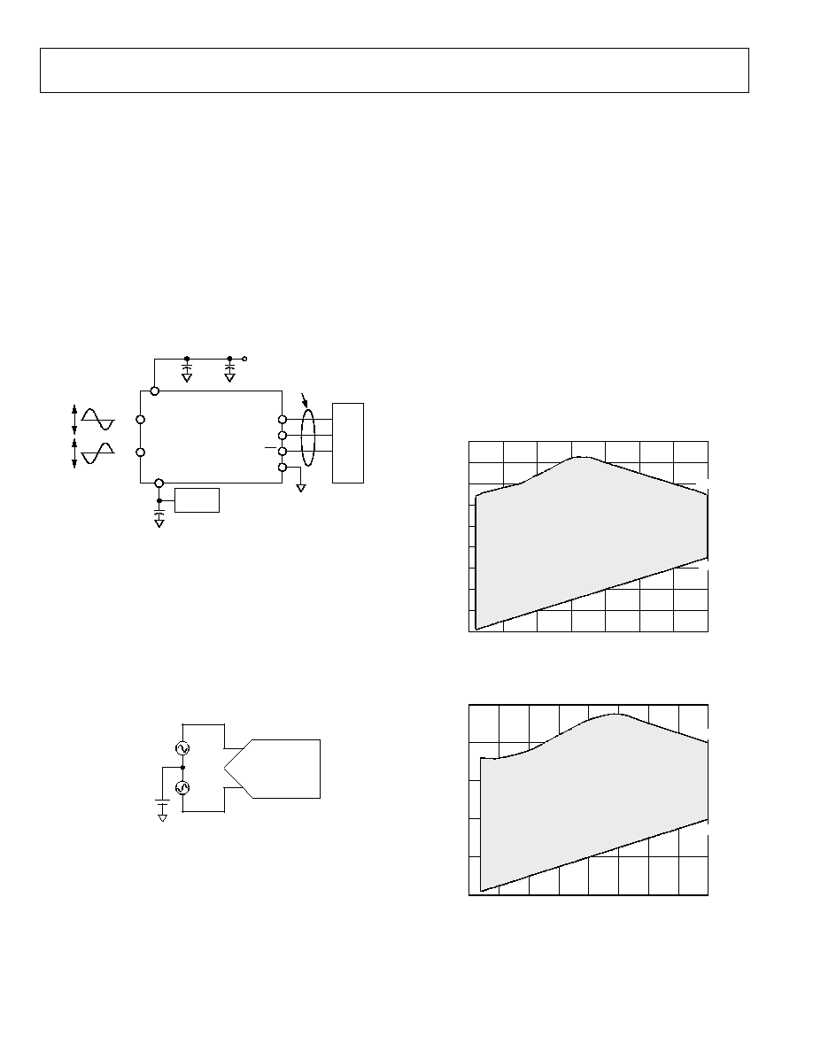
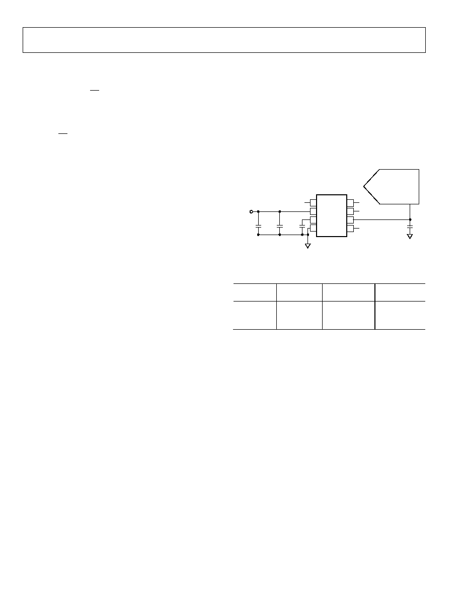
TYPICAL CONNECTION DIAGRAM
Figure 26 shows a typical connection diagram for the
AD7440/AD7450A for both 5 V and 3 V supplies. In this setup,
the GND pin is connected to the analog ground plane of the
system. The V
REF
pin is connected to either a 2.5 V or a 2 V
decoupled reference source, depending on the power supply, to
set up the analog input range. The common-mode voltage has
to be set up externally and is the value on which the two inputs
are centered. The conversion result is output in a 16-bit word
with 4 leading zeros followed by the MSB of the 12-bit or 10-bit
result. The 10-bit result of the AD7440 is followed by 2 trailing
zeros. For more details on driving the differential inputs and
setting up the common mode, refer to the Driving Differential
Inputs section.
03051-A
-
026
AD7440/
AD7450A
0.1
µ
F
0.1
µ
F
10
µ
F
V
REF
V
DD
V
IN+
SCLK
3V/5V
SUPPLY
SERIAL
INTERFACE
µ
C/
µ
P
SDATA
CS
GND
V
IN
2V/2.5V
V
REF
*CM IS THE COMMON-MODE VOLTAGE.
CM*
V
REF
p-p
CM*
V
REF
p-p
Figure 26. Typical Connection Diagram
ANALOG INPUT
The analog input of the AD7440/AD7450A is fully differential.
Differential signals have a number of benefits over single-
ended signals, including noise immunity based on the device's
common-mode rejection, improvements in distortion perfor-
mance, doubling of the device's available dynamic range, and
flexibility in input ranges and bias points. Figure 27 defines the
fully differential analog input of the AD7440/AD7450A.
03051-A
-
027
V
REF
p-p
V
IN+
V
IN
V
REF
p-p
AD7440/
AD7450A
COMMON-MODE
VOLTAGE
Figure 27. Differential Input Definitions
The amplitude of the differential signal is the difference
between the signals applied to the V
IN+
and V
IN
pins
(i.e., V
IN+
V
IN
). V
IN+
and V
IN
are simultaneously driven by two
signals each of amplitude V
REF
that are 180° out of phase. The
amplitude of the differential signal is therefore V
REF
to +V
REF
peak-to-peak (2 × V
REF
). This is true regardless of the common
mode (CM).
The common mode is the average of the two signals, that is,
(V
IN+
+ V
IN
)/2 and is therefore the voltage that the two inputs
are centered on. This results in the span of each input being
CM ± V
REF
/2. This voltage has to be set up externally, and its
range varies with V
REF
. As the value of V
REF
increases, the
common-mode range decreases. When driving the inputs with
an amplifier, the actual common-mode range is determined by
the amplifier's output voltage swing.
Figure 28 and Figure 29 show how the common-mode range
typically varies with V
REF
for both a 5 V and a 3 V power supply.
The common mode must be in this range to guarantee the
functionality of the AD7440/AD7450A.
For ease of use, the common mode can be set up to equal V
REF
,
resulting in the differential signal being ±V
REF
centered on V
REF
.
When a conversion takes place, the common mode is rejected,
resulting in a virtually noise-free signal of amplitude V
REF
to
+V
REF
, corresponding to the digital codes of 0 to 4096 in the
case of the AD7450A and 0 to 1024 in the AD7440.
4.5
4.0
3.5
3.0
2.5
2.0
1.5
1.0
0.5
0
0
0.5
1.0
1.5
2.0
2.5
3.0
3.5
03051-A
-
028
V
REF
(V)
COMMON-MODE
V
O
LTAGE
(V
)
1.75V
3.25V
COMMON-MODE RANGE
Figure 28. Input Common-Mode Range vs. V
REF
(V
DD
= 5 V and V
REF
(Max) = 3.5 V)
2.5
0.5
1.0
1.5
2.0
0
0
0.25
0.50
0.75
1.00
1.25
1.50
1.75
2.00
03051-A
-
029
V
REF
(V)
COMMON-MODE
V
O
LTAGE
(V
)
1V
2V
COMMON-MODE RANGE
Figure 29. Input Common-Mode Range vs. V
REF
(V
DD
= 3 V and V
REF
(Max) =2V)
AD7440/AD7450A
Rev. B | Page 17 of 28
Figure 30 shows examples of the inputs to V
IN+
and V
IN
for
different values of V
REF
for V
DD
= 5 V. It also gives the maximum
and minimum common-mode voltages for each reference value
according to Figure 28.
03051-A
-
030
COMMON-MODE (CM)
CM
MIN
= 1V
CM
MAX
= 4V
REFERENCE = 2V
V
IN
V
IN+
2V p-p
COMMON-MODE (CM)
CM
MIN
= 1.25V
CM
MAX
= 3.75V
REFERENCE = 2.5V
V
IN
V
IN+
2.5V p-p
Figure 30. Examples of the Analog Inputs to V
IN+
and V
IN
for
Different Values of V
REF
for V
DD
= 5 V
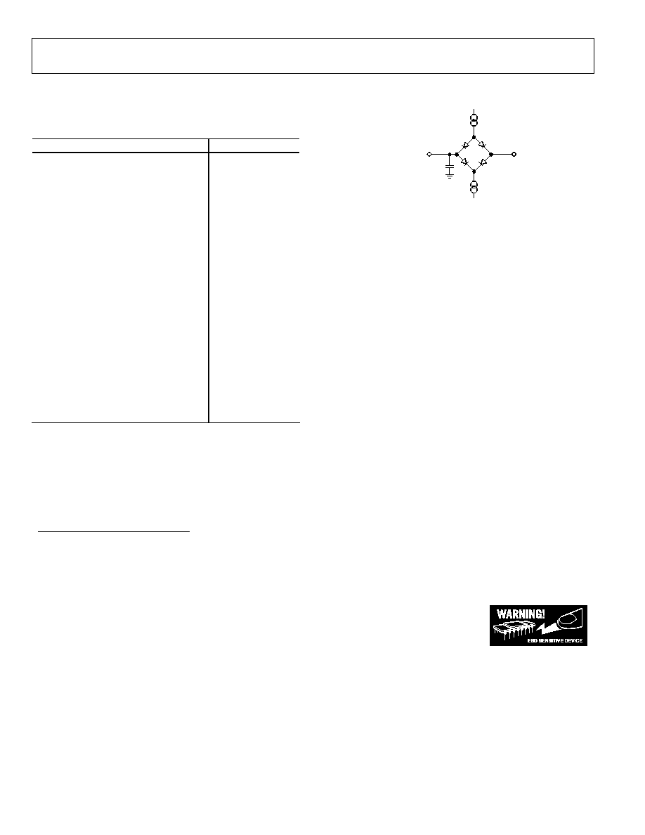
Analog Input Structure
Figure 31 shows the equivalent circuit of the analog input
structure of the AD7440/AD7450A. The four diodes provide
ESD protection for the analog inputs. Care must be taken to
ensure that the analog input signals never exceed the supply
rails by more than 300 mV. This causes these diodes to become
forward biased and start conducting into the substrate. These
diodes can conduct up to 10 mA without causing irreversible
damage to the part. The capacitors, C1 in Figure 31, are typically
4 pF and can primarily be attributed to pin capacitance. The
resistors are lumped components made up of the on resistance
of the switches. The value of these resistors is typically about
100 . The capacitors, C2, are the ADC's sampling capacitors
and have a capacitance of 16 pF typically.
03051-A
-
031
C1
C2
R1
D
D
C1
C2
R1
D
D
V
DD
V
DD
V
IN+
V
IN
Figure 31. Equivalent Analog Input Circuit
Conversion PhaseSwitches Open; Track PhaseSwitches Closed
For ac applications, removing high frequency components from
the analog input signal through the use of an RC low-pass filter
on the relevant analog input pins is recommended. In applica-
tions where harmonic distortion and signal-to-noise ratio are
critical, the analog input should be driven from a low impe-
dance source. Large source impedances significantly affect the
ac performance of the ADC. This may necessitate the use of an
input buffer amplifier. The choice of op amp is a function of the
particular application.
When no amplifier is used to drive the analog input, the source
impedance should be limited to low values. The maximum
source impedance depends on the amount of total harmonic
distortion (THD) that can be tolerated. The THD increases as
the source impedance increases, and performance degrades.
Figure 32 shows a graph of THD versus the analog input signal
frequency for different source impedances for V
DD
= 5 V.
0
100
80
60
40
20
10
100
1000
03051-A
-
032
INPUT FREQUENCY (kHz)
THD (dB)
T
A
= 25
°
C
V
DD
= 5V
R
IN
= 1k
R
IN
= 510
R
IN
= 10
R
IN
= 300
Figure 32. THD vs. Analog Input Frequency for Various Source Impedances
for V
DD
=5V
Figure 33 shows a graph of the THD versus the analog input
frequency for V
DD
of 5 V ± 5% and 3 V + 20%/10%, while
sampling at 1 MSPS with an SCLK of 18 MHz. In this case, the
source impedance is 10 .
50
90
85
80
75
70
65
60
55
10
100
1000
03051-A
-
033
INPUT FREQUENCY (kHz)
THD (dB)
T
A
= 25
°
C
V
DD
= 2.7V
V
DD
= 3.6V
V
DD
= 5.25V
V
DD
= 4.75V
Figure 33. THD vs. Analog Input Frequency for 3 V and 5 V Supply Voltages
AD7440/AD7450A
Rev. B | Page 18 of 28
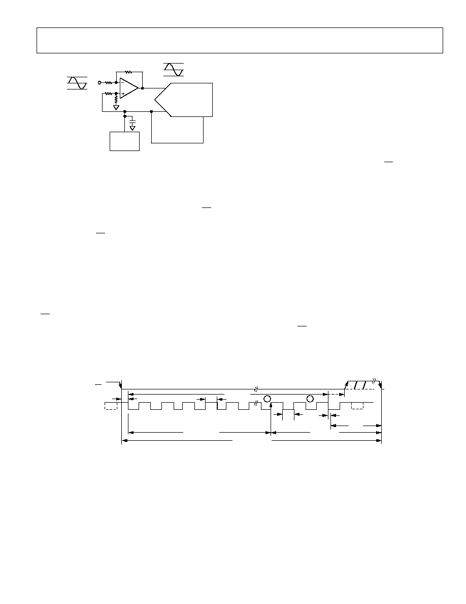
DRIVING DIFFERENTIAL INPUTS
Differential operation requires V
IN+
and V
IN
to be driven
simultaneously with two equal signals that are 180° out of
phase. The common mode must be set up externally and has a
range determined by V
REF
, the power supply, and the particular
amplifier used to drive the analog inputs (see Figure 28 and
Figure 29). Differential modes of operation with either an ac or
dc input provide the best THD performance over a wide
frequency range. Because not all applications have a signal
preconditioned for differential operation, there is often a need
to perform single-ended-to-differential conversion.
Differential Amplifier
An ideal method of applying differential drive to the
AD7440/AD7450A is to use a differential amplifier such as the
AD8138. This part can be used as a single-ended-to-differential
amplifier or as a differential-to-differential amplifier. In both
cases, the analog input needs to be bipolar. It also provides
common-mode level shifting and buffering of the bipolar input
signal. Figure 34 shows how the AD8138 can be used as a
single-ended-to-differential amplifier. The positive and negative
outputs of the AD8138 are connected to the respective inputs
on the ADC via a pair of series resistors to minimize the effects
of switched capacitance on the front end of the ADCs. The RC
low-pass filter on each analog input is recommended in ac
applications to remove high frequency components of the
analog input. The architecture of the AD8138 results in outputs
that are very highly balanced over a wide frequency range
without requiring tightly matched external components.
If the analog input source being used has zero impedance, all
four resistors (R
G
1, R
G
2, R
F
1, and R
F
2) should be the same. If
the source has a 50 impedance and a 50 termination, for
example, the value of R
G
2 should be increased by 25 to
balance this parallel impedance on the input and thus ensure
that both the positive and negative analog inputs have the same
gain (see Figure 34). The outputs of the amplifier are perfectly
matched, balanced differential outputs of identical amplitude
and are exactly 180° out of phase.
The AD8138 is specified with +3 V, +5 V, and ±5 V power
supplies, but the best results are obtained with a ±5 V supply.
The AD8132 is a lower cost device that could also be used in
this configuration with slight differences in characteristics to
the AD8138 but with similar performance and operation.
03051-A
-
034
+2.5V
GND
2.5V
AD8138
51
R
G
1
R
S
*
C*
C*
R
S
*
R
G
2
R
F
2
V
OCM
R
F
1
3.75V
V
IN+
V
IN
V
REF
2.5V
1.25V
3.75V
2.5V
1.25V
AD7440/
AD7450A
*MOUNT AS CLOSE TO THE AD7440/AD7450A AS POSSIBLE
AND ENSURE HIGH PRECISION R
S
AND C
S
ARE USED.
R
S
50
; C1nF
R
G
1 = R
F
1 = R
F
2 = 499
; R
G
2 = 523
EXTERNAL
V
REF
(2.5V)
Figure 34. Using the AD8138 as a Single-Ended-to-Differential Amplifier
AD7440/AD7450A
Rev. B | Page 19 of 28
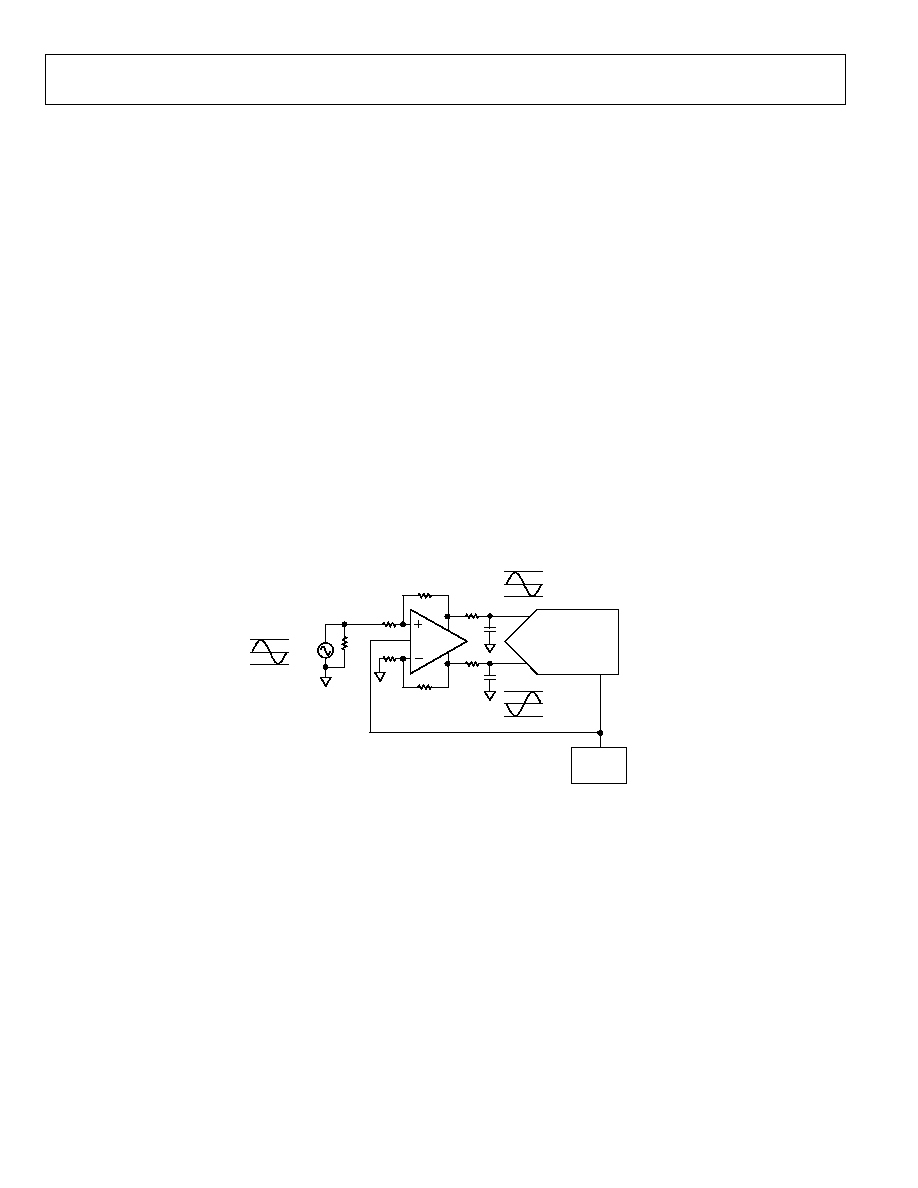
Op Amp Pair
An op amp pair can be used to directly couple a differential
signal to the AD7440/AD7450A. The circuit configurations
shown in Figure 35 and Figure 36 show how a dual op amp can
be used to convert a single-ended signal into a differential
signal for both a bipolar and unipolar input signal, respectively.
The voltage applied to Point A sets up the common-mode
voltage. In both diagrams, it is connected in some way to the
reference, but any value in the common-mode range can be
input here to set up the common mode. The AD8022 is a
suitable dual op amp that could be used in this configuration
to provide differential drive to the AD7440/AD7450A.
Take care when choosing the op amp; the selection depends on
the required power supply and system performance objectives.
The driver circuits in Figure 35 and Figure 36 are optimized for
dc coupling applications requiring best distortion performance.
The circuit configuration shown in Figure 35 converts a
unipolar, single-ended signal into a differential signal.
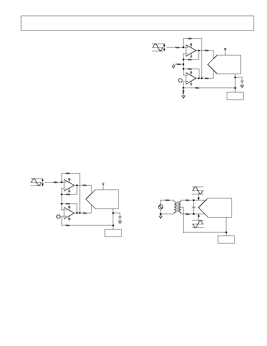
The differential op amp driver circuit in Figure 36 is configured
to convert and level shift a single-ended, ground-referenced
(bipolar) signal to a differential signal centered at the V
REF
level
of the ADC.
03051-
A-
036
V
DD
2
×
V
REF
p-p
V
REF
GND
390
220
220
220
10k
27
27
0.1
µ
F
V+
V
V+
V
A
V
IN+
V
IN
V
REF
AD7440/
AD7450A
EXTERNAL
V
REF
Figure 35. Dual Op Amp Circuit to Convert a Single-Ended Unipolar Signal
into a Differential Signal
03051-A-035
GND
V+
V
V+
V
A
V
IN+
V
DD
V
IN
V
REF
AD7440/
AD7450A
2
×
V
REF
p-p
390
220
220
220
220
10k
20k
27
27
0.1
µ
F
EXTERNAL
V
REF
Figure 36. Dual Op Amp Circuit to Convert a Single-Ended Bipolar Signal into
a Differential Signal
RF Transformer
An RF transformer with a center tap offers a good solution for
generating differential inputs in systems that do not need to
be dc-coupled. Figure 37 shows how a transformer is used for
single-ended-to-differential conversion. It provides the benefits
of operating the ADC in the differential mode without contri-
buting additional noise and distortion. An RF transformer also
has the benefit of providing electrical isolation between the
signal source and the ADC. A transformer can be used for most
ac applications. The center tap is used to shift the differential
signal to the common-mode level required; in this case, it is
connected to the reference so the common-mode level is the
value of the reference.
03051-A
-
037
R
R
C
3.75V
2.5V
1.25V
3.75V
2.5V
1.25V
R
V
IN+
V
IN
V
REF
AD7440/
AD7450A
EXTERNAL
V
REF
Figure 37. Using an RF Transformer to Generate Differential Inputs
AD7440/AD7450A
Rev. B | Page 20 of 28
DIGITAL INPUTS
The digital inputs applied to the device are not limited by the
maximum ratings, which limit the analog limits. Instead the
digital inputs applied, CS and SCLK, can go to 7 V and are not
restricted by the V
DD
+ 0.3 V limits as on the analog input.
The main advantage of the inputs not being restricted to the
V
DD
+ 0.3 V limit is that power supply sequencing issues are
avoided. If CS and SCLK are applied before V
DD
, there is no risk
of latch-up as there would be on the analog inputs if a signal
greater than 0.3 V was applied prior to V
DD
.
REFERENCE
An external reference source is required to supply the reference
to the device. This reference input can range from 100 mV to
3.5 V. With a 5 V power supply, the specified reference is 2.5 V
and the maximum reference is 3.5 V. With a 3 V power supply,
the specified reference is 2 V and the maximum reference is
2.2 V. In both cases, the reference is functional from 100 mV.
Ensure that, when choosing the reference value for a particular
application, the maximum analog input range (V
IN
max) is
never greater than V
DD
+ 0.3 V to comply with the maximum
ratings of the device. The following two examples calculate the
maximum V
REF
input that can be used when operating the
AD7440/AD7450A at a V
DD
of 5 V and 3 V, respectively.
Example 1
V
IN
max = V
DD
+ 0.3
V
IN
max = V
REF
+ V
REF
/2
If V
DD
= 5 V, then V
IN
max = 5.3 V.
Therefore
3 × V
REF
/2 = 5.3 V
V
REF
max = 3.5 V
Thus, when operating at V
DD
= 5 V, the value of V
REF
can range
from 100 mV to a maximum value of 3.5 V. When V
DD
= 4.75 V,
V
REF
max = 3.17 V.
Example 2
V
IN
max = V
DD
+ 0.3
V
IN
max = V
REF
+ V
REF
/2
If V
DD
= 3 V, then V
IN
max = 3.3 V.
Therefore,
3 × V
REF
/2 = 3.3 V
V
REF
max = 2.2 V
Thus, when operating at V
DD
= 3 V, the value of V
REF
can range
from 100 mV to a maximum value of 2.2 V. When V
DD
= 2.7 V,
V
REF
max = 2 V.
These examples show that the maximum reference applied to
the AD7440/AD7450A is directly dependent on the value
applied to V
DD
.
The value of the reference sets the analog input span and the
common-mode voltage range. Errors in the reference source
result in gain errors in the AD7440/AD7450A transfer function
and add to specified full-scale errors on the part. A 0.1 µF
capacitor should be used to decouple the V
REF
pin to GND.
Figure 38 shows a typical connection diagram for the V
REF
pin.
Table 6 lists examples of suitable voltage references.
03051-A
-
038
1
AD780
NC
8
2
V
IN
NC
7
3
GND
6
4
TEMP
5
OPSEL
TRIM
V
OUT
AD7440/
AD7450A*
V
REF
2.5V
NC
V
DD
NC
V
DD
NC = NO CONNECT
10nF
0.1
µ
F
0.1
µ
F
0.1
µ
F
*ADDITIONAL PINS OMITTED FOR CLARITY
Figure 38. Typical V
REF
Connection Diagram for V
DD
= 5 V
Table 6. Examples of Suitable Voltage References
Reference
Output
Voltage (V)
Initial
Accuracy (%)
Operating
Current (µA)
AD780
2.5/3
0.04
1000
ADR421
2.5
0.04
500
ADR420
2.048
0.05
500
SINGLE-ENDED OPERATION
When supplied with a 5 V power supply, the AD7440/AD7450A
can handle a single-ended input. The design of these devices is
optimized for differential operation, so with a single-ended
input, performance degrades. Linearity degrades by typically
0.2 LSB, the full-scale errors degrade typically by 1 LSB, and ac
performance is not guaranteed.
To operate the AD7440/AD7450A in single-ended mode, the
V
IN+
input is coupled to the signal source, while the V
IN
input is
biased to the appropriate voltage corresponding to the midscale
code transition. This voltage is the common mode, which is a
fixed dc voltage (usually the reference). The V
IN+
input swings
around this value and should have a voltage span of 2 × V
REF
to
make use of the full dynamic range of the part. The input signal
therefore has peak-to-peak values of common mode ±V
REF
. If
the analog input is unipolar, an op amp in a noninverting unity
gain configuration can be used to drive the V
IN+
pin. The ADC
operates from a single supply, so it is necessary to level shift
ground-based bipolar signals to comply with the input
requirements. An op amp can be configured to rescale and level
shift the ground-based bipolar signal, so it is compatible with
the selected input range of the AD7440/AD7450A (Figure 39).
AD7440/AD7450A
Rev. B | Page 21 of 28
03051-A
-
039
R
5V
2.5V
0V
+2.5V
0V
2.5V
R
R
0.1
µ
F
R
AD7440/
AD7450A
V
REF
V
IN+
V
IN
V
IN
EXTERNAL
V
REF
(2.5V)
Figure 39. Applying a Bipolar Single-Ended Input to the AD7440/AD7450A
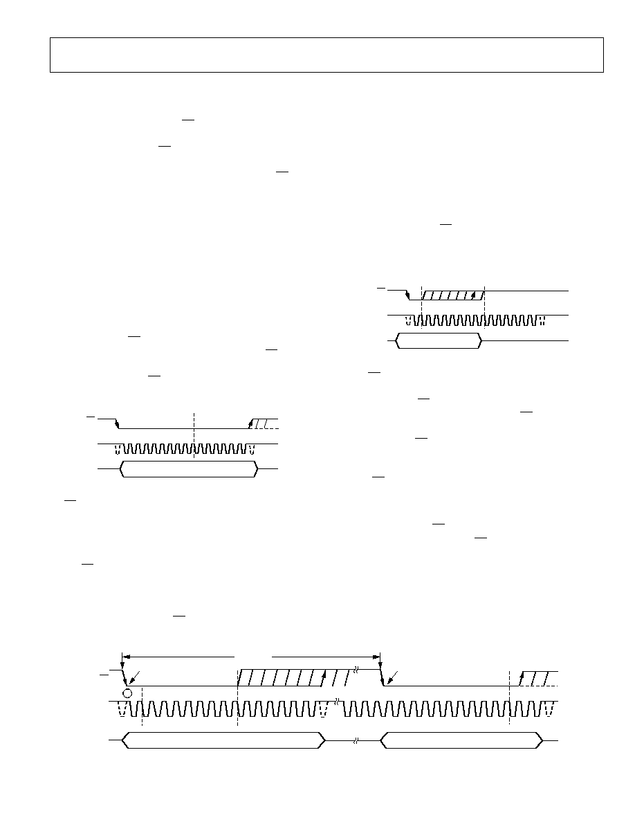
SERIAL INTERFACE
Figure 2 and Figure 3 show detailed timing diagrams for the
serial interface of the AD7450A and the AD7440, respectively.
The serial clock provides the conversion clock and also controls
the transfer of data from the devices during conversion. CS
initiates the conversion process and frames the data transfer.
The falling edge of CS puts the track-and-hold into hold mode
and takes the bus out of three-state. The analog input is sampled
and the conversion is initiated at this point. The conversion
requires 16 SCLK cycles to complete.
Once 13 SCLK falling edges have occurred, the track-and-hold
goes back into track on the next SCLK rising edge, as shown at
Point B in Figure 2 and Figure 3. On the 16th SCLK falling edge,
the SDATA line goes back into three-state. If the rising edge of
CS occurs before 16 SCLKs have elapsed, the conversion
terminates and the SDATA line goes back into three-state.
The conversion result from the AD7440/AD7450A is provided
on the SDATA output as a serial data stream. The bits are
clocked out on the falling edge of the SCLK input. The data
stream of the AD7450A consists of four leading zeros followed
by 12 bits of conversion data provided MSB first; the data
stream of the AD7440 consists of four leading zeros, followed by
the 10 bits of conversion data followed by two trailing zeros,
which is also provided MSB first. In both cases, the output
coding is twos complement.
Sixteen serial clock cycles are required to perform a conversion
and access data from the AD7440/AD7450A. CS going low
provides the first leading zero to be read in by the DSP or
microcontroller. The remaining data is then clocked out on the
subsequent SCLK falling edges beginning with the second
leading zero. Thus, the first falling clock edge on the serial clock
provides the second leading zero. The final bit in the data
transfer is valid on the 16th falling edge, having been clocked
out on the previous (15th) falling edge. Once the conversion is
complete and the data has been accessed after the 16 clock
cycles, it is important to ensure that before the next conversion
is initiated, enough time is left to meet the acquisition and
quiet time specifications (see Timing Examples 1 and 2). To
achieve 1 MSPS with an 18 MHz clock for V
DD
= 3 V and 5 V, an
18-clock burst performs the conversion and leaves enough time
before the next conversion for the acquisition and quiet time.
In applications with a slower SCLK, it may be possible to read in
data on each SCLK rising edge; that is, the first rising edge of
SCLK after the CS falling edge would have the leading zero
provided and the 15th SCLK edge would have DB0 provided.
03051-A
-
040
t
2
t
8
t
6
t
5
t
CONVERT
CS
SCLK
1
2
3
4
5
13
14
15
16
12.5(1/F
SCLK
)
t
ACQUISITION
1/THROUGHPUT
t
QUIET
10ns
B
C
Figure 40. Serial Interface Timing Example

AD7440/AD7450A
Rev. B | Page 22 of 28
Timing Example 1
Having F
SCLK
= 18 MHz and a throughput rate of 1 MSPS gives a
cycle time of
1/Throughput = 1/1,000,000 = 1 µs
A cycle consists of
t
2
+ 12.5(1/F
SCLK
) + t
ACQ
= 1 µs
Therefore, if t
2
= 10 ns
10 ns + 12.5(1/18 MHz) + t
ACQ
= 1 µs
t
ACQ
= 296 ns
This 296 ns satisfies the requirement of 290 ns for t
ACQ
.
From Figure 40, t
ACQ
comprises
2.5(1/F
SCLK
) + t
8
+ t
QUIET
where t
8
= 35 ns. This allows a value of 122 ns for t
QUIET
,
satisfying the minimum requirement of 60 ns.
Timing Example 2
Having F
SCLK
= 5 MHz and a throughput rate of 315 kSPS gives a
cycle time of
1/Throughput = 1/315,000 = 3.174 µs
A cycle consists of
t
2
+ 12.5(1/F
SCLK
) + t
ACQ
= 3.174 µs
Therefore, if t
2
is 10 ns
10 ns + 12.5(1/5 MHz) + t
ACQ
= 3.174 µs
t
ACQ
= 664 ns
This 664 ns satisfies the requirement of 290 ns for t
ACQ
.
From Figure 40, t
ACQ
comprises
2.5(1/F
SCLK
) + t
8
+ t
QUIET
where t
8
= 35 ns. This allows a value of 129 ns for t
QUIET,
satisfying the minimum requirement of 60 ns.
As in this example and with other slower clock values, the signal
may already be acquired before the conversion is complete, but
it is still necessary to leave 60 ns minimum t
QUIET
between
conversions. In Timing Example 2, the signal should be fully
acquired at approximately Point C in Figure 40.
AD7440/AD7450A
Rev. B | Page 23 of 28
MODES OF OPERATION
The operational mode of the AD7440/AD7450A is selected by
controlling the logic state of the CS signal during a conversion.
There are two possible modes of operation, normal and power
down. The point at which CS is pulled high after the conversion
has been initiated determines whether or not the device enters
power-down mode. Similarly, if already in power-down, CS
controls whether the devices return to normal operation or
remain in power-down. These modes of operation are designed
to provide flexible power management options. These options
can be chosen to optimize the power dissipation/throughput
rate ratio for differing application requirements.
NORMAL MODE
This mode is intended for fastest throughput rate performance.
The user does not have to worry about any power-up times with
the AD7440/AD7450A remaining fully powered up all the time.
Figure 41 shows the general diagram of the operation of the
AD7440/AD7450A in this mode. The conversion is initiated on
the falling edge of CS, as described in the Serial Interface
section. To ensure the part remains fully powered up, CS must
remain low until at least 10 SCLK falling edges have elapsed
after the falling edge of CS.
03051-A
-
041
1
10
CS
SCLK
SDATA
16
4 LEADING ZEROS + CONVERSION RESULT
Figure 41. Normal Mode Operation
If CS is brought high any time after the 10th SCLK falling edge,
but before the 16th SCLK falling edge, the part remains
powered up but the conversion terminates and SDATA goes
back into three-state. Sixteen serial clock cycles are required to
complete the conversion and access the complete conversion
result. CS may idle high until the next conversion or may idle
low until sometime prior to the next conversion. Once a data
transfer is complete, when SDATA has returned to three-state,
another conversion can be initiated after the quiet time, t
QUIET
,
has elapsed by again bringing CS low.
POWER-DOWN MODE
This mode is intended for use in applications where slower
throughput rates are required; either the ADC is powered down
between each conversion, or a series of conversions may be
performed at a high throughput rate and the ADC is then
powered down for a relatively long duration between these
bursts of conversions. When the AD7440/AD7450A are in the
power-down mode, all analog circuitry is powered down. To
enter power-down mode, the conversion process must be
interrupted by bringing CS high anywhere after the second
falling edge of SCLK and before the 10th falling edge of SCLK,
as shown in Figure 42.
03051-A
-
042
1
10
SCLK
SDATA
THREE-STATE
2
CS
Figure 42. Entering Power-Down Mode
Once CS has been brought high in this window of SCLKs, the
part enters power-down, the conversion that was initiated by
the falling edge of CS is terminated, and SDATA goes back into
three-state. The time from the rising edge of CS to SDATA
three-state enabled is never greater than t
8
(refer to the Timing
Specifications). If CS is brought high before the second SCLK
falling edge, the part remains in normal mode and does not
power down. This avoids accidental power-down due to glitches
on the CS line.
In order to exit this mode of operation and power up the
AD7440/AD7450A again, a dummy conversion is performed.
On the falling edge of CS, the device begins to power up and
continues to power up as long as CS is held low until after the
falling edge of the 10th SCLK. The device is fully powered up
after 1 µs has elapsed and, as shown in Figure 43, valid data
results from the next conversion.
03153-A
-
031
CS
SCLK
SDATA
1
10
16
1
10
16
A
THIS PART IS FULLY POWERED
UP WITH V
IN
FULLY ACQUIRED
PART BEGINS
TO POWER UP
INVALID DATA
VALID DATA
t
POWER-UP
Figure 43. Exiting Power-Down Mode

AD7440/AD7450A
Rev. B | Page 24 of 28
If CS is brought high before the 10th falling edge of SCLK, the
AD7440/AD7450A again goes back into power-down. This
avoids accidental power-up due to glitches on the CS line or an
inadvertent burst of eight SCLK cycles while CS is low. So
although the device may begin to power up on the falling edge
of CS, it again powers down on the rising edge of CS as long as
it occurs before the 10th SCLK falling edge.
POWER-UP TIME
The power-up time of the AD7440/AD7450A is typically 1 µs,
which means that with any frequency of SCLK up to 18 MHz,
one dummy cycle is always sufficient to allow the device to
power up. Once the dummy cycle is complete, the ADC is fully
powered up and the input signal is acquired properly. The quiet
time, t
QUIET
, must still be allowed from the point at which the
bus goes back into three-state after the dummy conversion to
the next falling edge of CS.
When running at the maximum throughput rate of 1 MSPS, the
AD7440/AD7450A power up and acquire a signal within
±0.5 LSB in one dummy cycle, 1 µs. When powering up from
the power-down mode with a dummy cycle, as in Figure 43, the
track-and-hold, which was in hold mode while the part was
powered down, returns to track mode after the first SCLK edge
the part receives after the falling edge of CS. This is shown as
Point A in Figure 43.
Although at any SCLK frequency one dummy cycle is sufficient
to power up the device and acquire V
IN
, it does not mean that a
full dummy cycle of 16 SCLKs must always elapse to power up
the device and acquire V
IN
fully; 1 µs is sufficient to power up
the device and acquire the input signal.
For example, if a 5 MHz SCLK frequency was applied to the
ADC, the cycle time would be 3.2 µs (1/(5 MHz) ×16). In one
dummy cycle, 3.2 µs, the part would be powered up and V
IN
acquired fully. However, after 1 µs with a 5 MHz SCLK, only five
SCLK cycles would have elapsed. At this stage, the ADC would
be fully powered up and the signal acquired. So in this case, the
CS can be brought high after the 10th SCLK falling edge and
brought low again after a time, t
QUIET
, to initiate the conversion.
When power supplies are first applied to the device, the ADC
may power up in either power-down mode or normal mode.
Because of this, it is best to allow a dummy cycle to elapse to
ensure the part is fully powered up before attempting a valid
conversion. Likewise, if the user wants the part to power up in
power-down mode, the dummy cycle may be used to ensure the
device is in power-down by executing a cycle such as the one
shown in Figure 42.
Once supplies are applied to the AD7440/AD7450A, the power-
up time is the same as that when powering up from power-
down mode. It takes about 1 µs to power up fully if the part
powers up in normal mode. It is not necessary to wait 1 µs
before executing a dummy cycle to ensure the desired mode of
operation. Instead, the dummy cycle can occur directly after
power is supplied to the ADC. If the first valid conversion is
then performed directly after the dummy conversion, ensure
that adequate acquisition time has been allowed.
As mentioned earlier, when powering up from the power-down
mode, the part returns to track mode upon the first SCLK edge
applied after the falling edge of CS. However, when the ADC
powers up initially after supplies are applied, the track-and-hold
is already in track mode. Assuming the user has the facility to
monitor the ADC supply current, this means the ADC powers
up in the desired mode of operation, and thus a dummy cycle is
not required to change mode. A dummy cycle is therefore not
required to place the track-and-hold into track mode.
POWER VS. THROUGHPUT RATE
By using the power-down mode on the AD7440/AD7450A
when not converting, the average power consumption of the
ADC decreases at lower throughput rates. Figure 44 shows how,
as the throughput rate is reduced, the device remains in its
power-down state longer and the average power consumption is
reduced accordingly for both 5 V and 3 V power supplies.
For example, if the AD7440/AD7450A are operated in
continuous sampling mode with a throughput rate of 100 kSPS
and an SCLK of 18 MHz, and the device is placed in power-
down mode between conversions, the power consumption is
calculated as follows:
Power Dissipation during Normal Operation = 9.25 mW max
(for V
DD
= 5 V)
If the power-up time is one dummy cycle (1 µs), and the
remaining conversion time is another cycle (1 µs), the
AD7440/AD7450A can be said to dissipate 9.25 mW for 2 µs
1
during each conversion cycle.
If the throughput rate = 100 kSPS, the cycle time = 10 µs and
the average power dissipated during each cycle is
(2/10) × 9.25mW = 1.85 mW.
For the same scenario, if V
DD
= 3 V, the power dissipation during
normal operation is 4 mW max.
The AD7440/AD7450A can now be said to dissipate 4 mW for
2 µs
1
during each conversion cycle.
1
This figure assumes a very short time to enter power-down mode. This
increases as the burst of clocks used to enter this mode is increased.
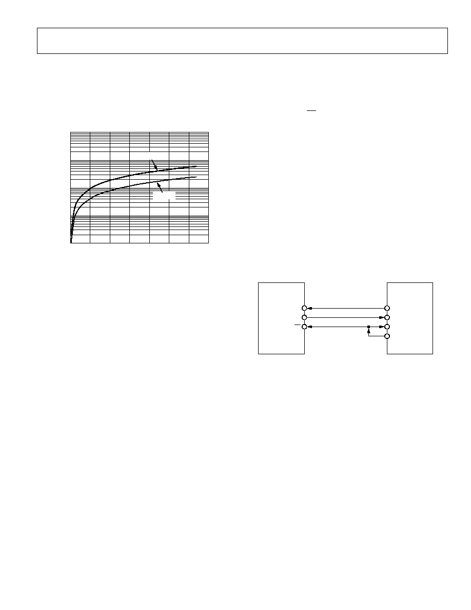
AD7440/AD7450A
Rev. B | Page 25 of 28
Thus, the average power dissipated during each cycle with a
throughput rate of 100 kSPS is (2/10) × 4 mW = 0.8 mW.
This is how the power numbers in Figure 44 are calculated.
For throughput rates above 320 kSPS, it is recommended to
reduce the serial clock frequency for best power performance.
03051-A
-
044
THROUGHPUT (kSPS)
100
0
350
P
O
WE
R (mW)
0.01
50
100
150
200
250
300
0.1
1
10
V
DD
= 5V
V
DD
= 3V
Figure 44. Power vs. Throughput Rate for Power-Down Mode
MICROPROCESSOR AND DSP INTERFACING
The serial interface on the AD7440/AD7450A allows the parts
to be directly connected to many different microprocessors.
This section explains how to interface the AD7440/AD7450A
with some of the more common microcontroller and DSP serial
interface protocols.
AD7440/AD7450A to ADSP-21xx
The ADSP-21xx family of DSPs is interfaced directly to the
AD7440/AD7450A without any glue logic required.
The SPORT control register should be set up as follows:
TFSW = RFSW = 1
Alternate framing
INVRFS = INVTFS = 1
Active low frame signal
DTYPE = 00
Right-justify data
SLEN = 1111
16-bit data-words
ISCLK = 1
Internal serial clock
TFSR = RFSR = 1
Frame every word
IRFS = 0
ITFS = 1
To implement power-down mode, SLEN should be set to 1001
to issue an 8-bit SCLK burst.
The connection diagram is shown in Figure 45. The ADSP-21xx
has the TFS and RFS of the SPORT tied together, with TFS set
as an output and RFS set as an input. The DSP operates in
alternate framing mode and the SPORT control register is set
up as described. The frame synchronization signal generated on
the TFS is tied to CS and, as with all signal processing
applications, equidistant sampling is necessary. However in this
example, the timer interrupt is used to control the sampling rate
of the ADC; under certain conditions, equidistant sampling may
not be achieved.
The timer registers, for example, are loaded with a value that
provides an interrupt at the required sample interval. When an
interrupt is received, a value is transmitted with TFS/DT (ADC
control word). The TFS is used to control the RFS and therefore
the reading of data. The frequency of the serial clock is set in
the SCLKDIV register. When the instruction to transmit with
TFS is given (AX0 = TX0), the state of the SCLK is checked. The
DSP waits until the SCLK has gone high, low, and high again
before starting transmission. If the timer and SCLK values are
chosen such that the instruction to transmit occurs on or near
the rising edge of SCLK, then the data may be transmitted or it
may wait until the next clock edge.
03051-A
-
045
AD7440/
AD7450A*
ADSP-21xx*
SCLK
DR
RFS
TFS
SCLK
SDATA
CS
*ADDITIONAL PINS REMOVED FOR CLARITY
Figure 45. Interfacing to the ADSP-21xx
For example, the ADSP-2111 has a master clock frequency of
16 MHz. If the SCLKDIV register is loaded with the value 3, an
SCLK of 2 MHz is obtained and eight master clock periods
elapse for every SCLK period. If the timer registers are loaded
with the value 803, then 100.5 SCLKs occur between interrupts
and subsequently between transmit instructions. This situation
results in nonequidistant sampling as the transmit instruction is
occurring on a SCLK edge. If the number of SCLKs between
interrupts is a whole integer figure of N, equidistant sampling is
implemented by the DSP.
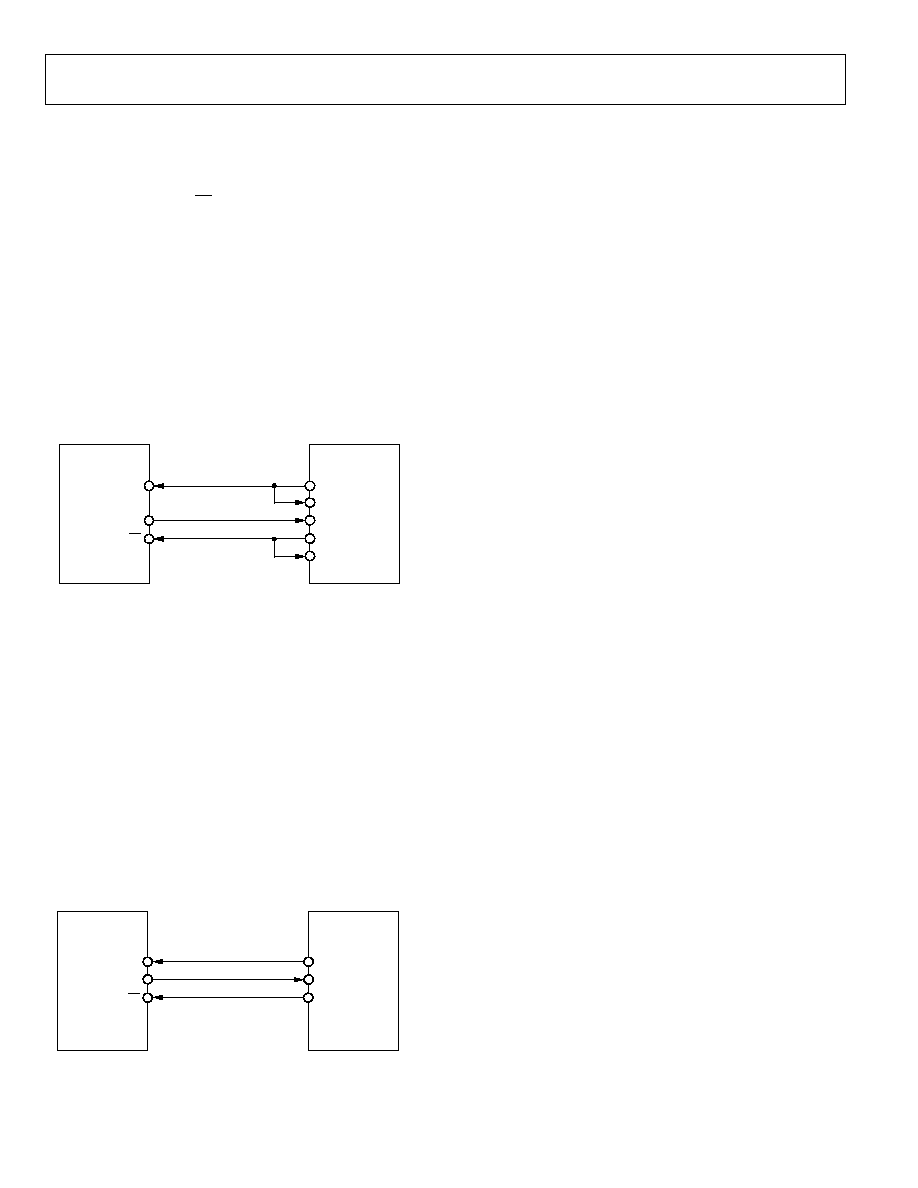
AD7440/AD7450A
Rev. B | Page 26 of 28
AD7440/AD7450A to TMS320C5x/C54x
The serial interface on the TMS320C5x/C54x uses a continuous
serial clock and frame synchronization signals to synchronize
the data transfer operations with peripheral devices like the
AD7440/AD7450A. The CS input allows easy interfacing
between the TMS320C5x/C54x and the AD7440/AD7450A
without any glue logic required. The serial port of the
TMS320C5x/C54x is set up to operate in burst mode with
internal CLKx (Tx serial clock) and FSx (Tx frame sync). The
serial port control register (SPC) must have the following setup:
FO = 0, FSM = 1, MCM = 1, and TxM = 1. The format bit, FO,
may be set to 1 to set the word length to eight bits in order to
implement the power-down mode on the AD7440/AD7450A.
The connection diagram is shown in Figure 46. For signal
processing applications, it is imperative that the frame
synchronization signal from the TMS320C5x/C54x provide
equidistant sampling.
AD7440/
AD7450A*
TMS320C5x/
C54x*
CLKx
DR
FSx
FSR
SCLK
SDATA
CS
CLKR
03051-A
-
046
*ADDITIONAL PINS REMOVED FOR CLARITY
Figure 46. Interfacing to the TMS320C5x/C54
AD7440/AD7450A to DSP56xxx
The connection diagram in Figure 47 shows how the device can
be connected to the synchronous serial interface (SSI) of the
DSP56xxx family of DSPs from Motorola. The SSI is operated in
synchronous mode (SYN bit in CRB = 1) with internally
generated 1-word frame sync for both Tx and Rx (Bits FSL1 = 0
and FSL0 = 0 in CRB). Set the word length to 16 by setting Bits
WL1 = 1 and WL0 = 0 in CRA. To implement power-down
mode on the AD7440/AD7450A, the word length can be
changed to 8 bits by setting Bits WL1 = 0 and WL0 = 0 in CRA.
For signal processing applications, it is imperative that the
frame synchronization signal from the DSP56xxx provide
equidistant sampling.
AD7440/
AD7450A*
03051-A
-
047
DSP56xxx*
SCLK
SRD
SR2
SCLK
SDATA
CS
*ADDITIONAL PINS REMOVED FOR CLARITY
Figure 47. Interfacing to the DSP56xxx
GROUNDING AND LAYOUT HINTS
The printed circuit board that houses the AD7440/AD7450A
should be designed so that the analog and digital sections are
separated and confined to certain areas of the board. This
facilitates the use of ground planes that can be easily separated.
A minimum etch technique is generally best for ground planes
as it gives the best shielding. Digital and analog ground planes
should be joined in only one place, a star ground point
established as close to the GND pin on the AD7440/AD7450A
as possible. Avoid running digital lines under the devices
because this couples noise onto the die. The analog ground
plane should be allowed to run under the AD7440/AD7450A to
avoid noise coupling. The power supply lines to the
AD7440/AD7450A should use as large a trace as possible to
provide low impedance paths and reduce the effects of glitches
on the power supply line.
Fast switching signals like clocks should be shielded with digital
ground to avoid radiating noise to other sections of the board,
and clock signals should never run near the analog inputs.
Avoid crossover of digital and analog signals. Traces on opposite
sides of the board should run at right angles to each other. This
reduces the effects of feedthrough through the board. A micro-
strip technique is by far the best but is not always possible with
a double-sided board.
In this technique, the component side of the board is dedicated
to ground planes while signals are placed on the solder side.
Good decoupling is also important. All analog supplies should
be decoupled with 10 µF tantalum capacitors in parallel with
0.1 µF capacitors to GND. To achieve the best from these
decoupling components, they must be placed as close as
possible to the device.
EVALUATING THE AD7440/AD7450A
PERFORMANCE
The evaluation board package includes a fully assembled and
tested evaluation board, documentation, and software for
controlling the board from a PC via the evaluation board
controller. The evaluation board controller can be used in
conjunction with the AD7440/AD7450A evaluation board, as
well as many other Analog Devices evaluation boards ending
with the CB designator, to demonstrate and evaluate the ac and
dc performance of the AD7440/AD7450A.
The software allows the user to perform ac (fast Fourier
transform) and dc (histogram of codes) tests on the device. See
the AD7440/AD7450A application note that accompanies the
evaluation kit for more information.
AD7440/AD7450A
Rev. B | Page 27 of 28
OUTLINE DIMENSIONS
1
3
5
6
2
8
4
7
2.90 BSC
PIN 1
1.60 BSC
1.95
BSC
0.65 BSC
0.38
0.22
0.15 MAX
1.30
1.15
0.90
SEATING
PLANE
1.45 MAX
0.22
0.08
0.60
0.45
0.30
8°
4°
0°
2.80 BSC
COMPLIANT TO JEDEC STANDARDS MO-178BA
Figure 48. 8-Lead Small Outline Transistor Package [SOT-23]
(RT-8)
Dimensions shown in millimeters
0.80
0.60
0.40
8°
0°
4
8
5
4.90
BSC
PIN 1
0.65 BSC
3.00
BSC
SEATING
PLANE
0.15
0.00
0.38
0.22
1.10 MAX
3.00
BSC
COPLANARITY
0.10
0.23
0.08
COMPLIANT TO JEDEC STANDARDS MO-187AA
Figure 49. 8-Lead Mini Small Outline Package [MSOP]
(RM-8)
Dimensions shown in millimeters
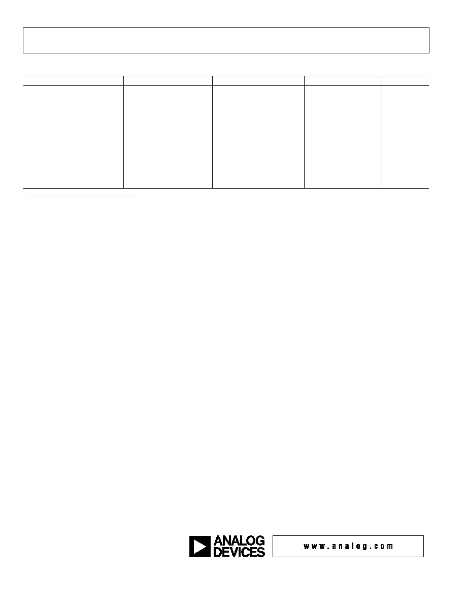
AD7440/AD7450A
Rev. B | Page 28 of 28
ORDERING GUIDE
Model
Temperature Range
Linearity Error (LSB)
1
Package Option
2
Branding
AD7440BRT-REEL7
40°C to +85°C
±0.5
RT-8
CTB
AD7440BRT-R2
40°C to +85°C
±0.5
RT-8
CTB
AD7440BRM
40°C to +85°C
±0.5
RM-8
CTB
AD7440BRM-REEL7
40°C to +85°C
±0.5
RM-8
CTB
AD7450ABRT-REEL7
40°C to +85°C
±1
RT-8
CSB
AD7450ABRT-R2
40°C to +85°C
±1
RT-8
CSB
AD7450ABRM
40°C to +85°C
±1
RM-8
CSB
AD7450ABRM-REEL7
40°C to +85°C
±1
RM-8
CSB
EVAL-AD7440CB
3
Evaluation Board
EVAL-AD7450ACB
3
Evaluation Board
EVAL-CONTROL BRD2
4
Controller Board
1
Linearity error here refers to integral nonlinearity error.
2
RT = SOT-23; RM = MSOP
3
This can be used as a standalone evaluation board or in conjunction with the evaluation board controller for evaluation/demonstration purposes.
4
Evaluation board controller. This board is a complete unit allowing a PC to control and communicate with all Analog Devices' evaluation boards ending in the CB
designator. For a complete evaluation kit, order the ADC evaluation board (that is, the EVAL-AD7450ACB or EVAL-AD7440CB), the EVAL-CONTROL BRD2, and a 12 V ac
transformer. See the AD7440/AD7450A application note that accompanies the evaluation kit for more information.
©2004 Analog Devices, Inc. All rights reserved. Trademarks and
registered trademarks are the property of their respective owners.
C03051-0-2/04(B)
Document Outline