 | –≠–ª–µ–∫—Ç—Ä–æ–Ω–Ω—ã–π –∫–æ–º–ø–æ–Ω–µ–Ω—Ç: IRF7401 | –°–∫–∞—á–∞—Ç—å:  PDF PDF  ZIP ZIP |
Document Outline
- FEATURES
- APPLICATIONS
- GENERAL DESCRIPTION
- FUNCTIONAL BLOCK DIAGRAM
- SPECIFICATIONS
- ABSOLUTE MAXIMUM RATINGS
- ESD RATINGS
- ORDERING GUIDE
- PIN CONFIGURATION
- PIN FUNCTION DESCRIPTIONS
- Typical Performance Characteristics
- APPLICATION NOTES
- Principle of Operation
- Signal Flow Diagram
- Thermistor Setup
- Design Example 1
- Design Example 2
- DAC Resolution for TEMPSET
- Thermistor Fault and Temperature Lock Indications
- Setting the Switching Frequency
- Soft Start on Power-Up
- Shutdown Mode
- Compensation Loop
- Using the TEC Controller ADN8830 with a Wave Locker
- Using TEMPOUT to Measure Temperature
- Setting the Maximum TEC Voltage and Current
- Output Driver Amplifiers
- Inductor Selection
- Design Example 3
- Design Example 4
- PWM Output Filter Requirements
- Calculating PWM Output Ripple Voltage
- External FET Requirements
- Calculating Power Dissipation and Efficiency
- Layout Considerations
- Power Supply Ripple
- Setting Maximum Output Current and Short-Circuit Protection
- Design Example 5
- Using an RTD for Temperature Sensing
- Using a Resistive Load as a Heating Element
- Suggested Pad Layout for CP-32 Package
- OUTLINE DIMENSIONS
- Revision History
REV. C
Information furnished by Analog Devices is believed to be accurate and
reliable. However, no responsibility is assumed by Analog Devices for its
use, nor for any infringements of patents or other rights of third parties that
may result from its use. No license is granted by implication or otherwise
under any patent or patent rights of Analog Devices. Trademarks and
registered trademarks are the property of their respective owners.
One Technology Way, P.O. Box 9106, Norwood, MA 02062-9106, U.S.A.
Tel: 781/329-4700
www.analog.com
Fax: 781/326-8703
© 2003 Analog Devices, Inc. All rights reserved.
ADN8830
Thermoelectric Cooler Controller
FEATURES
High Efficiency
Small Size: 5 mm 5 mm LFCSP
Low Noise: <0.5% TEC Current Ripple
Long-Term Temperature Stability: 0.01 C
Temperature Lock Indication
Temperature Monitoring Output
Oscillator Synchronization with an External Signal
Clock Phase Adjustment for Multiple Controllers
Programmable Switching Frequency up to 1 MHz
Thermistor Failure Alarm
Maximum TEC Voltage Programmability
APPLICATIONS
Thermoelectric Cooler (TEC) Temperature Control
Resistive Heating Element Control
Temperature Stabilization Substrate (TSS) Control
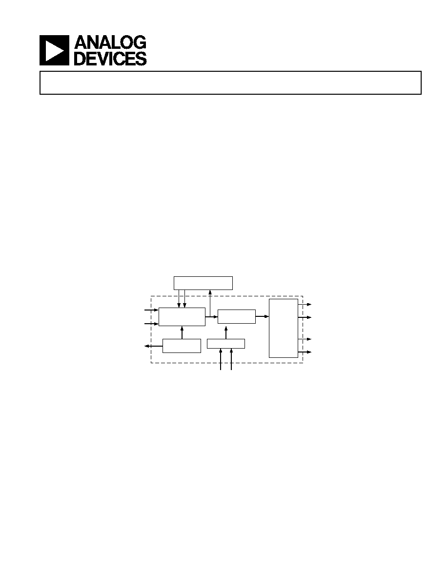
FUNCTIONAL BLOCK DIAGRAM
PID COMPENSATION
NETWORK
TEMPERATURE
MEASUREMENT
AMPLIFIER
PWM
CONTROLLER
FROM
THERMISTOR
TEMPERATURE
SET
INPUT
VOLTAGE
REFERENCE
V
REF
OSCILLATOR
FREQUENCY/PHASE
CONTROL
P-CHANNEL
(UPPER MOSFET)
N-CHANNEL
MOSFET
DRIVERS
P-CHANNEL
(LOWER MOSFET)
N-CHANNEL
GENERAL DESCRIPTION
The ADN8830 is a monolithic controller that drives a thermo-
electric cooler (TEC) to stabilize the temperature of a laser diode
or a passive component used in telecommunications equipment.
This device relies on a negative temperature coefficient (NTC)
thermistor to sense the temperature of the object attached to the
TEC. The target temperature is set with an analog input voltage
either from a DAC or an external resistor divider.
The loop is stabilized by a PID compensation amplifier with
high stability and low noise. The compensation network can be
adjusted by the user to optimize temperature settling time. The
component values for this network can be calculated based on
the thermal transfer function of the laser diode or obtained
from the lookup table given in the Application Notes section.
Voltage outputs are provided to monitor both the temperature of
the object and the voltage across the TEC. A voltage reference
of 2.5 V is also provided.

REV. C
≠2≠
ADN8830≠SPECIFICATIONS
(@ V
DD
= 3.3 V to 5.0 V, V
GND
= 0 V, T
A
= 25 C, T
SET
= 25 C, using typical application
configuration as shown in Figure 1, unless otherwise noted.)
Parameter
Symbol
Conditions
Min
Typ
Max
Unit
TEMPERATURE STABILITY
Long-Term Stability
Using 10 k
thermistor with
= ≠4.4% at 25
∞C
0.01
∞C
PWM OUTPUT DRIVERS
Output Transition Time
t
R
, t
F
C
L
= 3,300 pF
20
ns
Nonoverlapping Clock Delay
50
65
ns
Output Resistance
R
O
(N1, P1)
I
L
= 50 mA
6
Output Voltage Swing
OUT A
V
LIM
= 0 V
0
V
DD
V
Output Voltage Ripple
OUT A
f
CLK
= 1 MHz
0.2
%
Output Current Ripple
I
TEC
f
CLK
= 1 MHz
0.2
%
LINEAR OUTPUT AMPLIFIER
Output Resistance
R
O, P2
I
OUT
= 2 mA
85
R
O, N2
I
OUT
= 2 mA
178
Output Voltage Swing
OUT B
0
V
DD
V
POWER SUPPLY
Power Supply Voltage
V
DD
3.0
5.5
V
Power Supply Rejection Ratio
PSRR
V
DD
= 3.3 V to 5 V, V
TEC
= 0 V
80
92
dB
≠40
∞C T
A
+85∞C
60
dB
Supply Current
I
SY
PWM not switching
8
12
mA
≠40
∞C T
A
+85∞C
15
mA
Shutdown Current
I
SD
Pin 10 = 0 V
5
µA
Soft-Start Charging Current
I
SS
15
µA
Undervoltage Lockout
V
OLOCK
Low-to-high threshold
2.0
2.7
V
ERROR AMPLIFIER
Input Offset Voltage
V
OS
V
CM
= 1.5 V
50
250
µV
Gain
A
V, IN
20
V/V
Input Voltage Range
V
CM
0.2
2.0
V
Common-Mode Rejection Ratio
CMRR
0.2 V < V
CM
< 2.0 V
58
68
dB
≠40
∞C T
A
+85∞C
55
dB
Open-Loop Input Impedance
R
IN
1
G
Gain-Bandwidth Product
GBW
2
MHz
REFERENCE VOLTAGE
Reference Voltage
V
REF
I
REF
< 2 mA
2.37
2.47
2.57
V
OSCILLATOR
Synchronization Range
f
CLK
Pin 25 connected to external clock
200
1,000
kHz
Oscillator Frequency
f
CLK
Pin 24 = V
DD
; (R = 150 k
;
800
1,000
1,250
kHz
Pin 25 = GND)
LOGIC CONTROL
*
Logic Low Input Threshold
0.2
V
Logic High Input Threshold
3
V
Logic Low Output Level
0.2
V
Logic High Output Threshold
V
DD
≠ 0.2
V
*Logic inputs meet typical CMOS I/O conditions for source/sink current (~1
µA).
Specifications subject to change without notice.
REV. C
ADN8830
≠3≠
CAUTION
ESD (electrostatic discharge) sensitive device. Electrostatic charges as high as 4000 V readily
accumulate on the human body and test equipment and can discharge without detection. Although the
ADN8830 features proprietary ESD protection circuitry, permanent damage may occur on devices
subjected to high energy electrostatic discharges. Therefore, proper ESD precautions are recommended
to avoid performance degradation or loss of functionality.
ABSOLUTE MAXIMUM RATINGS
*
Supply Voltage . . . . . . . . . . . . . . . . . . . . . . . . . . . . . . . . . . . 6 V
Input Voltage . . . . . . . . . . . . . . . . . . . . . . . GND to V
S
+ 0.3 V
Storage Temperature Range . . . . . . . . . . . . . ≠65
∞C to +150∞C
Operating Temperature Range . . . . . . . . . . . . ≠40
∞C to +85∞C
Operating Junction Temperature . . . . . . . . . . . . . . . . . . 125
∞C
Lead Temperature Range (Soldering, 10 sec) . . . . . . . . 300
∞C
ESD RATINGS
883 (Human Body) Model . . . . . . . . . . . . . . . . . . . . . . 1.0 kV
*Stresses above those listed under Absolute Maximum Ratings may cause perma-
nent damage to the device. This is a stress rating only; functional operation of the
device at these or any other conditions above those listed in the operational
sections of this specification is not implied. Exposure to absolute maximum rating
conditions for extended periods may affect device reliability.
PIN CONFIGURATION
PIN 1
INDICATOR
TOP VIEW
24 COMPOSC
23 PGND
22 N1
21 P1
THERMFAULT 1
THERMIN 2
SD 3
32 NC
20 PVDD
19 OUT A
18 COMPSWIN
17 COMPSWOUT
OUT B 9
N2 10
P2 11
TEMPCTL 12
COMPFB 13
COMPOUT 1
4
VL
I
M
15
VTEC 16
TEMPSET 4
TEMPLOCK 5
NC 6
VREF 7
AVDD 8
31 TEMPOUT
30 AGND
29 PHASE
28 SYNCOUT
27 SOFTSTART
26 FREQ
25 SYNCIN
ADN8830
NC = NO CONNECT
Package Type
JA
*
JC
Unit
32-Lead LFCSP (ACP)
35
10
∞C/W
*
JA
is specified for worst-case conditions, i.e.,
JA
is specified for a device
soldered in a 4-layer circuit board for surface-mount packages.
ORDERING GUIDE
Model
Temperature Range
Package Description
Package Option
ADN8830ACP
≠40
∞C to +85∞C
32-Lead Lead Frame Chip Scale Package (LFCSP)
CP-32-1
ADN8830ACP-REEL
≠40
∞C to +85∞C
32-Lead Lead Frame Chip Scale Package (LFCSP)
CP-32-1
ADN8830ACP-REEL7
≠40
∞C to +85∞C
32-Lead Lead Frame Chip Scale Package (LFCSP)
CP-32-1
ADN8830-EVAL
Evaluation Board

REV. C
≠4≠
ADN8830
PIN FUNCTION DESCRIPTIONS
Pin No.
Mnemonic
Type
Description
1
THERMFAULT
Digital Output
Indicates an Open or Short-Circuit Condition from Thermistor.
2
THERMIN
Analog Input
Thermistor Feedback Input.
3
SD
Digital Input
Puts Device into Low Current Shutdown Mode. Active low.
4
TEMPSET
Analog Input
Target Temperature Input.
5
TEMPLOCK
Digital Output
Indicates when Thermistor Temperature is within
±0.1∞C of Target Tem-
perature as Set by TEMPSET Voltage.
6
NC
No Connection, except as Noted in the Application Notes Section.
7
VREF
Analog Output
2.5 V Reference Voltage.
8
AVDD
Power
Power for Nondriver Sections. 3.0 V min; 5.5 V max.
9
OUT B
Analog Input
Linear Output Feedback. Will typically connect to TEC+ pin of TEC.
10
N2
Analog Output
Drives Linear Output External NMOS Gate.
11
P2
Analog Output
Drives Linear Output External PMOS Gate.
12
TEMPCTL
Analog Output
Output of Error Amplifier. Connects to COMPFB through feedforward
section of compensation network.
13
COMPFB
Analog Input
Feedback Summing Node of Compensation Amplifier. Connects to
TEMPCTL and COMPOUT through compensation network.
14
COMPOUT
Analog Output
Output of Compensation Amplifier. Connects to COMPFB through feed-
back section of compensation network.
15
VLIM
Analog Input
Sets Maximum Voltage across TEC.
16
VTEC
Analog Output
Indicates Relative Voltage across the TEC. The 1.5 V corresponds to 0 V
across TEC. The 3.0 V indicates maximum output voltage, maximum heat
transfer through TEC.
17
COMPSWOUT
Analog Output
Compensation for Switching Amplifier.
18
COMPSWIN
Analog Input
Compensation for Switching Amplifier. Capacitor connected between
COMPSWIN and COMPSWOUT.
19
OUT A
Analog Input
PWM Output Feedback. Will typically connect to TEC≠ pin of TEC.
20
PVDD
Power
Power for Output Driver Sections. 3.0 V min; 5.5 V max.
21
P1
Digital Output
Drives PWM Output External PMOS Gate.
22
N1
Digital Output
Drives PWM Output External NMOS Gate.
23
PGND
Ground
Power Ground. External NMOS devices connect to PGND. Can be
connected to digital ground as noise sensitivity at this node is not critical.
24
COMPOSC
Analog Input
Connect as Indicated in the Application Notes Section.
25
SYNCIN
Digital Input
Optional Clock Input. If not connected, clock frequency set by FREQ pin.
26
FREQ
Analog Input
Sets Switching Frequency.
27
SOFTSTART
Analog Input
Controls Initialization Time for ADN8830 with Capacitor to Ground.
28
SYNCOUT
Digital Output
Phase Adjusted Clock Output. Phase set from PHASE pin. Can be used to
drive SYNCIN of other ADN8830 devices.
29
PHASE
Analog Input
Sets Switching and SYNCOUT Clock Phase Relative to SYNCIN Clock.
30
AGND
Ground
Analog Ground. Should be low noise for highest accuracy.
31
TEMPOUT
Analog Output
Indication of Thermistor Temperature.
32
NC
No Connection.
REV. C
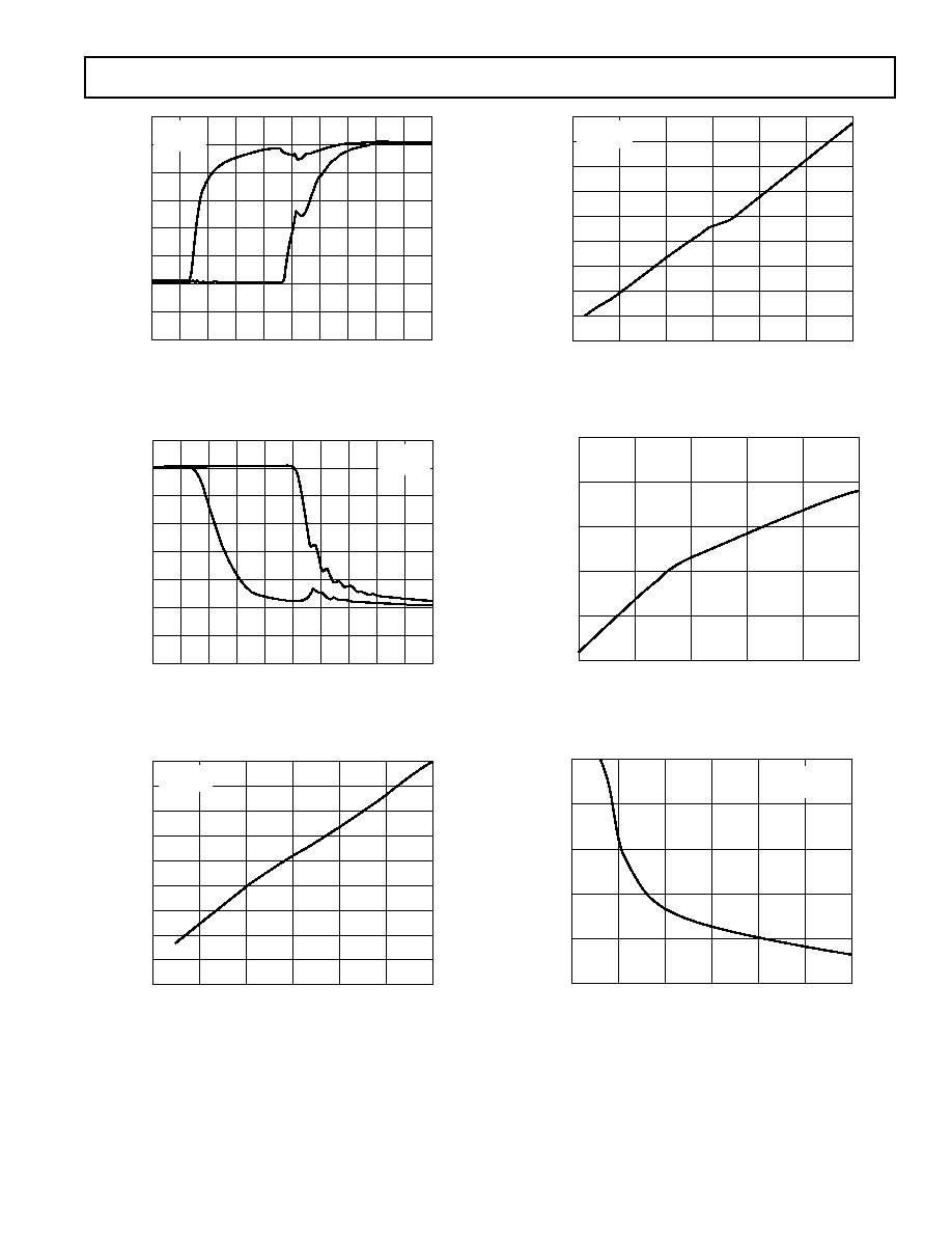
Typical Performance Characteristics≠ADN8830
≠5≠
TIME (20ns/DIV)
0
0
0
0
VO
LTA
GE (1V/DIV)
0
0
0
0
0
0
0
0
P1
N1
V
DD
= 5V
T
A
= 25 C
TPC 1. N1 and P1 Rise Time
TIME (20ns/DIV)
0
0
0
0
VO
LTA
GE (1V/DIV)
0
0
0
0
0
0
0
0
V
DD
= 5V
T
A
= 25 C
P1
N1
TPC 2. N1 and P1 Fall Time
360
320
0
PHASE SHIFT (Degrees)
160
120
80
40
240
200
280
VPHASE (V)
2.4
0.4
0.8
1.2
1.6
2.0
0
SYNC IN = 1MHz
T
A
= 25 C
TPC 3. Clock Phase Shift vs. Phase Voltage
320
0
PHASE SHIFT (Degrees)
160
120
80
40
240
200
280
VPHASE (V)
2.4
0.4
0.8
1.2
1.6
2.0
0
SYNC IN = 200kHz
T
A
= 25 C
360
TPC 4. Clock Phase Shift vs. Phase Voltage
TEMPERATURE ( C)
2.480
2.475
2.455
≠40
85
≠15
V
REF
(
V)
10
35
60
2.470
2.465
2.460
TPC 5. V
REF
vs. Temperature
R
FREQ
(k )
1,000
800
0
0
1,500
250
500
750
1,000
1,250
600
400
200
V
DD
= 5V
T
A
= 25 C
SWITCHING FREQ
UENCY (kHz)
TPC 6. Switching Frequency vs. R
FREQ
REV. C
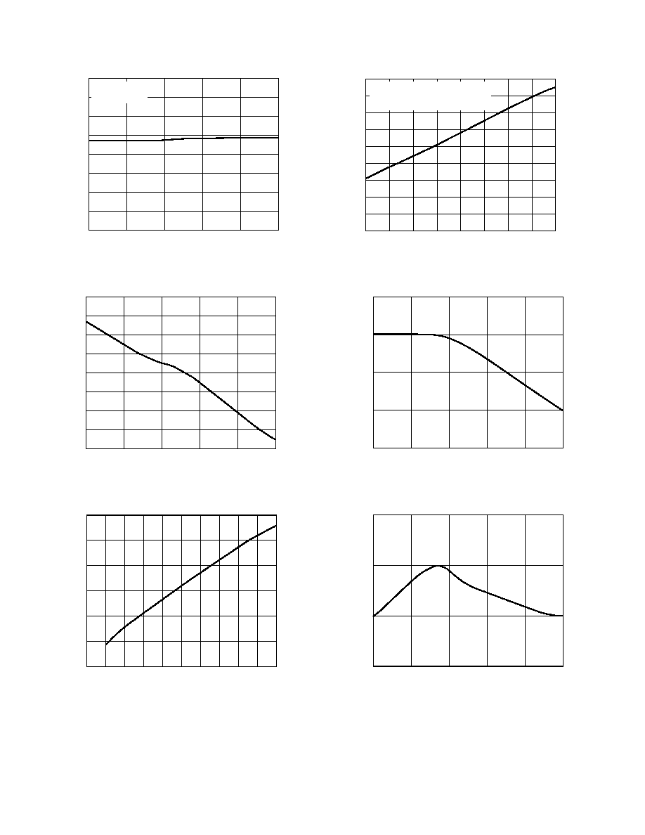
≠6≠
ADN8830
TEMPERATURE ( C)
1,000
920
≠40
85
≠15
SWITCHING FREQ
UENCY (kHz)
10
35
60
980
960
940
930
990
970
950
V
DD
= 5V
R
FREQ
= 150k
TPC 7. Switching Frequency vs. Temperature
TEMPERATURE ( C)
70
30
≠40
85
≠15
OFFSET V
O
L
T
A
GE
(
V)
10
35
60
55
45
35
65
60
50
40
TPC 8. Offset Voltage vs. Temperature
COMMON-MODE VOLTAGE (V)
200
≠100
≠400
0
2.0
0.2
OFFSET V
O
L
T
A
GE
(
V)
0.4
0.6
0.8
1.0
1.2
1.4
1.6
1.8
100
0
≠200
≠300
TPC 9. Offset Voltage vs. Common-Mode Voltage
SWITCHING FREQUENCY (kHz)
200
1,000
300
400
500
600
700
800
900
45
40
0
SUPPL
Y CURRENT (mA)
20
15
10
5
30
25
35
V
DD
= 5V
T
A
= 25 C
USING CIRCUIT SHOWN IN FIGURE 1
TPC 10. Supply Current vs. Switching Frequency
TEMPERATURE ( C)
2.06
2.02
≠40
85
≠15
THERM F
A
UL
T UPPER
THRESHOLD (V)
10
35
60
2.04
2.03
2.05
TPC 11. Open Thermistor Fault Threshold vs. Temperature
TEMPERATURE ( C)
0.26
0.23
≠40
85
≠15
THERM F
A
UL
T LO
WER
THRESHOLD (V)
10
35
60
0.25
0.24
TPC 12. Short Thermistor Fault Threshold vs.
Temperature
REV. C
ADN8830
≠7≠
APPLICATION NOTES
Principle of Operation
The ADN8830 is a controller for a TEC and is used to set and
stabilize the temperature of the TEC. A voltage applied to the
input of the ADN8830 corresponds to a target temperature
setpoint. The appropriate current is then applied to the TEC
to pump heat either to or away from the object whose tem-
perature is being regulated. The temperature of the object is
measured by a thermistor and is fed back to the ADN8830 to
correct the loop and settle the TEC to the appropriate final
temperature. For best stability, the thermistor should be mounted
in close proximity to the object. In most laser diode modules,
the TEC and thermistor are already mounted in the unit and
are used to regulate the temperature of the laser diode.
A complete TEC controller solution requires:
∑ A precision input amplifier stage to accurately measure the
difference between the target and object temperatures.
∑ A compensation amplifier to optimize the stability and
temperature settling time.
∑ A high output current stage. Because of the high output
currents involved, a TEC controller should operate with
high efficiency to minimize the heat generated from
power dissipation.
In addition, an effective controller should operate down to 3.3 V
and have an indication of when the target temperature has been
reached. The ADN8830 accomplishes all of these requirements
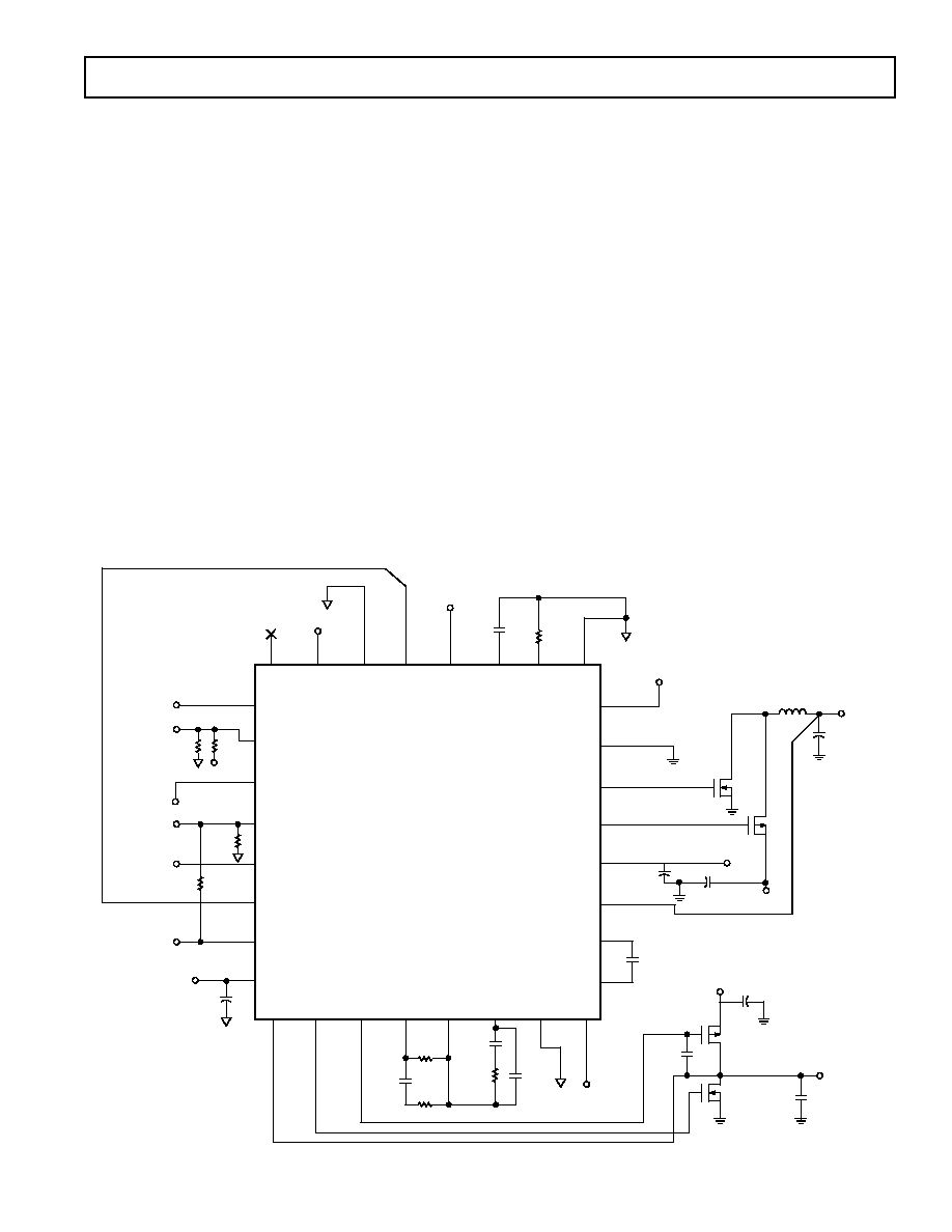
with a minimum of external components. Figure 1 shows a
reference design for a typical application.
Temperature is monitored by connecting the measurement
thermistor to a precision amplifier, called the error amplifier,
with a simple resistor divider. This voltage is compared against
the temperature set input voltage, creating an error voltage that
is proportional to their difference. To maintain accurate wave-
length and power from the laser diode, this difference voltage
must be as accurate as possible. For this reason, self-correction
auto-zero amplifiers are used in the input stage of the ADN8830,
providing a maximum offset voltage of 250
µV over time and
temperature. This results in final temperature accuracy within
±0.01∞C in typical applications, eliminating the ADN8830 as an
error source in the temperature control loop. A logic output is
provided at TEMPLOCK to indicate when the target temperature
has been reached.
The output of the error amplifier is then fed into a compensa-
tion amplifier. An external network consisting of a few resistors
and capacitors is connected around the compensation amplifier.
This network can be adjusted by the user to optimize the step
THERMFAULT
THERMIN
RTH
10k
@25 C
R2
7.68k
0.1%
VREF
C8
10 F
3.3V
VREF
TEMPLOCK
TEMPSET
R3
10k
0.1%
R4
7.68k
0.1%
VTEC
9
10
11
12
13
14
15
16
C9
10 F
R6
100k
R5
205k
C11
1 F
R7
1M
24
23
22
21
20
19
18
17
3.3V
ADN8830
C5
10nF
3.3V
TEC+
C7
10 F
Q3
FDW2520C-A
Q4
FDW2520C-B
C4
22 F
CDE ESRD
3.3V
Q2
FDW2520C-A
TEC≠
C3
10 F
L1
4.7 H
COILCRAFT
DO3316-472
Q1
FDW2520C-B
32
31
30
29
28
27
26
25
C1
0.1 F
R1
150k
SYNCOUT
TEMPOUT
3.3V
C6
2.2nF
C10
330pF
3.3V
C12
3.3nF
C2
22 F
CDE ESRD
1
2
3
4
5
6
7
8
Figure 1. Typical Application Schematic
REV. C
≠8≠
ADN8830
response of the TEC's temperature either in terms of settling time
or maximum current change. Details of how to adjust the compen-
sation network are given in the Compensation Loop section.
The ADN8830 can be easily integrated with a wavelength locker
for fine-tune temperature adjustment of the laser diode for a
specific wavelength. This is a useful topology for tunable wave-
length lasers. Details are highlighted in the Using the TEC
Controller ADN8830 with a Wave Locker section.
The TEC is driven differentially using an H-bridge configura-
tion to maximize the output voltage swing. The ADN8830
drives external transistors that are used to provide current to the
TEC. These transistors can be selected by the user based on the
maximum output current required for the TEC. The maximum
voltage across the TEC can be set through use of the VLIM pin
on the ADN8830.
To further improve the power efficiency of the system, one side
of the H-bridge uses a switched output. Only one inductor and
one capacitor are required to filter out the switching frequency.
The output voltage ripple is a function of the output inductor
and capacitor and the switching frequency. For most applica-
tions, a 4.7
µH inductor, 22 µF capacitor, and switching frequency
of 1 MHz maintains less than
±0.5% worst-case output voltage
ripple across the TEC. The other side of the H-bridge does not
require any additional circuitry.
The oscillator section of the ADN8830 controls the switched
output section. A single resistor sets the switching frequency
from 100 kHz to 1 MHz. The clock output is available at the
SYNCOUT pin and can be used to drive another ADN8830
device by connecting to its SYNCIN pin. The phase of the
clock is adjusted by a voltage applied to the PHASE pin, which
can be set by a simple resistor divider. Phase adjustment allows
two or more ADN8830 devices to operate from the same clock
frequency and not have all outputs switch simultaneously, which
could create an excessive power supply ripple. Details of how to
adjust the clock frequency and phase are given in the Setting the
Switching Frequency section.
For effective indication of a catastrophic system failure, the
ADN8830 alerts to open-circuit or short-circuit conditions from the
thermistor, preventing an erroneous and potentially damaging
temperature correction from occurring. With some additional
external circuitry, output overcurrent detection can be imple-
mented to provide warning in the event of a TEC short-circuit
failure. This circuit is highlighted in the Setting Maximum
Output Current and Short-Circuit Protection section.
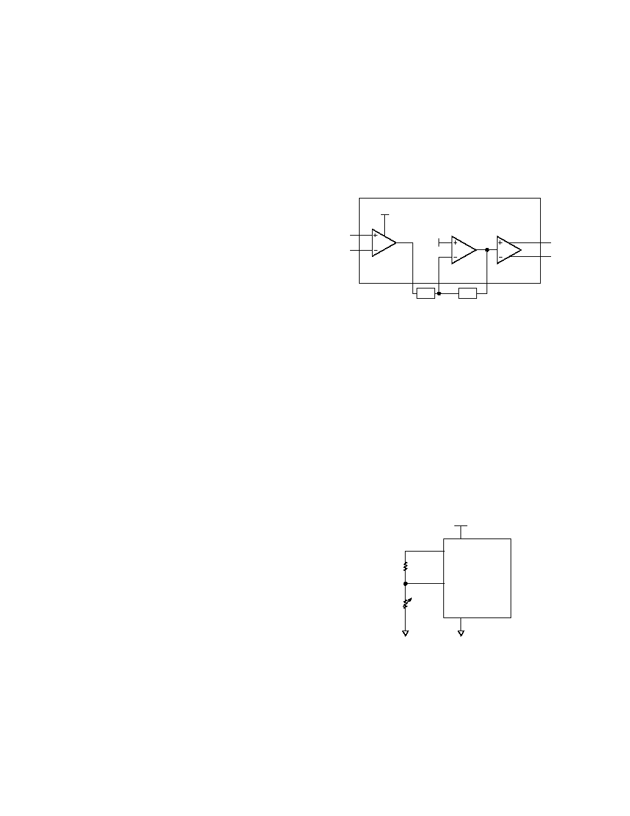
Signal Flow Diagram
Figure 2 shows the signal flow diagram through the ADN8830.
The input amplifier is fixed with a gain of 20. The voltage at
TEMPCTL can be expressed as
TEMPCTL
TEMPSET
THERMIN
=
◊
(
)
+
20
1 5
≠
.
(1)
When the temperature is settled, the thermistor voltage will be
equal to the TEMPSET voltage, and the output of the input
amplifier will be 1.5 V.
The voltage at TEMPCTL is then fed into the compensation
amplifier whose frequency response is dictated by the compen-
sation network. Details on the compensation amplifier can be
found in the Compensation Loop section. When configured as a
simple integrator or PID loop, the dc forward gain of the
compensation section is equal to the open-loop gain of the
compensation amplifier, which is over 80 dB or 10,000. The
output from the compensation loop at COMPOUT is then fed
to the linear amplifier. The output of the linear amplifier at
OUT B is fed with COMPOUT into the PWM amplifier whose
output is OUT A. These two outputs provide the voltage drive
directly to the TEC. Including the external transistors, the gain of
the differential output section is fixed at 4. Details on the output
amplifiers can be found in the Output Driver Amplifiers section.
1.5V
INPUT
AMPLIFIER
A
V
= 20
COMPENSATION
AMPLIFIER
A
V
= Z2/Z1
1.5V
Z1
A
V
= 4
PWM/LINEAR
AMPLIFIERS
OUT A
OUT B
Z2
TEMPSET
THERMIN
4
2
12
13
14
19
9
TEMPCTL
COMPOUT
COMPFB
Figure 2. Signal Flow Block Diagram of the ADN8830
Thermistor Setup
The temperature of the thermal object, such as a laser diode, is
detected with a negative temperature coefficient (NTC) thermistor.
The thermistor's resistance exhibits an exponential relationship to
the inverse of temperature, meaning the resistance decreases at
higher temperatures. Thus, by measuring the thermistor resistance,
temperature can be ascertained. Betatherm is a leading supplier
of NTC thermistors. Thermistor information and details can be
found at www.betatherm.com.
For this application, the resistance is measured using a voltage
divider. The thermistor is connected between THERMIN (Pin 2)
and AGND (Pin 30). Another resistor (R
X
) is connected between
VREF (Pin 7) and THERMIN (Pin 2), creating a voltage divider
for the VREF voltage. Figure 3 shows the schematic for this
configuration.
V
DD
ADN8830
8
7
2
30
R
THERM
R
X
Figure 3. Connecting a Thermistor to the ADN8830
With the thermistor connected from THERMIN to AGND, the
voltage at THERMIN will decrease as temperature increases.
To maintain the proper input-to-output polarity in this configu-
ration, OUT A (Pin 19) should connect to the TEC≠ pin on the
TEC, and OUT B (Pin 9) should connect to the VTEC+ pin.
The thermistor can also be connected from VREF to THERMIN
with R
X
connecting to ground. In this case, OUT A must connect to
TEC+ with OUT B connected to TEC≠ for proper operation.
REV. C
ADN8830
≠9≠
Although the thermistor has a nonlinear relationship to tem-
perature, near optimal linearity over a specified temperature
range can be achieved with the proper value of R
X
. First, the
resistance of the thermistor must be known, where
R
R
T
T
R
T
T
R
T
T
THERM
T
LOW
T
MID
T
HIGH
=
=
=
=
=
=
1
2
3
@
@
@
(2)
T
LOW
and T
HIGH
are the endpoints of the temperature range and
T
MID
is the average. These resistances can be found in most
thermistor data sheets. In some cases, only the coefficients
corresponding to the Steinhart-Hart equation are given. The
Steinhart-Hart equation is
1
1
1
3
T
a
b n R
c
n R
= +
( )
+
( )
[
]
(3)
where T is the absolute temperature of the thermistor in Kelvin
(K =
∞C + 273.15), and R is the resistance of the thermistor at
that temperature. Based on the coefficients a, b, and c, R
THERM
can be calculated for a given T, albeit somewhat tediously, by
solving the cubic roots of this equation
R
THERM
=
+
+
+
+
exp
≠
≠
≠
2
4
27
2
4
27
2
3
1
2
1
3
2
3
1
2
1
3
(4)
where
X
a
T
c
=
≠
1
and
=
b
c
R
X
is then found as
R
R R
R R
R R
R
R
R
X
T
T
T
T
T
T
T
T
T
=
+
+
1
2
2
3
1
3
1
3
2
2
2
≠
≠
(5)
For the best accuracy as well as the widest selection range for
resistances, R
X
should be 0.1% tolerance. Naturally, the smaller
the temperature range required for control, the more linear
the voltage divider will be with respect to temperature. The
voltage at THERMIN is
V
VREF
R
R
R
X
THERM
THERM
X
=
+
(6)
where VREF has a typical value of 2.47 V.
The ADN8830 control loop will adjust the temperature of the
TEC until V
X
equals the voltage at TEMPSET (Pin 4), which
we define as V
SET
. Target temperature can be set by
V
m T
T
V
SET
MID
XMID
=
(
)
+
≠
(7)
where T equals the target temperature, and
m
V
V
T
T
X HIGH
X LOW
HIGH
LOW
=
,
,
≠
≠
(8)
V
X
for high, mid, and low are found by using Equation 6 and
substituting R
T3
, R
T2
, and R
T1
, respectively, for R
THERM
. The
variable m is the change in V
X
with respect to temperature and
is expressed in V/
∞C.
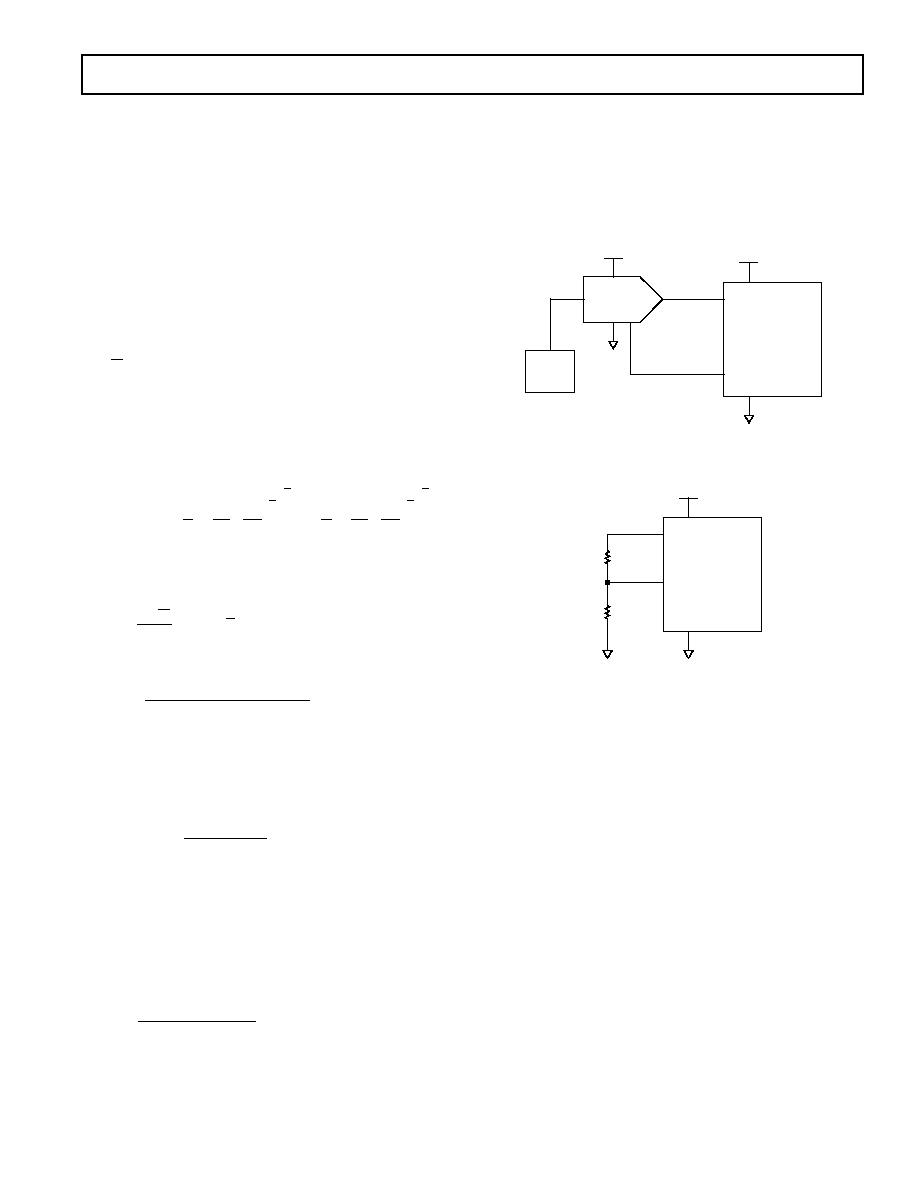
The setpoint voltage can be driven from a DAC or another
voltage source, as shown in Figure 4. The reference voltage
for the DAC should be connected to VREF (Pin 7) on the
ADN8830 to ensure best accuracy from device to device.
For a fixed target temperature, a voltage divider network can be
used as shown in Figure 5. R1 is set equal to R
X
, and R2 is
equal to the value of R
THERM
at the target temperature.
3.3V
ADN8830
8
4
7
30
AD7390
6
8
5
3.3V
7
1≠4
C
Figure 4. Using a DAC to Control the Temperature
Setpoint
3.3V
ADN8830
8
7
4
30
R2
R1
Figure 5. Using a Voltage Divider to Set a Fixed
Temperature Setpoint
Design Example 1
A laser module requires a constant temperature of 25
∞C. From
the manufacturer's data sheet, we find the thermistor in the laser
module has a value of 10 k
at 25∞C. Because the laser is not
required to operate at a range of temperatures, the value of R
X
can be set to 10 k
. TEMPSET can be set by a simple resistor
divider as shown in Figure 5, with R1 and R2 both equal to 10 k
.
Design Example 2
A laser module requires a continuous temperature control from
5
∞C to 45∞C. The manufacturer's data sheet shows the thermistor
has a value of 10 k
at 25∞C, 25.4 k at 5∞C, and 4.37 k at
45
∞C. Using Equation 5, R
X
is calculated to be 7.68 k
to yield
the most linear temperature-to-voltage conversion. A DAC
will be used to set the TEMPSET voltage.
DAC Resolution for TEMPSET
The temperature setpoint voltage to THERMIN can be set from
a DAC. The DAC must have a sufficient number of bits to achieve
adequate temperature resolution from the system. The voltage
range for THERMIN is found by multiplying the variable m
from Equation 8 by the temperature range.
THERMIN Voltage Range
m
T
T
MAX
MIN
= ◊
(
)
≠
(9)
From Design Example 2, 40
∞C of the control temperature range
is achieved with a voltage range of only 1 V.
REV. C
≠10≠
ADN8830
To eliminate the resolution of the DAC as the principal source
of system error, the step size of each bit, V
STEP
, should be lower
than the desired system resolution. A practical value for absolute
DAC resolution is the equivalent of 0.05
∞C. The value of V
STEP
should be less than the value of m from Equation 8 multiplied
by the desired temperature resolution, or
V
C
m
STEP
<
∞ ◊
0 05
.
(10)
where m is the slope of the voltage-to-temperature conversion
line, as found from Equation 8. From Design Example 2, where
m = 25 mV/
∞C, we see the DAC should have resolution better
than 1.25 mV per step.
The minimum number of bits required is then given as
Number of Bits
V
V
FS
STEP
=
( )
(
)
( )
log
≠ log
log 2
(11)
where V
FS
is the full-scale output voltage from the DAC, which
should be equal to the reference voltage from the ADN8830,
VREF = 2.47 V as given in the Specifications table for the
Reference Voltage. In this example, the minimum resolution is
11 bits. A 12-bit DAC, such as the AD7390, can be readily
found.
It is important that the full-scale voltage input to the DAC is tied
to the ADN8830 reference voltage, as shown in Figure 4. This
eliminates errors from slight variances of VREF.
Thermistor Fault and Temperature Lock Indications
Both the THERMFAULT (Pin 1) and TEMPLOCK (Pin 5)
outputs are CMOS compatible outputs that are active high.
THERMFAULT will be a logic low while the thermistor is
operating normally and will go to a logic high if a short or
open is detected at THERMIN (Pin 2). The trip voltage for
THERMFAULT is when THERMIN falls below 0.2 V or
exceeds 2.0 V. THERMFAULT provides only an indication of
a fault condition and does not activate any shutdown or protec-
tion circuitry on the ADN8830. To shut down the ADN8830, a
logic low voltage must be asserted on Pin 3, as described in the
Shutdown Mode section.
TEMPLOCK will output a logic high when the voltage at
THERMIN is within 2.5 mV of TEMPSET. This voltage can
be related to temperature by solving for m from Equation 8. For
most laser diode applications, 2.5 mV is equivalent to
±0.1∞C.
If the voltage difference between THERMIN and TEMPSET is
greater than 2.5 mV, then TEMPLOCK will output a logic low.
The input offset voltage of the ADN8830 is guaranteed to within
250
µV, which for most applications is within ±0.01∞C.
Setting the Switching Frequency
The ADN8830 has an internal oscillator to generate the switch-
ing frequency for the output stage. This oscillator can be either
set in free-run mode or synchronized to an external clock
signal. For free-run operation, SYNCIN (Pin 25) should be
connected to ground and COMPOSC (Pin 24) should be
connected to AVDD. The switching frequency is then set by a
single resistor connected from FREQ (Pin 26) to ground.
Table I shows R
FREQ
for some common switching frequencies.
Table I. Switching Frequencies vs. R
FREQ
f
SWITCH
R
FREQ
100 kHz
1.5 M
250 kHz
600 k
500 kHz
300 k
750 kHz
200 k
1 MHz
150 k
For other frequencies, the value for this resistor, R
FREQ
, should
be set to
R
f
FREQ
SWITCH
=
◊
150
10
9
(12)
where f
SWITCH
is the switching frequency in Hz.
Higher switching frequencies reduce the voltage ripple across
the TEC. However, high switch frequencies will create more
power dissipation in the external transistors. This is due to the
more frequent charging and discharging of the transistors' gate
capacitances. If large transistors are needed for a high output
current application, faster switching frequencies could reduce
the overall power efficiency of the circuit. This is covered in
detail in the Calculating Power Dissipation and Efficiency section.
The switching frequency of the ADN8830 can be synchronized
with an external clock by connecting the clock signal to SYNCIN
(Pin 25). Pin 24 should also be connected to an R-C network, as
shown in Figure 6. This network is simply used to compensate a
PLL to lock on to the external clock. To ensure the quickest
synchronization lock-in time, R
FREQ
should be set to 1.5 M
.
ADN8830
FREQ
COMPOSC
1.5M
26
24
0.1 F
1k
1nF
Figure 6. Using an R-C Network on Pin 24 with
an External Clock
The relative phase of the ADN8830 internal oscillator compared
to the external clock signal can be adjusted. This is accomplished
by adjusting the voltage to PHASE (Pin 29) according to TPCs 3
and 4. The phase shift versus voltage can be approximated as
Phase Shift
V
VREF
PHASE
∞ =
∞ ◊
360
(13)
where V
PHASE
is the voltage at Pin 29, and VREF has a typical
value of 2.47 V.
To ensure the oscillator operates correctly, V
PHASE
should remain
higher than 100 mV and lower than 2.3 V. This is required for
either internal clock or external synchronization operation. A
resistor divider from VREF to ground can establish this voltage
easily, although any voltage source, such as a DAC, could be used
as well. If phase is not a consideration, for example with a single
ADN8830 being used, Pin 29 can be tied to Pin 6, which pro-
vides a 1.5 V reference voltage.
REV. C
ADN8830
≠11≠
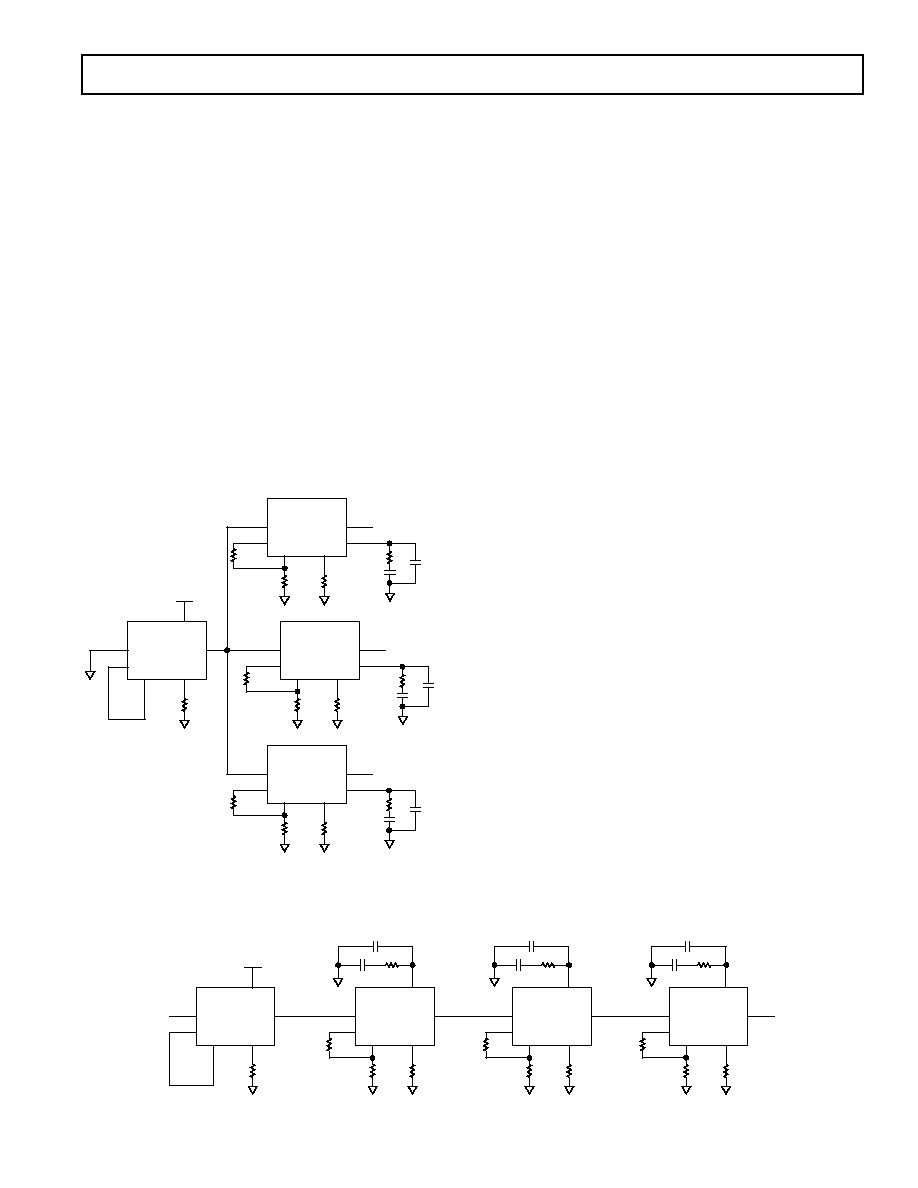
The phase adjusted output from the ADN8830 is available at
SYNCOUT (Pin 28). This pin can be used as a master clock
signal for driving other ADN8830 devices. Multiple ADN8830
devices can be either driven from a single master ADN8830
device by connecting its SYNCOUT pin to each slave's SYNCIN
pin or daisy-chained by connecting each device's SYNCOUT to
the next device's SYNCIN pin.
Phase shifting is useful in systems that use more than one
ADN8830 TEC controller. It ensures the ADN8830 devices
will not switch at the same time, which could create excessive
ripple on the power supply voltage. By adjusting the phase of
each device, the switching transients can be spaced equally over
the clock period, reducing potential supply ripple and easing the
instantaneous current demand from the supply.
Using a single master clock, each slave ADN8830 should have a
different value phase shift. For example, with four TEC con-
trollers, one slave device should be set for 90
∞ of phase shift,
another for 180
∞, and the last for 270∞. In a daisy-chain configu-
ration, each slave device would be set with equal phase. Using
the previous example, each slave would be set to 90
∞ with its
SYNCOUT pin connected to the next device's SYNCIN pin.
Examples are shown in Figures 7 and 8.
0.1 F
1k
1nF
24
1.5M
0.1 F
1k
1nF
24
ADN8830
SLAVE
25
29
26
28
100k
7
100k
NC
ADN8830
MASTER
25
29
26
R
FREQ
28
ADN8830
SLAVE
25
29
26
1.5M
0.1 F
1k
1nF
24
28
50k
7
150k
NC
ADN8830
SLAVE
25
29
26
28
150k
7
50k
NC
6
V
DD
24
Figure 7. Multiple ADN8830 Devices Driven from
a Master Clock
Soft Start on Power-Up
The ADN8830 can be programmed to ramp up for a specified
time after the power supply is applied or after shutdown is
de-asserted. This feature, known as soft start, is useful for
gradually increasing the duty cycle of the PWM amplifier. The
soft start time is set with a single capacitor connected from Pin 27
to ground according to Equation 14.
SS
SS
C
=
◊
150
(14)
where C
SS
is the value of the capacitor in microfarads, and
SS
is
the soft start time in milliseconds. To set a soft start time of 15 ms,
C
SS
should equal 0.1
µF. A minimum soft start time of 10 ms is
recommended to ensure proper initialization of the ADN8830
on power-up.
Shutdown Mode
The ADN8830 has a shutdown mode that deactivates the output
stage and puts the device into a low current standby state. The
current draw for the ADN8830 in shutdown is less than 100
µA.
The shutdown input, Pin 3, is active low. To shut down the
device, Pin 3 should be driven to logic low. Once a logic high is
applied, the ADN8830 will reactivate after the delay set by the
soft start circuitry. Refer to the Soft Start on Power-Up section
for more details on this feature.
Pin 3 should not be left floating as there are no internal pull-up
or pull-down resistors. If the shutdown function is not required,
Pin 3 should be tied to V
DD
to ensure the device is always active.
Compensation Loop
The ADN8830 TEC controller has a built-in amplifier dedicated
for loop compensation. The exact compensation network is set
by the user and can vary from a simple integrator to PI, PID, or
any other type of network. The type of compensation and com-
ponent values should be determined by the user since it will
depend on the thermal response of the object and the TEC. One
method for determining these values empirically is to input a step
function to TEMPSET, thus changing the target temperature,
and adjusting the compensation network to minimize the set-
tling time of the object's temperature.
A typical compensation network used for temperature control
of a laser module is a PID loop, which consists of a very low
frequency pole and two separate zeros at higher frequencies.
Figure 9 shows a simple network for implementing PID com-
pensation. An additional pole is added at a higher frequency
than the zeros to reduce the noise sensitivity of the control loop.
The bode plot of the magnitude is shown in Figure 10.
29
6
ADN8830
MASTER
25
NC
26
R
FREQ
ADN8830
SLAVE
25
29
26
1.5M
28
50k
7
150k
28
25
29
26
1.5M
28
50k
7
150k
25
29
26
1.5M
28
50k
7
150k
NC
V
DD
24
24
24
24
1k
0.1 F
1nF
1k
0.1 F
1nF
1k
0.1 F
1nF
ADN8830
SLAVE
ADN8830
SLAVE
Figure 8. Multiple ADN8830 Devices Using a Daisy Chain
REV. C
≠12≠
ADN8830
The unity-gain crossover frequency of the feedforward amplifier
is given as
f
R C
TEC GAIN
dB
0
1
2
3 1
80
=
◊
◊
(15)
To ensure stability, the unity-gain crossover frequency should be
lower than the thermal time constant of the TEC and thermistor.
However, this thermal time constant may not be specified and
can be difficult to characterize.
There are many texts written on loop stabilization, and it is beyond
the scope of this data sheet to discuss all methods and trade-offs
in optimizing compensation networks. A simple method that
can be used to empirically determine a PID compensation loop
as shown in Figure 9 involves the following procedure:
1. Connect thermistor and TEC to the ADN8830 application
circuit. Power does not need to be applied to the laser diode
for this procedure. Monitor output voltage across the TEC
with an oscilloscope.
2. Short C1 and open C2, leaving just R1 and R3 as a simple
proportional-only compensation loop.
3. While maintaining a constant TEMPSET voltage, increase
the ratio of R1/R3, thus increasing the gain until loop oscilla-
tion starts to occur. Decrease this ratio by a factor of 2 from
the point of oscillation. The R1/R3 ratio will likely be less
than unity for most laser modules.
4. Add C1 capacitor and decrease value until oscillation starts,
then increase by a factor of 2. A good initial starting value for
C1 is to create a unity-gain crossover of 0.1 Hz based on
Equation 15.
5. Short R2 and increase C2 until oscillation starts. At this point,
either C2 can be decreased or R2 can be added to regain
stability. Generally speaking, R2 will be greater than R3 and
C2 will be one or more orders of magnitude less than C1.
6. TEMPSET should be adjusted with a step change while
observing the output voltage settling time. A step change of
100 mV should suffice. From here, C2, R2, and even C1 can
be decreased to minimize settling time at the expense of
additional output voltage overshoot.
7. An additional feedback capacitor, CF, in parallel with R1
and C1, can be added to add another high frequency pole. In
many cases, this improves the stability of the system without
increasing the settling time as out-of-band noise is filtered
out of the control signal. A 330 pF to 1 nF capacitor should
suffice, if required.
The typical values shown in the typical application circuit in
Figure 1 have R1 = 100 k
, R2 = 1 M, R3 = 205 k, C1 = 10 µF,
C2 = 1
µF, and an additional feedback capacitor of 330 pF. For
most pump laser modules, this results in a 10
∞C TEMPSET step
settling time to within 0.1
∞C in less than 5 seconds.
ADN8830
12
COMPOUT
TEMPCTL
COMPFB
13
R3
R2
R1
C1
14
C2
REFERENCE
VOLTAGE
CF
Figure 9. Implementing a PID Compensation Loop
FREQUENCY (Hz LOG SCALE)
R1
R3
MA
GNITUDE (LOG SCALE)
R1
R2||R3
1
2 R1C1
1
2 C2(R2+R3)
1
2 R2C2
0dB
1
2 R3C1
Figure 10. Bode Plot for PID Compensation
Using the TEC Controller ADN8830 with a Wave Locker
Many optical applications require precision control of laser
wavelength. The wavelength of the laser diode can be adjusted
by changing its temperature, which is done through temperature
control of the TEC. Wavelength control can be done by feeding
a wave locker or etalon output back to the microprocessor and
using the microprocessor to calculate and reinstruct the TEC
controller with a new target temperature. However, this method
is computationally expensive and has time delays before the
adjustment is done. A faster responding and simpler method is
to feed the wave locker signal back to the TEC controller for
direct temperature control.
The ADN8830 is designed to be compatible with a wave locker
controller. Figure 11 shows the basic schematic. The TEMPCTL
output from ADN8830 is proportional to the object's actual
temperature. This voltage is fed to the wave locker controller.
Also fed to the wave locker controller are the photodiode out-
puts from the wave locker, as well as the laser diode power and
a digital signal indicating a functional laser diode, both of which
come from the CW controller. The output of the wave locker
controller is then connected to the input of the compensation
network. This allows the wave locker controller to adjust the
TEC temperature based on the current temperature of the
object, the current wavelength of the laser diode, and the target
wavelength. Once the target wavelength is reached, the wave
locker controller sends a signal to the microcontroller indicating
that the laser signal is good.
ADN8830
COMPOUT
14
COMPFB
13
COMPENSATION
NETWORK
TEMPCTL
12
TEMP IN
LOCKER
PD1
LOCKER
PD2
LASER DIODE
POWER
LASER DIODE
GOOD
FROM
LOCKER
FROM CW
CONTROLLER
WAVE LOCKER
GOOD
TO
MICRO-
PROCESSOR
TEC
CONTROL
Figure 11. Using the ADN8830 with a Wave Locker

REV. C
ADN8830
≠13≠
Using TEMPOUT to Measure Temperature
The TEMPOUT pin is a voltage that is proportional to the
difference between the target temperature and the measured
thermistor temperature. The full equation for the voltage at
TEMPOUT is
TEMPOUT
THERMIN
TEMPSET
=
+ ◊
(
)
1 5
3
.
≠
(16)
The voltage range of TEMPOUT is 0 V to 3.0 V and is inde-
pendent of power supply voltage.
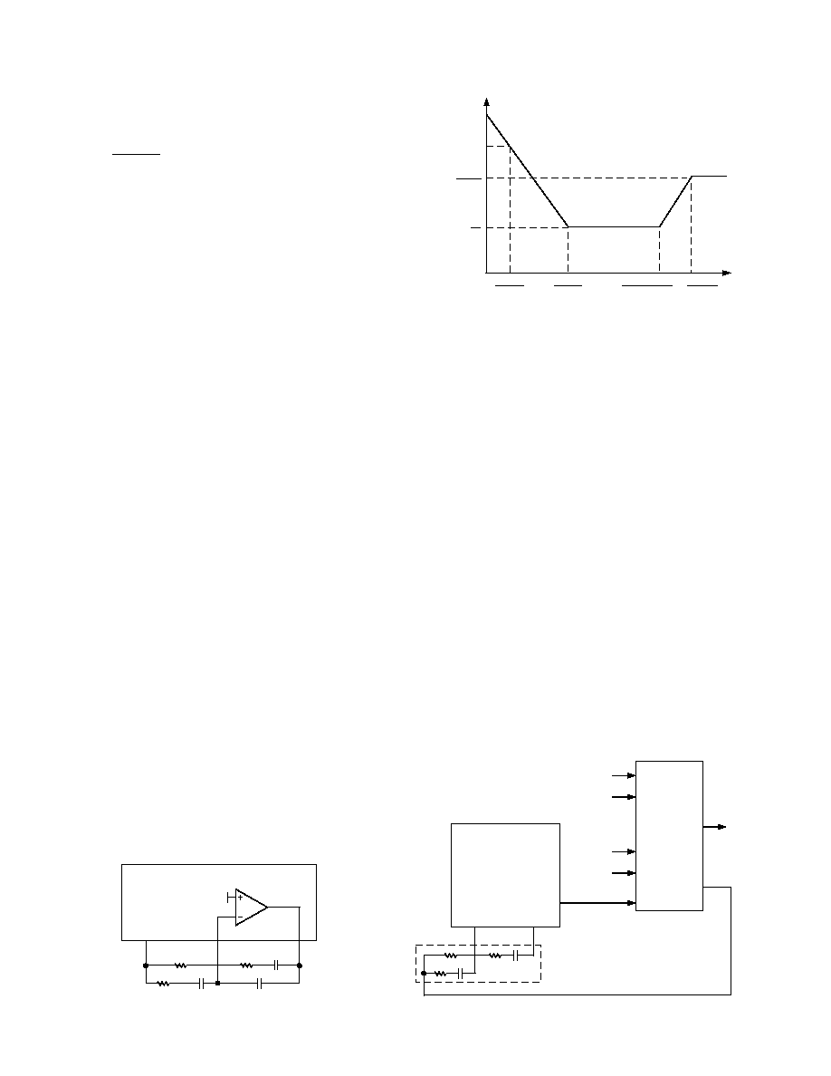
Setting the Maximum TEC Voltage and Current
The ADN8830 can be programmed for a maximum output volt-
age to protect the TEC. A voltage from 0 V to 1.5 V applied to
the VLIM (Pin 15) input to the ADN8830 sets the maximum
TEC voltage, V
TEC, MAX
. This voltage can be set with either a
resistor divider or from a DAC. Because the output of the
ADN8830 is bidirectional, this voltage sets both the upper
and lower limits of the TEC voltage. The equation governing
V
TEC, MAX
is given in Equation 17 and the graph of this equation
is shown in Figure 12.
V
V
VLIM
TEC MAX
,
.
≠
=
(
)
◊
1 5
4
(17)
VLIM (V)
5
0
0
2.0
0.5
V
TEC, MAX
(V)
1.0
1.5
4
3
2
1
Figure 12. VLIM Voltage vs. Maximum TEC Voltage
If the supply voltage is lower than V
TEC, MAX
, the maximum TEC
voltage will obviously be equal to the supply voltage. The voltage
to VLIM should not exceed 1.5 V since this causes improper
operation of the output voltage limiting circuitry. Setting VLIM to
1.5 V can be used to deactivate the TEC current without
shutting down the ADN8830 in the event of a system failure. If a
maximum TEC voltage is not required, VLIM should be con-
nected to ground. It is not advisable to leave VLIM floating as
this would cause unpredictable output behavior.
This feature should be used to limit the maximum output current
to the TEC as specified in the TEC data sheet. For example, if
the maximum TEC voltage is specified at 2 V, VLIM should be
set to 1 V. The maximum output voltage is then set to
±2 V.
Output Driver Amplifiers
The output voltage across the TEC as measured from Pin 19 to
Pin 9 can be monitored at Pin 16. This is labeled as VTEC in
the typical application schematic in Figure 1. The voltage at
VTEC can vary from 0 V to 3 V independent of the power
supply voltage. Its equation is given as
VTEC
V
V
OUT A
OUT B
=
◊
(
)
+
0 25
1 5
.
≠
.
(18)
where V
OUT A
and V
OUT B
are the voltages at Pins 19 and 9, respec-
tively. The ripple voltage at Pin 19 is filtered out internally and
does not appear at VTEC, leaving it as an accurate dc output of
the TEC voltage.
The TEC is driven with a differential voltage, allowing current
to flow in either direction through the TEC. This can provide
heat transfer either to or from the object being regulated without
the use of a negative voltage rail. The maximum output voltage
across the TEC is set by the voltage at VLIM (Pin 15). Refer to
the Setting the Maximum TEC Voltage and Current section for
details on this operation. With VLIM set to ground, the maximum
output voltage is the power supply voltage, V
DD
.
To achieve a differential output, the ADN8830 has two separate
output stages. OUT A is a switched output or pulse-width
modulated (PWM) amplifier, and OUT B is a high gain linear
amplifier. Although they achieve the same result, to provide
constant voltage and high current, their operation is different.
The exact equations for the two outputs are
OUT A
COMPOUT
OUT B
= ◊
(
)
+
4
1 5
≠ .
(19)
OUT B
COMPOUT
=
◊
(
)
+
≠
≠ .
.
14
1 5
1 5
(20)
where COMPOUT is the voltage at Pin 13. The voltage at
COMPOUT is determined by the compensation network that is
fed by the input amplifier, which receives its input voltage from
TEMPSET and THERMIN. Equation 20 is valid only in the
linear region of the linear amplifier. OUT B has a lower limit of
0 V and an upper limit of the power supply.
Because the COMPOUT voltage is not readily known, Equa-
tion 20 can be rewritten in terms of the TEC voltage, VTEC,
which is defined as OUT B ≠ OUT A.
OUT B
VTEC
= ◊
+
4
1 5
.
(21)
In Figure 1, Pins 10 and 11 provide the gate drive for Q3 and Q4,
which complete the linear output amplifier. This output voltage
is fed back to Pin 9 (OUT B) to close its loop. The gate-to-drain
capacitance of Q3 and Q4 provide the compensation for the
linear amplifier. If using the recommended FDW2520C transistors,
it will be necessary to add an additional 2.2 nF of capacitance
from the gate to the drain of the PMOS transistor to maintain
stability. A 3.3 nF capacitor should also be connected from the
drain to ground to prevent small oscillations when there is very
little or no current through the TEC.
These extra capacitors are specified only when using FDW2520C
transistors in the linear amplifier. If other transistors are used,
these values may need to be adjusted. To ensure the linear
amplifier is stable, the total gate-to-source capacitance for both
Q3 and Q4 should be at least 2.5 nF. Refer to the transistor's
data sheet for its typical gate-to-drain capacitance values.
The output of the linear amplifier is proportional to the voltage
at Pin 13 (COMPOUT). Because the linear amplifier operates
with a gain of 14, its output will typically be at either ground or
V
DD
if there is more than about 100 mA of current flowing
through the TEC. This ensures Q3 and Q4 will not be a domi-
nant source of power dissipation at high output currents.
REV. C
≠14≠
ADN8830
Inductor Selection
In addition to the external transistors, the PWM amplifier requires
an inductor and a capacitor at its output to filter the switched
output waveform. Proper inductor selection is important to
achieve the best efficiency. The duty cycle of the PWM sets the
OUT A output voltage and is
D
OUT A
V
DD
=
(22)
The average current through the inductor is equal to the TEC
current. The ripple current through the inductor, I
L
, varies
with the duty cycle and is equal to
I
V
D
D
L
f
L
DD
CLK
=
◊ ◊
(
)
◊
1 ≠
(23)
where f
CLK
is the clock frequency as set by the resistor R
FREQ
at
Pin 26 or an external clock frequency. Refer to the Setting the
Switching Frequency section for more information. Selecting a
faster switching frequency or a larger value inductor will reduce
the ripple current through the inductor. The waveform of the
inductor current is shown in Figure 13.
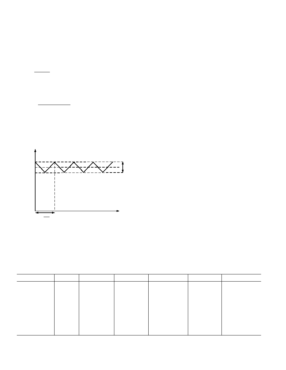
TIME
I
TEC
INDUCT
OR CURRENT (A)
I
L
1
f
CLK
T =
Figure 13. Current Waveform Through Inductor
It is important to select an inductor that can tolerate the maxi-
mum possible current that could pass through it. Most TECs
are specified with a maximum voltage and current for proper
and reliable operation. The maximum instantaneous inductor
current can be found as
I
I
I
L MAX
TEC MAX
L
,
,
.
=
+
◊
0 5
(24)
where I
L
can be found from Equation 23 with the appropriate
duty cycle calculated from Equation 22 with OUT A = V
TEC, MAX
.
Design Example 3
A TEC is specified with a maximum current of 1.5 A and maxi-
mum voltage of 2.5 V. The ADN8830 will be operating from a
3.3 V supply voltage with a 200 kHz clock and a 4.7
µH inductor.
The duty cycle of the PWM amplifier at 2.5 V is calculated to be
75.8%. Using Equation 23, the inductor ripple current is found
to be 664 mA. From Equation 24, the maximum inductor current
will be 1.82 A and should be considered when selecting the
inductor. Notice that increasing the clock frequency to 1 MHz would
reduce I
L, MAX
to 1.56 A.
Design Example 4
Using the same TEC as above, the ADN8830 will be powered
from 5.0 V instead. Here, the duty cycle is 50%, which happens
to be the worst-case duty cycle for inductor current ripple. Now
DIL equals 1.33 A with a 200 kHz clock, and I
L, MAX
is 2.83 A.
Reducing the inductor ripple current is another compelling
reason to operate the ADN8830 from a 3.3 V supply instead.
Table II lists some inductor manufacturers and part numbers
along with some key specifications. The column I
MAX
refers to the
maximum current at which the inductor is rated to remain linear.
Although higher currents can be pushed through the inductor,
efficiency and ripple voltage will be dramatically degraded.
This is by no means a complete list of manufacturers or inductors
that can be used in the application. More information on these
inductors is available at their websites. Note the trade-offs
between inductor height, maximum current, and series resistance.
Smaller inductors cannot handle as muËH current and therefore
require higher clock speeds to reduce their ripple current. They
also have higher series resistance, which can lower the overall
efficiency of the ADN8830.
PWM Output Filter Requirements
The switching of Q1 and Q2 creates a pulse width modulated
(PWM) square wave from 0 V to V
DD
. This square wave must
be filtered sufficiently to create a steady voltage that will drive
the TEC. The ripple voltage across the TEC is a function of the
inductor ripple current, the L-C filter cutoff frequency, and the
equivalent series resistance (ESR) of the filter capacitor. The
equivalent circuit for the PWM side is given in Figure 14.
Table II. Partial List of Inductors and Key Specifications
Inductance ( H)
I
MAX
(A)
R
S, TYP
(m )
Height (mm)
Part Number
Manufacturer
Website
4.7
1.1
200
1
LPO1704-472M
Coilcraft
www.coilcraft.com
4.7
1.59
55
2
A918CY-4R7M
Toko
www.toko.com
4.7
3.9
48
2.8
UP2.8B-4R7
Cooper
www.cooperet.com
4.7
1.5
90
3
DO1608C-472
Coilcraft
www.coilcraft.com
4.7
1.32
56
3
CDRH4D28 4R7
Sumida
www.sumida.com
4.7
7.5
12
4.5
892NAS-4R7M
Toko
www.toko.com
4.7
*
5.4
18
5.2
DO3316P-472
Coilcraft
www.coilcraft.com
10
2.7
80
2.8
UP2.8B-100
Cooper
www.cooperet.com
15
8
32
8
DO5022P-153HC
Coilcraft
www.coilcraft.com
47
4.5
86
7.1
DO5022P-473
Coilcraft
www.coilcraft.com
*Recommend inductor in typical application circuit Figure 1.
REV. C
ADN8830
≠15≠
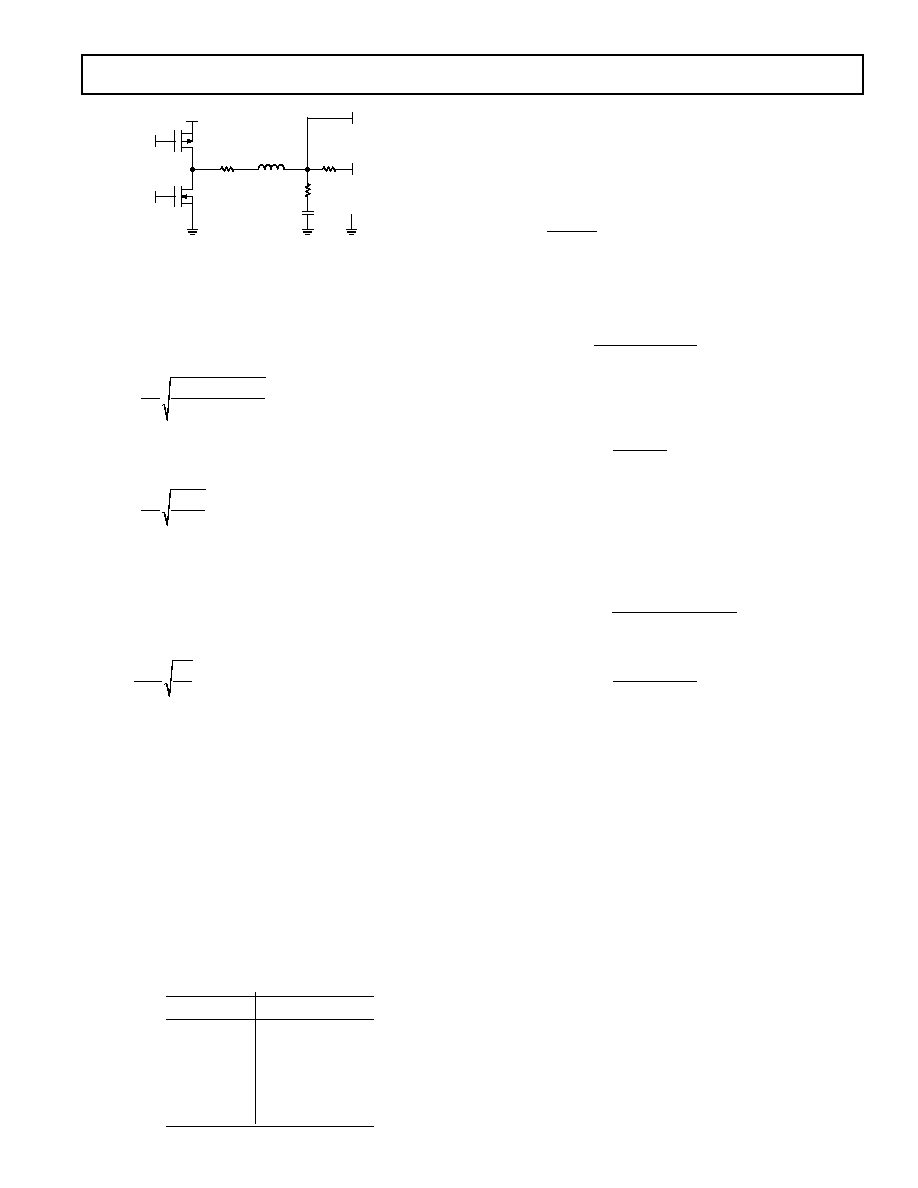
OUT B
C1
R1
R
L
L1
R2
PVDD
P1
Q1
N1
Q2
OUT A
V
X
DENOTES
PGND
Figure 14. Equivalent Circuit for PWM Amplifier and Filter
In this circuit, R
L
is the TEC resistance, R2 is the parasitic
resistance of the inductor combined with the equivalent r
DS, ON
of Q1 and Q2, and R1 is the ESR of C1. The voltage, V
X
, is the
pulse-width modulated waveform that switches between PVDD
and ground. This is a second-order low-pass filter with an exact
cutoff frequency of
f
R
R
R
R
C L
C
L
L
=
+
+
(
)
1
2
2
1
1 1
(25)
Practically speaking, R1 and R2 are several tens of milliohms and
are much smaller than the TEC resistance, which can be a few
ohms. The cutoff frequency can be roughly approximated as
f
C L
C
=
1
2
1
1 1
(26)
This cutoff frequency should be much lower than the clock
frequency to achieve adequate filtering of the switched output
waveform. Also of importance is the damping factor, , of the
L-C filter. Too low a damping factor will result in a longer
settling time and could potentially cause stability problems for
the temperature control loop. Neglecting R1 and R2 again, the
damping factor is simply
=
1
2
1
1
R
L
C
L
(27)
Using the recommended values of L1 = 4.7
µH and C1 = 22 µF
results in a cutoff frequency of 15.7 kHz. With a TEC resistance
of 2
, the damping factor is 0.12. The cutoff frequency can be
decreased to lower the output voltage ripple with slower clock
frequencies by increasing L1 or C1. Increasing C1 may appear
to be a simpler approach as it would not increase the physical
size of the inductor, but there is a potential stability danger in
lowering the damping factor too far. It is recommended that
remain greater than 0.05 to provide a reasonable settling time
for the TEC. Increasing
also makes finding the proper PID
compensation easier as there is less ringing in the L-C output
filter. To allow adequate phase and gain margin for the PWM
amplifier, Table III should be used to find the lower limit of
cutoff frequency for a given damping factor.
Table III. Minimum L-C Filter Cutoff
Frequency vs. Damping Factor
f
C, MIN
(kHz)
0.05
8
0.1
4
0.2
2
0.3
1.9
0.5
1.6
> 0.707
1.5
Calculating PWM Output Ripple Voltage
Although it may seem that f
C
can be arbitrarily lowered to reduce
output ripple, the ripple voltage is also dependent on the ESR of
C1, shown as R1 in Figure 14. This resistance creates a zero
that turns the second-order filter into a first-order filter at high
frequencies. The location of this zero is
Z
R C
1
1
2
1 1
=
(28)
With a clock frequency greater than Z1, and presumably greater
than f
C
, the output voltage ripple is
OUT A
I
R
L
=
◊ 1
(29)
OUT A
V
D
D R
L f
for f
Z
DD
CLK
CLK
=
(
)
>
(
)
1
1
1
1
≠
(30)
The worst-case voltage ripple occurs when the duty cycle of the
PWM output is exactly 50%, or when OUT A = 0.5 V
DD
. As
shown in Equation 31
OUT A
V
R
f
L
for f
Z
MAX
DD
CLK
CLK
>
(
)
1
4
1
1
(31)
Here it can be directly seen that increasing the inductor value or
clock frequency will reduce the ripple. Choosing a low ESR
capacitor will ensure R1 remains low. Operating from a lower
supply voltage will also help reduce the output ripple voltage
from the L-C filter. With a clock frequency equal to Z1 but
presumably greater than f
C
, the worst-case output voltage ripple is
OUT A
V
R C
f
L C f
for f
Z
MAX
DD
CLK
CLK
CLK
=
+
(
)
=
(
)
16 1
1
1
32 1 1
1
2
2
2
(32)
Which, if f
CLK
< Z1, can be further simplified to
OUT A
V
L C f
for f
Z
MAX
DD
CLK
CLK
=
<
(
)
32 1 1
1
2
(33)
A typical 100
µF surface-mount electrolytic capacitor can have
an ESR of over 100 m
, pulling this zero to below 16 kHz, and
resulting in an excess of ripple voltage across the TEC. Low ESR
capacitors, such as ceramic or polymer aluminum capacitors,
are recommended instead. Polymer aluminum capacitors can
provide more bulk capacitance per unit area over ceramic ones,
saving board space. Table IV shows a limited list of capacitors
with their equivalent series resistances.
This is by no means a complete list of all capacitor manufacturers
or capacitor types that can be used in the application. The 22
µF
capacitor recommended has a maximum ESR of 35 m
, which
puts Z1 at 207 kHz. Using a 3.3 V supply with the recommended
inductor and capacitor listed with a 1 MHz clock frequency will
yield a worst-case ripple voltage at OUT A of about 6 mV.
External FET Requirements
External FETs are required for both the PWM and linear amplifiers
that drive OUT A and OUT B from the ADN8830. Although it
is important to select FETs that can supply the maximum current
required to the TEC, they should also have a low enough resis-
tance (r
DS, ON
) to prevent excessive power dissipation and improve
efficiency. Other key requirements from these FET pairs are
slightly different for the PWM and linear outputs.

REV. C
≠16≠
ADN8830
The gate drive outputs for the PWM amplifier at P1 (Pin 21)
and N1 (Pin 22) have a typical nonoverlap delay of 65 ns.
This is done to ensure that one FET is completely off before
the other FET is turned on, preventing current from shooting
through both simultaneously.
The input capacitance (C
ISS
) of the FET should not exceed 5 nF.
The P1 and N1 outputs from the ADN8830 have a typical output
impedance of 6
. This creates a time constant in combination
with C
ISS
of the external FETs equal to 6
C
ISS
. To ensure
shoot-through does not occur through these FETs, this time
constant should remain less than 30 ns.
The linear output from the ADN8830 uses N2 (Pin 10) and
P2 (Pin 11) to drive the gates of the linear side FETs, shown as
Q3 and Q4 in Figure 1. Local compensation for the linear ampli-
fier is achieved through the gate-to-drain capacitances (C
GD
) of
Q3 and Q4. The value of C
GD
, which can be determined from
the data sheet, is usually referred to as C
RSS
, the reverse transfer
capacitance. The exact C
RSS
value should be determined from a
graph that shows capacitance versus drain-to-source voltage,
using the power supply voltage as the appropriate V
DS
.
To ensure stability of the linear amplifier, the total C
GD
of the
PMOS device, Q3, should be greater than 2.5 nF and the total
C
GD
of the NMOS should be greater than 150 pF. External
capacitance can be added around the FET to increase the effective
C
GD
of the transistor. This is the function of C6 in the typical
application schematic shown in Figure 1. If external capacitance
must be added, it will generally only be required around the
PMOS transistor.
In the event of zero output current through the TEC, there will
be no current flowing through Q3 and Q4. In this condition,
these FETs will not provide any small signal gain and thus no
negative feedback for the linear amplifier. This leaves only a
feedforward signal path through C
GD
, which could cause a
settling problem at OUT B. This is often seen as a small signal
oscillation at OUT B, but only when the TEC is at or very near
zero current.
The remedy for this potential minor instability is to add
capacitance from OUT B to ground. This may need to be deter-
mined empirically, but a good starting point is 1.5 times the
total C
GD
. This is the function of C12 in Figure 1. Note that
while adding more C
GD
around Q3 and Q4 will help to ensure
stability, it could potentially increase instability in the zero current
dead band region, requiring additional capacitance from
OUT B to ground.
Bear in mind that the addition of these capacitors is only
for local stabilization. The stability of the entire TEC appli-
cation may need adjustment, which should be done around the
compensation amplifier. This is covered in the Compensation
Loop section.
There is one additional consideration for selecting both the
linear output FETs; they must have a minimum threshold
voltage (V
T
) of 0.6 V. Lower threshold voltages could cause
shoot-through current in the linear output transistors.
Table V shows the recommended FETs that can be used for the
linear output in the ADN8830 application. Table V includes the
appropriate external gate-to-drain capacitance (external C
GD
)
and snubber capacitor value (C
SNUB
) connected from OUT B to
ground that should be added to ensure local stability. Table VI
shows the recommended PWM output FETs. Although other
transistors can be used, these combinations have been tested
and are proved stable and reliable for typical applications.
Data sheets for these devices can be found at their respective
websites:
Fairchild ≠ www.fairchildsemi.com
Vishay Siliconix ≠ www.vishay.com
International Rectifier ≠ www.irf.com
Calculating Power Dissipation and Efficiency
The total efficiency of the ADN8830 application circuit is simply
the ratio of the output power to the TEC divided by the total
power delivered from the supply. The idea in minimizing power
dissipation is to avoid both drawing additional power and reduc-
ing heat generated from the circuit. The dominant sources
of power dissipation will include resistive losses, gate charge
loss, core loss from the inductor, and the current used by the
ADN8830 itself.
The on-channel resistance of both the linear and PWM output
FETs will affect efficiency primarily at high output currents.
Because the linear amplifier operates in a high gain configuration,
it will be at either ground or V
DD
when significant current is
flowing through the TEC. In this condition, the power dissipation
through the linear output FET will be
P
r
I
FET LIN
DS ON
TEC
,
,
=
◊
2
(34)
using either the r
DS, ON
for the NMOS or the PMOS depending
on the direction of the current flow. In the typical application
setup in Figure 2, if the TEC is cooling the target object, the
PMOS is sourcing the current. If the TEC is heating the
object, the NMOS will be sinking current.
Table IV. Partial List of Capacitors and Key Specifications
Value ( F)
ESR (m )
Voltage Rating (V)
Part Number
Manufacturer
Website
10
60
6.3
NSP100M6.3D2TR
NIC Components
www.niccomp.com
22
*
35
8
ESRD220M08B
Cornell Dubilier
www.cornell-dubilier.com
22
35
8
NSP220M8D5TR
NIC Components
www.niccomp.com
22
35
8
EEFFD0K220R
Panasonic
www.maco.panasonic.co.jp
47
25
6.3
NSP470M6.3D2TR
NIC Components
www.niccomp.com
68
18
8
ESRD680M08B
Cornell Dubilier
www.cornell-dubilier.com
100
95
10
594D107X_010C2T
Vishay
www.vishay.com
*Recommend capacitor in typical application circuit Figure 1.
REV. C
ADN8830
≠17≠
Although the FETs that drive OUT A alternate between Q1 and
Q2 being on, they have an equivalent series resistance that is
equal to a weighted average of their r
DS, ON
values.
R
D
r
D
r
EQIV
DS P
DS N
= ◊
+
(
)
◊
,
,
≠
1
1
1
(35)
The resistive power loss from the PWM transistors is then
P
R
I
FET PWM
EQIV
TEC
,
=
◊
2
(36)
There is also a power loss from the continuing charging and
discharging of the gate capacitances on Q1 and Q2. The power
dissipated due to gate charge loss (P
GCL
) is
P
C
V
f
GCL
ISS
DD
CLK
=
1
2
2
(37)
using the appropriate input capacitance (C
ISS
) for the NMOS
and PMOS. Both transistors are switching, so P
GCL
should be
calculated for each one and will be added to find the total power
dissipated from the circuit.
The series resistance of the inductor, R2 from Figure 14, will
also exhibit a power dissipation equal to
P
R
I
R
TEC
2
2
2
=
◊
(38)
Core loss from the inductor arises as a result of nonidealities of
the inductor. Although this is difficult to calculate explicitly, it
can be estimated as 80% of P
RLS
at 1 MHz switching frequen-
cies and 50% of P
RL
at 100 kHz. Judging conservatively
P
P
LOSS
RL
=
◊
0 8
.
(39)
Finally, the power dissipated by the ADN8830 is equal to the
current used by the device multiplied by the supply voltage.
Again, this exact equation is difficult to determine as we have
already taken into account some of the current while finding the
gate charge loss. A reasonable estimate is to use 40 mA as the
total current used by the ADN8830. The power dissipated from
the device itself is
P
V
mA
ADN
DD
8830
10
=
◊
(40)
There are certainly other minor mechanisms for power dissipa-
tion in the circuit. However, a rough estimate of the total power
dissipated can be found by summing the preceding power dissi-
pation equations. Efficiency is then found by comparing the
power dissipated with the required output power to the load.
Efficiency
P
P
P
LOAD
LOAD
DISS TOT
=
+
,
(41)
where
P
I
V
LOAD
LOAD
LOAD
=
◊
The measured efficiency of the system will likely be less than the
calculated efficiency. Measuring the efficiency of the application
circuit is fairly simple but must be done in an exact manner to
ensure the correct numbers are being measured. Using two high
current, low impedance ammeters and two voltmeters, the cir-
cuit should be set up as shown in Figure 15.
A
V
DD
POWER SUPPLY
GND
ADN8830
V
V
A
TEC
LOAD
Figure 15. Measuring Efficiency of the ADN8830 Circuit
Table V. Recommended FETs for Linear Output Amplifier
Part Number
Type
C
GD
(nF)
Ext. C
GD
(nF)
C
SNUB
(nF)
r
DS, ON
(m )
I
MAX
(A)
Manufacturer
FDW2520C
*
NMOS
0.17
18
6.0
Fairchild
PMOS
0.15
2.2
3.3
35
4.5
Fairchild
IRF7401
NMOS
0.5
22
8.7
International Rectifier
IRF7233
PMOS
2.2
1.0
3.3
20
9.5
International Rectifier
FDR6674A
NMOS
0.23
9.5
11.5
Fairchild
FDR840P
PMOS
0.6
1.0
3.3
12
10
Fairchild
*Recommend transistors in typical application circuit Figure 1.
Table VI. Recommended FETs for PWM Output Amplifier
Part Number
Type
C
ISS
(nF)
r
DS,ON
(m )
Continuous I
MAX
(A)
Manufacturer
FDW2520C
*
NMOS
1.33
18
6.0
Fairchild
PMOS
1.33
35
4.5
Fairchild
Si7904DN
NMOS
1.0
30
5.3
Vishay Siliconix
Si7401DN
PMOS
3.5
17
7.3
Vishay Siliconix
IRF7401
NMOS
1.6
22
8.7
International Rectifier
IRF7404
PMOS
1.5
40
6.7
International Rectifier
*Recommend transistors in typical application circuit Figure 1.
REV. C
≠18≠
ADN8830
The voltmeter to the TEC or output load should include the series
ammeter since the power delivered to the ammeter is considered part
of the total output power. However, the voltmeter measuring the
voltage delivered to the ADN8830 circuit should not include the
series ammeter from the power supply. This prevents a false supply
voltage power measurement since we are interested only in the
supply voltage power delivered to the ADN8830 circuit. Figures 16
and 17 show some efficiency measurements using the typical appli-
cation circuit shown in Figure 1.
I
TEC
(mA)
100
80
0
0
2,000
500
EFFICIENCY (%)
1,000
1,500
60
40
20
V
SY
= 5V
V
SY
= 3V
Figure 16. Efficiency with f
CLK
= 1 MHz
I
TEC
(mA)
100
80
0
0
2,000
500
EFFICIENCY (%)
1,000
1,500
60
40
20
V
SY
= 5V
V
SY
= 3V
Figure 17. Efficiency with f
CLK
= 200 kHz
Note that higher efficiency can be achieved using a lower supply
voltage or a slower clock frequency. This is due to the fact that the
dominant source of power dissipation at high clock frequencies is the
gate charge loss on the PWM transistors.
Layout Considerations
The two key considerations for laying out the board for the
ADN8830 are to minimize both the series resistance in the output
and the potential noise pickup in the precision input section. The
best way to accomplish both of these objectives is to divide the
layout into two sections, one for the output components and the
other for the remainder of the circuit. These sections should have
independent power supply and ground current paths that are each
connected together at a single point near the power supply. This is
used to minimize power supply and ground voltage bounce on the
more sensitive input stages to the ADN8830 caused by the switch-
ing of the PWM output. Such a layout technique is referred to as a
"star" ground and supply connection. Figure 18 shows a block dia-
gram of the concept.
V
DD
POWER SUPPLY
GND
TEC
OR
LOAD
OUTPUT
SECTION
NOISE
SENSITIVE
SECTION
PGND
PVDD
AGND
AVDD
Figure 18. Using Star Connections to Minimize
Noise Pickup from Switched Output
The low noise power and ground are referred to as AVDD and
AGND, with the output supply and ground paths labeled PVDD
and PGND. These pins are labeled on the ADN8830 and should
be connected appropriately. Both sets of external FETs should be
connected to PVDD and PGND. All output filtering and PVDD
supply bypass capacitors should be connected to PGND.
All remaining connections to ground and power supply should be
done through AVDD and AGND. A 4-layer board layout is rec-
ommended for best performance with split power and ground
planes between the top and bottom layers. This provides the
lowest impedance for both supply and ground points. Setting the
ADN8830 above the AGND plane will reduce the potential noise
injection into the device. Figure 19 shows the top layer of the
layout used for the ADN8830 evaluation boards, highlighting the
power and ground split planes.
Figure 19. Top Layer Reference Layout for ADN8830
Proper supply voltage bypassing should also be taken into consid-
eration to minimize the ripple voltage on the power supply. A
minimum bypass capacitance of 10
µF should be placed in close
proximity to each component connected to the power supply. This
includes Pins 8 and 20 on the ADN8830 and both external PMOS
transistors. An additional 0.1
µF capacitor should be placed in
parallel to each 10
µF capacitor to provide bypass for high fre-
quency noise. Using a large bulk capacitor, 100
µF or greater, in
parallel with a low ESR capacitor where AVDD and PVDD con-
nect will further improve voltage supply ripple. This is covered in
more detail in the Power Supply Ripple section.
REV. C
ADN8830
≠19≠
Power Supply Ripple
Minimizing ripple on the power supply voltage can be an impor-
tant consideration, particularly in signal source laser applications.
If the laser diode is operated from the same supply rail as the TEC
controller, ripple on the supply voltage could cause inadvertent
modulation of the laser frequency. As most laser diodes are driven
from a 5 V supply, it is recommended the ADN8830 be operated
from a separate 3.3 V regulated supply unless higher TEC voltages
are required. Operation from 3.3 V also improves efficiency, thus
minimizing power dissipation.
The power supply ripple is primarily a function of the supply by-
pass capacitance, also called bulk capacitance, and the inductor
ripple current. Similar to the L-C filter at the PWM amplifier
output, using more capacitance with low equivalent series resis-
tance (ESR) will lower the supply ripple. A larger inductor value
will reduce the inductor ripple current, but this may not be
practical in the application. A recommended approach is to use a
standard electrolytic capacitor in parallel with a low ESR capacitor.
A surface-mount 220
µF electrolytic in parallel with a 22 µF poly-
mer aluminum low ESR capacitor can occupy an approximate total
board area of only 0.94 square inches or 61 square millimeters.
Using these capacitors along with a 4.7
µH inductor can yield a
supply ripple of less than 5 mV.
High frequency transient spikes may appear on the supply voltage
as well. This is due to the fast switching times on the PWM transis-
tors and the sharp edges of their gate voltages. Although these
transient spikes can reach several tens of millivolts at their peak,
they typically last for less than 20 ns and have a resonance greater
than 100 MHz. Additional bulk capacitance will not appreciably
affect the level of these spikes as such capacitance is not reactive at
these frequencies. Adding 0.01
µF ceramic capacitors on the sup-
ply line near the PWM PMOS transistor can reduce this switching
noise. Inserting an RF inductor with a High-Q around 100 MHz in
series with PVDD will also block this noise from traveling back to
the power supply.
Setting Maximum Output Current and Short-Circuit
Protection
Although the maximum output voltage can be programmed
through VLIM to protect the TEC from overvoltage damage,
the user may wish to protect the ADN8830 circuit from a possible
short circuit at the output. Such a short could quickly damage the
external FETs or even the power supply since they would attempt
to drive excessive current. Figure 20 shows a simple modification
that will protect the system from an output short circuit.
SD
C1
1 F
R2
1k
DENOTES
PGND
R1
1M
D1
MA116CT-ND
OR
EQUIVALENT
AVDD
Q1
FDV304P
OR EQUIVALENT
PVDD
R
S
10m
R4
100k
R3
1k
PVDD
DENOTES
AGND
TO
FETS
AND
DECOUPLING
CAPS
V
S
V
X
AD8601
Figure 20. Implementing Output Short-Circuit Protection
A 10 m
resistor placed in series with the PVDD supply line creates a
voltage drop proportional to the absolute value of the output current.
The AD8601 is a CMOS amplifier that is configured as a com-
parator. As long as the voltage at its inverting input (V
S
) exceeds
the voltage set by the resistor divider at the noninverting input (V
X
),
the gate of Q1 will remain at ground. This leaves Q1 on, effectively
connecting D1 to the positive rail and leaving the voltage on C1 at
V
DD
. Should enough current flow through R
S
to drop V
S
below V
X
,
Q1 will turn off and C1 will discharge through R2 down to a logic
low to activate the ADN8830 shutdown. Once V
S
returns to a
voltage greater than V
X
, Q1 will turn back on and C1 will charge
back to V
DD
through R1. The shutdown and reactivation time
constants are approximately
SD
ON
C
R
C
R
=
◊
=
◊
1
1
1
1
(42)
The shutdown time constant should be a minimum of 10 clock
cycles to ensure high current switching transients do not trigger a
false activation. If powered from 5 V, the circuit shown will shut
down the ADN8830 should PVDD deliver over 5 A for more than
1 ms. After shutdown, the circuit will reactivate the ADN8830 in
about 1 second.
The voltage drop across R
S
is found as
V
I
R R
V
R
OUT
L
S
DD
S
=
2
(43)
where R
L
is the load resistance or resistance of the TEC and is
the efficiency of the system. An estimate of efficiency can be calculated
either from the Calculating Power Dissipation and Efficiency section
or from Figures 16 and 17. A reasonable approximation is =
0.85. Although the exact resistance of a TEC varies with tempera-
ture, an estimation can be made by dividing the maximum voltage
rating of the TEC by its maximum current rating.
In addition to providing protection against a short at the output,
this circuit will also protect the FETs against shoot-through current.
Shoot-through will not occur when using the recommended
transistors and additional capacitance shown in Tables V and VI.
However, if different transistors are used where their shoot-
through potential is unknown, implementing the short-circuit
protection circuit will unconditionally protect these transistors.
To set a maximum output current limit, use the circuit in Figure
21. This circuit can share the 10 m
power supply shunt resistor
as the short-circuit protection circuit to sense the output current.
In normal operation Q1 is on, pulling the ADN8830 VLIM pin
down to the voltage set by VLIMIT. This sets the maximum out-
put voltage limit as described in the Setting the Maximum TEC
Voltage and Current section.
TO
VLIM
R2
1.47k
DENOTES
PGND
AVDD
Q1
FDV301N
OR
EQUIVALENT
PVDD
R
S
10m
R4
100k
R3
178
PVDD
DENOTES
AGND
V
SY
V
X
AD8605
VLIMIT
(0V TO 1.5V)
R1
3.48k
C1
1nF
TO
FETS
AND
DECOUPLING
CAPS
Figure 21. Setting a Maximum Output Current Limit
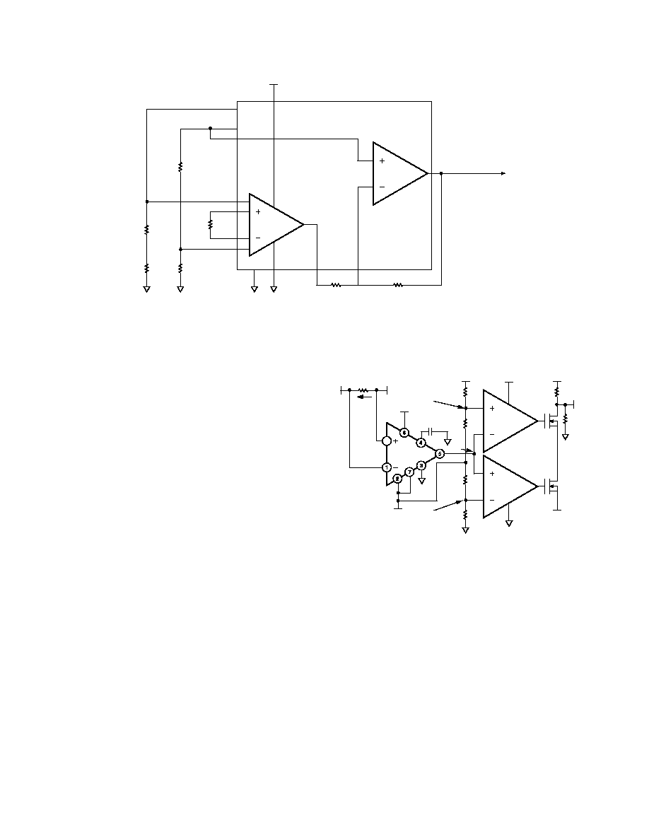
REV. C
≠20≠
ADN8830
If the voltage at V
SY
drops below V
X
, Q1 is turned off and the
VLIM pin will be set to 1.5 V, effectively setting the maximum
voltage across the outputs to 0 V. The voltage divider for V
X
is
calculated from Equation 43.
Design Example 5
A maximum output current limit needs to be set at 1.5 A for a
TEC with a maximum voltage rating of 2.5 V. The ADN8830 is
powered from 5 V. The TEC resistance is estimated at 1.67
and
efficiency at 85%. Using Equation 43, the voltage drop across
R
S
will be 8.8 mV when 1.5 A is delivered to the TEC. The trip
voltage V
X
is set to 4.991 V with R3 = 178
and R4 = 100 k
as shown in Figure 21. To set the output voltage limit to 2.5 V,
the voltage at VLIMIT should be set to 0.875 V according to
Equation 17.
The C1 capacitor is added to smooth the voltage transitions at
VLIM. Once an overcurrent condition is detected, the output
voltage will turn down to 0 V within 30 ms.
For a more exact measurement of the output current, place a
sense resistor in series with the output load, as shown in Figure 23.
The AD626 instrumentation amplifier is set for a gain of 100
with a reference voltage of 2.47 V from VREF. The output of
the AD626 is equal to 100
◊ R
S
◊ I
L
and is fed to the AD8602,
which is set up as a window comparator. With V
X
greater than
VLO but less than VHI, VLIM will be pulled down to the volt-
age at VLIMIT. Should V
X
fall outside the voltage window,
VLIM will be pulled to 1.5 V as in Figure 21. The trip points
should be set according to
VHI
VREF
R I
VLO
VREF
R I
S LIMIT
S LIMIT
=
+
◊
=
◊
+
100
100
≠
≠
(44)
AVDD
Q1,Q2
FDG6303N
OR
EQUIVA-
LENT
8
TO
VREF
1nF
AVDD
TO
OUT B
R
S
10m
I
L
TO
TEC
VLIMIT
(0V TO 1.5V)
TO
VLIM
R2
1.47k
R1
3.48k
AVDD
200k
300k
300k
200k
V
X
V
LO
AD8602
AD626
AVDD
V
HI
Figure 23. High Accuracy Output Current Limit
The upper and lower trip point voltages can be set independently,
allowing different maximum output current limits depending on
the direction of the current. The resistor divider for VHI and
VLO is tapped to VREF to maintain window accuracy with any
changes in VREF. Using the values from Figure 23 with a 5 V
supply, the output current will not exceed 1.5 A in either direction.
Adding the current sensing resistor will slightly reduce efficiency.
The power dissipated by this resistor is D
◊ ITEC2 ◊ R
S
if the
TEC is heating, or (1≠D)
◊ ITEC2 ◊ R
S
if the TEC is cooling.
Include this when calculating efficiency as described in the
Calculating Power Dissipation and Efficiency section.
25mV/ C
OUT
OA
ADT70
1k
OUT
IA
≠IN
OA
5.11k
AGND
4.99k
RGA
RGB
INST
AMP
≠IN
IA
+IN
IA
+IN
OA
R3
1k
R3
82.5
I
OUTB
I
OUTA
RTD
1k
R3
82.5
GND
SENSE
5V
NOTE: ADDITIONAL PINS OMITTED FOR CLARITY
TO THERM_IN
= 1V @ 25 C
Figure 22. Using an RTD for Temperature Feedback to the ADN8830
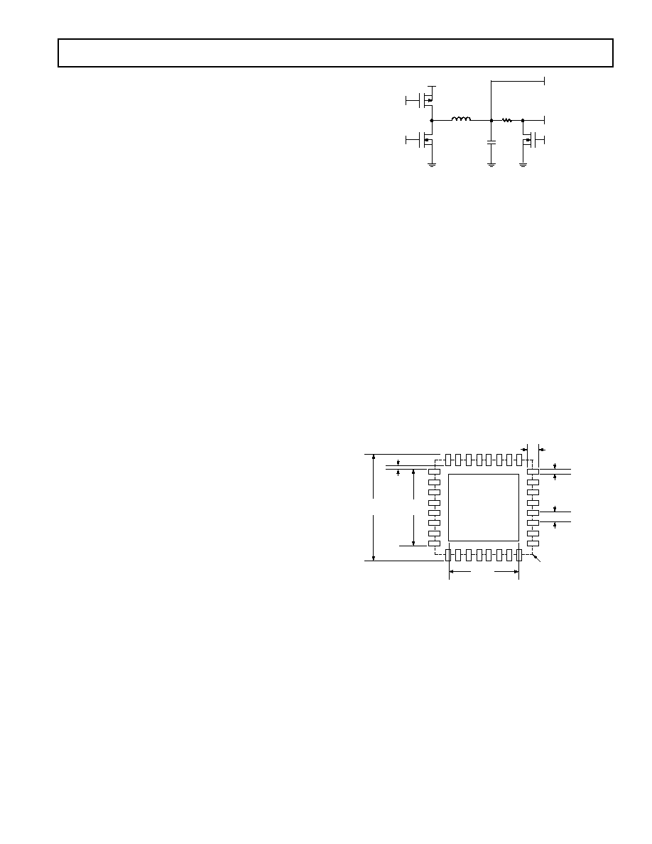
REV. C
ADN8830
≠21≠
Using an RTD for Temperature Sensing
The ADN8830 can be used with a resistive temperature device
(RTD) as the temperature feedback sensor. The resistance of an
RTD is linear with respect to temperature, offering an advan-
tage over thermistors that have an exponential relationship to
temperature. A constant current applied through an RTD will
yield a voltage proportional to temperature. However, this volt-
age could be on the order of only 0.5 mV/
∞C, thus requiring the
use of additional amplification to achieve a usable signal level.
The ADT70 from Analog Devices can be used to bias and amplify
the voltage across an RTD, which can then be fed directly to the
THERMIN pin on the ADN8830 to provide temperature
feedback for the TEC controller. The ADT70 uses a 0.9 mA
current source to drive the RTD and an instrumentation ampli-
fier with adjustable gain to boost the RTD voltage. Application
notes and typical schematics for this device can be found in the
ADT70 Data Sheet.
Most RTDs have a positive temperature coefficient, also called
tempco, as opposed to thermistors, which have a negative tempco.
For the OUT A output to drive the TEC≠ input as shown in
Figure 1, the signal from an RTD must be conditioned to create
a negative tempco. This can be easily done using an inverting
amplifier. Alternately, OUT A can be connected to drive TEC+
with OUT B driving TEC≠ with a positive tempco at THERMIN.
This is highlighted in the Output Driver Amplifiers section.
For the ADN8830, proper operation care should be taken
to ensure the voltage at THERMIN remains within 0.4 V
and 2.0 V. Using a 1 k
RTD with the ADT70 will yield a
THERMIN voltage of 0.9 V at 25
∞C. Using the application
circuit shown in Figure 22 will provide a nominal output
voltage of 1.0 V at 25
∞C and a total gain of 66.7 mV/.
Using an RTD with a temperature coefficient of 0.375
/∞C
will give a THERMIN voltage swing from 1.5 V at 5
∞C to
0.5 V at 45
∞C, well within the input range of the ADN8830.
Using a Resistive Load as a Heating Element
The ADN8830 can be used in applications that do not neces-
sarily drive a TEC but require only a high current output into a
load resistance. Such applications generally only require heating
above ambient temperature and simply use the power dissipated
by the load element to accomplish this. Because the power
dissipated by such an element is proportional to the square of
the output voltage, the ADN8830 application circuit must be
modified. Figure 24 shows the preferred method for driving a
heating element load.
OUT B
C1
R
L
L1
PVDD
P1
Q1
N1
Q2
N2
Q3
OUT A
NO CONNECTION TO P2 REQUIRED
Figure 24. Using the ADN8830 to Drive a Heating Element
Current is delivered from the PWM amplifier through Q3 when
the voltage at THERMIN is lower than TEMPSET. If the object
temperature is greater than the target temperature, Q3 will turn
off and the current through the load goes to zero, allowing the
object to cool back toward the ambient temperature. As the
target temperature is approached, a steady output current should
be reached. Naturally, a proper compensation network must be
found to ensure stability and adequate temperature settling time.
The P2 output from the ADN8830 should be left unconnected.
Suggested Pad Layout for CP-32 Package
Figure 25 shows the dimensions for the PC board pad layout for
the ADN8830, which is a 5 5, 32-lead lead frame chipscale
package. This package has a metallic heat slug that should be
soldered to a copper pad on the PC board. Although the pack-
age slug is electrically connected to the substrate of the IC, the
copper pad should be left electrically floating. This prevents
potential noise injection into the substrate while maintaining
good thermal conduction to the PC board.
0.10
(0.0039)
3.78
(0.1488)
5.36
(0.2110)
3.68
(0.1449)
0.28
(0.0110)
0.50
(0.0197)
0.69
(0.0272)
CONTROLLING DIMENSIONS ARE IN MILLIMETERS; INCH DIMENSIONS
(IN PARENTHESES) ARE ROUNDED-OFF MILLIMETER EQUIVALENTS FOR
REFERENCE ONLY AND ARE NOT APPROPRIATE FOR USE IN DESIGN
THERMAL PAD SHOULD BE SOLDERED TO AN ELECTRICALLY FLOATING
PAD ON THE PC BOARD
PACKAGE
OUTLINE
Figure 25. Suggested PC Board Layout for CP-32
Pad Landing
REV. C
≠22≠
ADN8830
OUTLINE DIMENSIONS
32-Lead Lead Frame Chip Scale Package [LFCSP]
(CP-32-1)
Dimensions shown in millimeters
COMPLIANT TO JEDEC STANDARDS MO-220-VHHD-2
0.30
0.23
0.18
0.20 REF
0.80 MAX
0.65 TYP
0.05 MAX
0.02 NOM
12
MAX
1.00
0.85
0.80
SEATING
PLANE
COPLANARITY
0.08
1
32
8
9
25
24
16
17
BOTTOM
VIEW
0.50
0.40
0.30
3.50 REF
0.50
BSC
PIN 1
INDICATOR
TOP
VIEW
5.00
BSC SQ
4.75
BSC SQ
SQ
3.25
3.10
2.95
PIN 1
INDICATOR
0.60 MAX
0.60 MAX
0.25 MIN

REV. C
ADN8830
≠23≠
Revision History
Location
Page
11/03--Data Sheet Changed from REV. B to REV. C.
Changes to ORDERING GUIDE . . . . . . . . . . . . . . . . . . . . . . . . . . . . . . . . . . . . . . . . . . . . . . . . . . . . . . . . . . . . . . . . . . . . . . . . . . . 3
Deleted Figure 24 . . . . . . . . . . . . . . . . . . . . . . . . . . . . . . . . . . . . . . . . . . . . . . . . . . . . . . . . . . . . . . . . . . . . . . . . . . . . . . . . . . . . . . 21
Deleted Boosting the Output Voltage section . . . . . . . . . . . . . . . . . . . . . . . . . . . . . . . . . . . . . . . . . . . . . . . . . . . . . . . . . . . . . . . . . 22
Deleted Figure 26 . . . . . . . . . . . . . . . . . . . . . . . . . . . . . . . . . . . . . . . . . . . . . . . . . . . . . . . . . . . . . . . . . . . . . . . . . . . . . . . . . . . . . . 22
Deleted Equations 45, 46 and 47 . . . . . . . . . . . . . . . . . . . . . . . . . . . . . . . . . . . . . . . . . . . . . . . . . . . . . . . . . . . . . . . . . . . . . . . . . . . 22
Updated OUTLINE DIMENSIONS . . . . . . . . . . . . . . . . . . . . . . . . . . . . . . . . . . . . . . . . . . . . . . . . . . . . . . . . . . . . . . . . . . . . . . . 23
8/03--Data Sheet Changed from REV. A to REV. B.
Updated ORDERING GUIDE . . . . . . . . . . . . . . . . . . . . . . . . . . . . . . . . . . . . . . . . . . . . . . . . . . . . . . . . . . . . . . . . . . . . . . . . . . . . . 3
Updated Thermistor Setup section . . . . . . . . . . . . . . . . . . . . . . . . . . . . . . . . . . . . . . . . . . . . . . . . . . . . . . . . . . . . . . . . . . . . . . . . . . 8
Updated OUTLINE DIMENSIONS . . . . . . . . . . . . . . . . . . . . . . . . . . . . . . . . . . . . . . . . . . . . . . . . . . . . . . . . . . . . . . . . . . . . . . . 23
2/03--Data Sheet changed from REV. 0 to REV. A.
Renumbered Figures . . . . . . . . . . . . . . . . . . . . . . . . . . . . . . . . . . . . . . . . . . . . . . . . . . . . . . . . . . . . . . . . . . . . . . . . . . . . . . .Universal
Change to Thermistor Setup section . . . . . . . . . . . . . . . . . . . . . . . . . . . . . . . . . . . . . . . . . . . . . . . . . . . . . . . . . . . . . . . . . . . . . . . . . 8
Change to Figure 14 . . . . . . . . . . . . . . . . . . . . . . . . . . . . . . . . . . . . . . . . . . . . . . . . . . . . . . . . . . . . . . . . . . . . . . . . . . . . . . . . . . . . 15
Change to Figure 23 . . . . . . . . . . . . . . . . . . . . . . . . . . . . . . . . . . . . . . . . . . . . . . . . . . . . . . . . . . . . . . . . . . . . . . . . . . . . . . . . . . . . 20
Change to Figure 25 . . . . . . . . . . . . . . . . . . . . . . . . . . . . . . . . . . . . . . . . . . . . . . . . . . . . . . . . . . . . . . . . . . . . . . . . . . . . . . . . . . . . 21
Update OUTLINE DIMENSIONS . . . . . . . . . . . . . . . . . . . . . . . . . . . . . . . . . . . . . . . . . . . . . . . . . . . . . . . . . . . . . . . . . . . . . . . . 23

C02793≠0≠11/03(C)
≠24≠