 | ÐлекÑÑоннÑй компоненÑ: MAT03 | СкаÑаÑÑ:  PDF PDF  ZIP ZIP |
Äîêóìåíòàöèÿ è îïèñàíèÿ www.docs.chipfind.ru
REV. B
Information furnished by Analog Devices is believed to be accurate and
reliable. However, no responsibility is assumed by Analog Devices for its
use, nor for any infringements of patents or other rights of third parties
which may result from its use. No license is granted by implication or
otherwise under any patent or patent rights of Analog Devices.
a
One Technology Way, P.O. Box 9106, Norwood, MA 02062-9106, U.S.A.
Tel: 617/329-4700
Fax: 617/326-8703
MAT03
Low Noise, Matched
Dual PNP Transistor
FEATURES
Dual Matched PNP Transistor
Low Offset Voltage: 100 V max
Low Noise: 1 nV/
Hz @ 1 kHz max
High Gain: 100 min
High Gain Bandwidth: 190 MHz typ
Tight Gain Matching: 3% max
Excellent Logarithmic Conformance: r
BE
0.3 typ
Available in Die Form
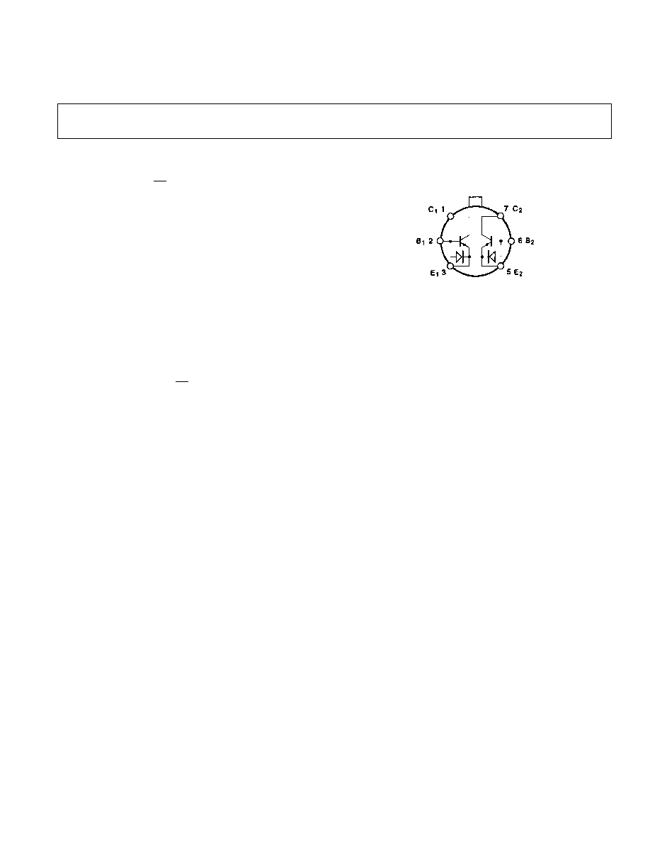
PIN CONNECTION
TO-78
(H Suffix)
GENERAL DESCRIPTION
The MAT03 dual monolithic PNP transistor offers excellent
parametric matching and high frequency performance. Low
noise characteristics (1 nV/
Hz
max @ 1 kHz), high bandwidth
(190 MHz typical), and low offset voltage (100
µ
V max), makes
the MAT03 an excellent choice for demanding preamplifier ap-
plications. Tight current gain matching (3% max mismatch) and
high current gain (100 min), over a wide range of collector cur-
rent, makes the MAT03 an excellent choice for current mirrors.
A low value of bulk resistance (typically 0.3
) also makes the
MAT03 an ideal component for applications requiring accurate
logarithmic conformance.
Each transistor is individually tested to data sheet specifications.
Device performance is guaranteed at 25
°
C and over the extended
industrial and military temperature ranges. To insure the long-
term stability of the matching parameters, internal protection
diodes across the base-emitter junction clamp any reverse base-
emitter junction potential. This prevents a base-emitter break-
down condition which can result in degradation of gain and
matching performance due to excessive breakdown current.
MAT03A
MAT03E
MAT03F
Parameter
Symbol
Conditions
Min
Typ
Max Min
Typ
Max
Min
Typ
Max
Units
Current Gain
1
h
FE
V
CB
= 0 V, 36 V
I
C
= 1 mA
100
165
100
165
80
165
I
C
= 100
µ
A
90
150
90
150
70
150
I
C
= 10
µ
A
80
120
80
120
60
120
Current Gain Matching
2
Dh
FE
I
C
= 100
µ
A,V
CB
= 0 V
0.5
3
0.5
3
0.5
6
%
Offset Voltage
3
V
OS
V
CB
= 0 V, I
C
= 100
µ
A
40
100
40
100
40
200
µ
V
Offset Voltage Change
DV
OS
/DV
CB
I
C
= 100
µ
A
vs. Collector Voltage
V
CB1
= 0 V
11
150
11
150
11
200
µ
V
V
CB2
= 36 V
11
150
11
150
11
200
µ
V
Offset Voltage Change
DV
OS
/DI
C
V
CB
= 0 V
12
50
12
50
12
75
µ
V
vs. Collector Current
I
C1
= 10
µ
A, I
C2
= 1 mA
12
50
12
50
12
75
µ
V
Bulk Resistance
r
BE
V
CB
= 0 V
0.3
0.75
0.3
0.75
0.3
0.75
10
µ
A
I
C
1 mA
0.3
0.75
0.3
0.75
0.3
0.75
Offset Current
I
OS
I
C
= 100
µ
A, V
CB
= 0 V
6
35
6
35
6
45
nA
Collector-Base
Leakage Current
I
CB0
V
CB
= 36 V = V
MAX
50
200
50
200
50
400
pA
Noise Voltage Density
4
e
N
I
C
= 1 mA, V
CB
= 0
f
O
= 10 Hz
0.8
2
0.8
0.8
nV/
÷
Hz
f
O
= 100 Hz
0.7
1
0.7
0.7
nV/
÷
Hz
f
O
= 1 kHz
0.7
1
0.7
0.7
nV/
÷
Hz
f
O
= 10 kHz
0.7
1
0.7
0.7
nV/
÷
Hz
Collector Saturation
Voltage
V
CE(SAT)
I
C
= 1 mA, I
B
= 100
µ
A
0.025 0.1
0.025 0.1
0.025 0.1
V
2
REV. B
NOTES
1
Current gain is measured at collector-base voltages (V
CB
) swept from 0 to V
MAX
at indicated collector current. Typicals are measured at V
CB
= 0 V.
2
Current gain matching (
h
FE
) is defined as:
h
FE =
100 (
I
B
) h
FE
(min )
I
C
.
3
Offset voltage is defined as: V
OS
= V
BE1
V
BE2
, where V
OS
is the differential voltage for I
C1
= I
C2
: V
OS
= V
BE1
V
BE2
=
KT
q
In
I
C1
I
C2
.
4
Sample tested. Noise tested and specified as equivalent input voltage for each transistor.
5
Guaranteed by V
OS
test (TCV
OS
=
V
OS
/T for V
OS
V
BE
) where T = 298
°
K for T
A
= 25
°
C.
Specifications subject to change without notice.
MAT03SPECIFICATIONS
ELECTRICAL CHARACTERISTICS
(@ T
A
= +25 C, unless otherwise noted.)
ELECTRICAL CHARACTERISTICS
MAT03A
Parameter
Symbol
Conditions
Min
Typ
Max
Units
Current Gain
h
FE
V
CB
= 0 V, 36 V
I
C
= 1 mA
70
110
I
C
= 100
µ
A
60
100
I
C
= 10
µ
A
50
85
Offset Voltage
V
OS
I
C
= 100
µ
A, V
CB
= 0 V
40
150
µ
V
Offset Voltage Drift
5
TCV
OS
I
C
= 100
µ
A, V
CB
= 0 V
0.3
0.5
µ
V/
°
C
Offset Current
I
OS
I
C
= 100
µ
A, V
CB
= 0 V
15
85
nA
Breakdown Voltage
BV
CEO
36
54
V
(at 55 C
T
A
+125 C, unless otherwise noted.)
ELECTRICAL CHARACTERISTICS
MAT03E
MAT03F
Parameter
Symbol
Conditions
Min
Typ
Max
Min
Typ
Max
Units
Current Gain
h
FE
V
CB
= 0 V, 36 V
I
C
= 1 mA
70
120
60
120
I
C
= 100
µ
A
60
105
50
105
I
C
= 10
µ
A
50
90
40
90
Offset Voltage
V
OS
I
C
= 100
µ
A, V
CB
= 0 V
30
135
30
265
µ
V
Offset Voltage Drift
5
TCV
OS
I
C
= 100
µ
A, V
CB
= 0 V
0.3
0.5
0.3
1.0
µ
V/
°
C
Offset Current
I
OS
I
C
= 100
µ
A, V
CB
= 0 V
10
85
10
200
nA
Breakdown Voltage
BV
CEO
36
36
V
(at 40 C
T
A
+85 C, unless otherwise noted.)

MAT03
3
REV. B
MAT03N
Parameter
Symbol
Conditions
Limits
Units
Breakdown Voltage
BV
CEO
36
V min
Offset Voltage
V
OS
I
C
= 100
µ
A, V
CB
= 0 V
200
µ
V max
10
µ
A
I
C
1 mA
200
µ
V max
Current Gain
h
FE
I
C
= 1 mA, V
CB
= 0 V, 36 V
80
min
I
C
= 10
µ
A, V
CB
= 0 V, 36 V
60
min
Current Gain Match
h
FE
I
C
= 100
µ
A, V
CB
= 0 V
6
% max
Offset Voltage Change vs. V
CB
V
OS
/
V
CB
V
CB1
= 0 V, I
C
= 100
µ
A
200
µ
V max
V
CB2
= 36 V
200
µ
V max
Offset Voltage Change
V
OS
/
I
C
V
CB
= 0
75
µ
V max
vs. Collector Current
I
C1
= 10
µ
A, I
C2
= 1 mA
75
µ
V max
Bulk Resistance
r
BE
10
µ
A
I
C
1 mA
0.75
max
Collector Saturation Voltage
V
CE (SAT)
I
C
= 1 mA, I
B
= 100
µ
A
0.1
V max
NOTE:
Electrical tests are performed at wafer probe to the limits shown. Due to variations in assembly methods and normal yield loss, yield after packaging is not guaranteed
for standard product dice. Consult factory to negotiate specifications based on dice lot qualification through sample lot assembly and testing.
WAFER TEST LIMITS
(at 25 C, unless otherwise noted.)
DICE CHARACTERISTICS
SUBSTRATE CAN BE
CONNECTED TO V OR
FLOATED
1. COLLECTOR (1 )
2. BASE (1 )
3. EMITTER (1 )
4. COLLECTOR (2)
5. BASE (2)
6. EMITTER (2 )
ABSOLUTE MAXIMUM RATINGS
1
Collector-Base Voltage (BV
CBO
) . . . . . . . . . . . . . . . . . . . . 36 V
Collector-Emitter Voltage (BV
CEO
) . . . . . . . . . . . . . . . . . . 36 V
Collector-Collector Voltage (BV
CC
) . . . . . . . . . . . . . . . . . . 36 V
Emitter-Emitter Voltage (BV
EE
) . . . . . . . . . . . . . . . . . . . . . 36 V
Collector Current (I
C
) . . . . . . . . . . . . . . . . . . . . . . . . . . 20 mA
Emitter Current (I
E
) . . . . . . . . . . . . . . . . . . . . . . . . . . . 20 mA
Total Power Dissipation
Ambient Temperature
70
°
C
2
. . . . . . . . . . . . . . . . 500 mW
Operating Temperature Range
MAT03A . . . . . . . . . . . . . . . . . . . . . . . . . . 55
°
C to +125
°
C
MAT03E/F . . . . . . . . . . . . . . . . . . . . . . . . . 40
°
C to +85
°
C
Operating Junction Temperature . . . . . . . . . . 55
°
C to +150
°
C
Storage Temperature . . . . . . . . . . . . . . . . . . . 65
°
C to +150
°
C
Lead Temperature (Soldering, 60 sec) . . . . . . . . . . . . . +300
°
C
Junction Temperature . . . . . . . . . . . . . . . . . . 65
°
C to +150
°
C
NOTES
1
Absolute maximum ratings apply to both DICE and packaged devices.
2
Rating applies to TO-78 not using a heat sink, and LCC; devices in free air only. For
TO-78, derate linearly at 6.3 mW/
°
C above 70
°
C ambient temperature; for LCC,
derate at 7.8 mW/
°
C.
ORDERING GUIDE
1
V
OS
max
Temperature
Package
Model
(T
A
= +25 C)
Range
Option
MAT03AH
2
100
µ
V
55
°
C to +125
°
C
TO-78
MAT03EH
100
µ
V
40
°
C to +85
°
C
TO-78
MAT03FH
200
µ
V
40
°
C to +85
°
C
TO-78
NOTES
1
Burn-in is available on industrial temperature range parts.
2
For devices processed in total compliance to MIL-STD-883, add/883 after part
number. Consult factory for 883 data sheet.
WARNING!
ESD SENSITIVE DEVICE
CAUTION
ESD (electrostatic discharge) sensitive device. Electrostatic charges as high as 4000 V readily
accumulate on the human body and test equipment and can discharge without detection.
Although the MAT03 features proprietary ESD protection circuitry, permanent damage may
occur on devices subjected to high energy electrostatic discharges. Therefore, proper ESD
precautions are recommended to avoid performance degradation or loss of functionality.
4
REV. B
MAT03
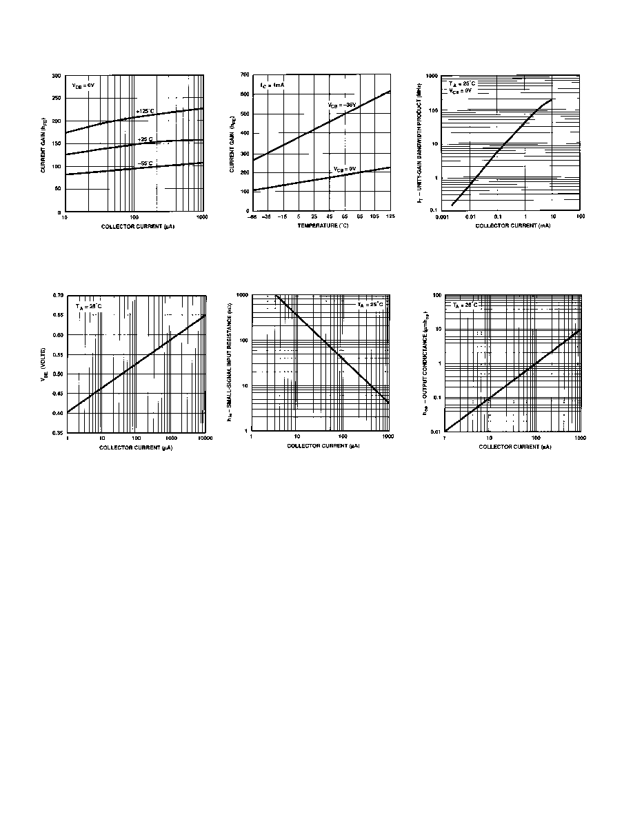
Figure 2. Current Gain
vs. Temperature
Figure 1. Current Gain vs.
Collector Current
Figure 3. Gain Bandwidth vs.
Collector Current
Figure 4. Base-Emitter Voltage
vs. Collector Current
Figure 5. Small-Signal Input Resistance
(h
ie
) vs. Collector Current
Figure 6. Small Signal Output Con-
ductance (h
oe
) vs. Collector Current
MAT03
5
REV. B
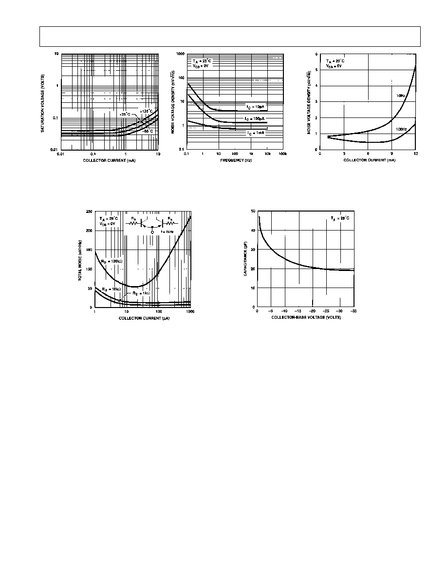
Figure 9. Noise Voltage Density
Figure 7. Saturation Voltage
vs. Collector Current
Figure 8. Noise Voltage Density
vs. Frequency
Figure 10. Total Noise vs. Collector Current
Figure 11. Collector-Base Capacitance vs. V
CB
6
REV. B
MAT03
Figure 12. SPICE or SABER Model
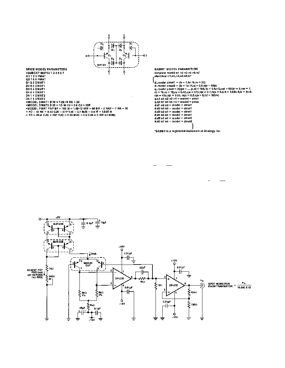
APPLICATIONS INFORMATION
MAT03 MODELS
The MAT03 model (Figure 12) includes parasitic diodes D
3
through D
6
. D
1
and D
2
are internal protection diodes which
prevent zenering of the base-emitter junctions.
The analysis programs, SPICE and SABER, are primarily used
in evaluating the functional performance of systems. The mod-
els are provided only as an aid in utilizing these simulation
programs.
MAT03 NOISE MEASUREMENT
All resistive components (Johnson noise, e
n
2
= 4kTBR, or e
n
=
0.13
R
nV/
Hz
, where R is in k
) and semiconductor junctions
(Shot noise, caused by current flowing through a junction, pro-
duces voltage noise in series impedances such as transistor-
collector load resistors, I
n
= 0.566
I
pA/
Hz
where I is in
µ
A)
contribute to the system input noise.
Figure 13 illustrates a technique for measuring the equivalent
input noise voltage of the MAT03. 1 mA of stage current is used
Figure 13. MAT03 Voltage Noise Measurement Circuit
MAT03
7
REV. B
to bias each side of the differential pair. The 5 k
collector re-
sistors noise contribution is insignificant compared to the volt-
age noise of the MAT03. Since noise in the signal path is
referred back to the input, this voltage noise is attenuated by the
gain of the circuit. Consequently, the noise contribution of the
collector load resistors is only 0.048 nV/
Hz
. This is consider-
ably less than the typical 0.8 nV/
Hz
input noise voltage of the
MAT03 transistor.
The noise contribution of the OP27 gain stages is also negligible
due to the gain in the signal path. The op amp stages amplify
the input referred noise of the transistors to increase the signal
strength to allow the noise spectral density (e
in
×
10000) to be
measured with a spectrum analyzer. And, since we assume
equal noise contributions from each transistor in the MAT03,
the output is divided by
2
to determine a single transistor's
input noise.
Air currents cause small temperature changes that can appear
as low frequency noise. To eliminate this noise source, the
measurement circuit must be thermally isolated. Effects of extrane-
ous noise sources must also be eliminated by totally shielding
the circuit.
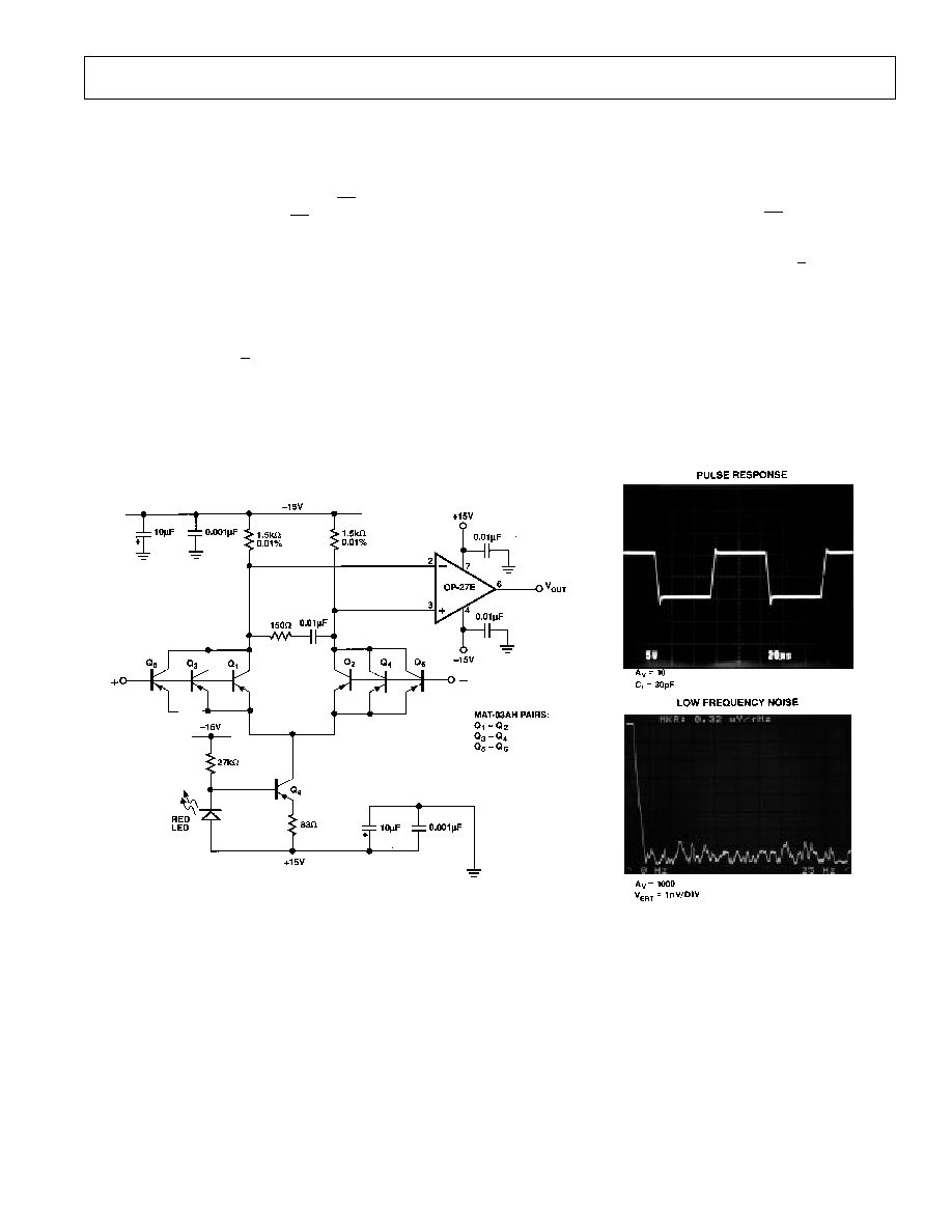
SUPER LOW NOISE AMPLIFIER
The circuit in Figure 14a is a super low noise amplifier with
equivalent input voltage noise of 0.32 nV/
Hz
. By paralleling
three MAT03 matched pairs, a further reduction of amplifier
noise is attained by a reduction of the base spreading resistance
by a factor of 3, and consequently the noise by
3
. Additionally,
the shot noise contribution is reduced by maintaining a high col-
lector current (2 mA/device) which reduces the dynamic emitter
resistance and decreases voltage noise. The voltage noise is in-
versely proportional to the square root of the stage current, and
current noise increases proportionally to the square root of the
stage current. Accordingly, this amplifier capitalizes on voltage
noise reduction techniques at the expense of increasing the cur-
rent noise. However, high current noise is not usually important
when dealing with low impedance sources.
Figure 14a. Super Low Noise Amplifier
8
REV. B
MAT03
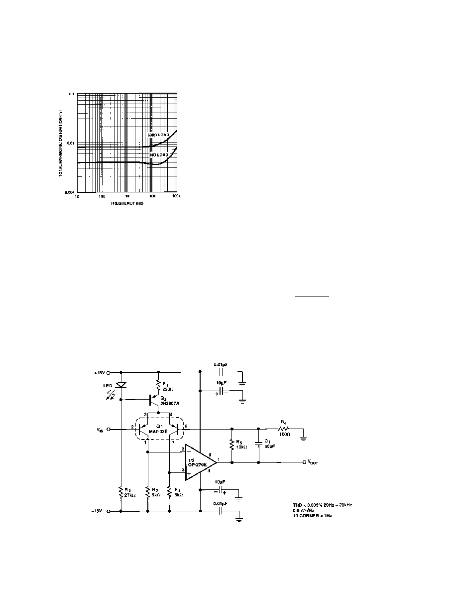
This amplifier exhibits excellent full power ac performance,
0.08% THD into a 600
load, making it suitable for exacting
audio applications (see Figure 14b).
Figure 14b. Super Low Noise Amplifier--Total
Harmonic Distortion
LOW NOISE MICROPHONE PREAMPLIFIER
Figure 15 shows a microphone preamplifier that consists of a
MAT03 and a low noise op amp. The input stage operates at a
relatively high quiescent current of 2 mA per side, which reduces
the MAT03 transistor's voltage noise. The 1/ corner is less than
1 Hz. Total harmonic distortion is under 0.005% for a 10 V p-p
signal from 20 Hz to 20 kHz. The preamp gain is 100, but can be
modified by varying R
5
or R
6
(V
OUT
/V
IN
= R
5
/R
6
+ 1).
A total input stage emitter current of 4 mA is provided by Q
2
.
The constant current in Q
2
is set by using the forward voltage of
a GaAsP LED as a reference. The difference between this voltage
and the V
BE
of a silicon transistor is predictable and constant (to
a few percent) over a wide temperature range. The voltage differ-
ence, approximately 1 V, is dropped across the 250
resistor
which produces a temperature stabilized emitter current.
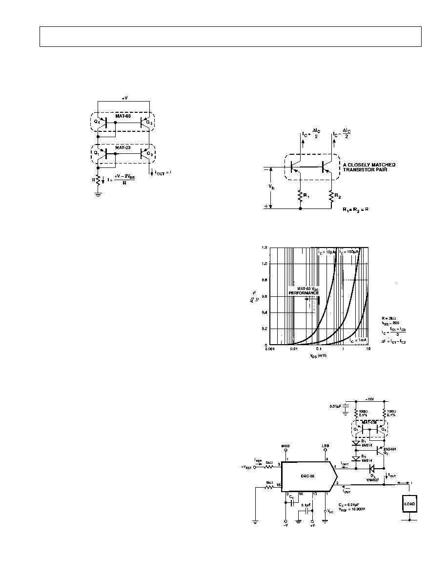
CURRENT SOURCES
A fundamental requirement for accurate current mirrors and ac-
tive load stages is matched transistor components. Due to the
excellent V
BE
matching (the voltage difference between V
BE
's
required to equalize collector current) and gain matching, the
MAT03 can be used to implement a variety of standard current
mirrors that can source current into a load such as an amplifier
stage. The advantages of current loads in amplifiers versus resis-
tors is an increase of voltage gain due to higher impedances,
larger signal range, and in many applications a wider signal
bandwidth.
Figure 16 illustrates a cascode current mirror consisting of two
MAT03 transistor pairs.
The cascode current source has a common base transistor in se-
ries with the output which causes an increase in output imped-
ance of the current source since V
CE
stays relatively constant.
High frequency characteristics are improved due to a reduction
of Miller capacitance. The small-signal output impedance can
be determined by consulting "h
OF
vs. Collector Current" typical
graph. Typical output impedance levels approach the perfor-
mance of a perfect current source.
Considering a typical collector current of 100
µ
A, we have:
ro
Q3
=
1
1.0
µ
MHOS
= 1 M
Figure 15. Low Noise Microphone Preamplifier
MAT03
9
REV. B
Q
2
and Q
3
are in series and operate at the same current levels so
the total output impedance is:
R
O
= h
FE
ro
Q3
@ (160)(1 M
) = 160 M
.
Figure 16. Cascode Current Source
CURRENT MATCHING
The objective of current source or mirror design is generation of
currents that are either matched or must maintain a constant ra-
tio. However, mismatch of base-emitter voltages cause output
current errors. Consider the example of Figure 17a. If the resis-
tors and transistors are equal and the collector voltages are the
same, the collector currents will match precisely. Investigating
the current-matching errors resulting from a nonzero V
OS
, we
define
I
C
as the current error between the two transistors.
Graph 17b describes the relationship of current matching errors
versus offset voltage for a specified average current I
C
. Note that
since the relative error between the currents is exponentially pro-
portional to the offset voltage, tight matching is required to de-
sign high accuracy current sources. For example, if the offset
voltage is 5 mV at 100
µ
A collector current, the current match-
ing error would be 20%. Additionally, temperature effects such
as offset drift (3
µ
V/
°
C per mV of V
OS
) will degrade performance
if Q
1
and Q
2
are not well matched.
DIGITALLY PROGRAMMABLE BIPOLAR CURRENT
PUMP
The circuit of Figure 18 is a digitally programmable current
pump. The current pump incorporates a DAC08, and a fast
Wilson current source using the MAT03. Examining Figure 18,
the DAC08 is set for 2 mA full-scale range so that bipolar cur-
rent operation of
±
2 mA is achieved. The Wilson current mirror
maintains linearity within the LSB range of the 8-bit DAC08
(
±
2 mA/256 = 15.6
µ
A resolution) as seen in Figure 19. A
negative feedback path established by Q
2
regulates the collector
current so that it matches the reference current programmed by
the DAC08.
Collector-emitter voltages across both Q
1
and Q
3
are matched
by D
1
, with Q
3
's collector-emitter voltage remaining constant,
independent of the voltage across the current source output.
Since Q
2
buffers Q
3
, both transistors in the MAT03, Q
1
and Q
3
,
maintain the same collector current. D
2
and D
3
form a Baker
clamp which prevents Q
2
from turning off, thereby improving
the switching speed of the current mirror. The feedback serves
to increase the output impedance and improves accuracy by re-
ducing the base-width modulation which occurs with varying
collector-emitter voltages. Accuracy and linearity performance
of the current pump is summarized in Figure 19.
Figure 17a. Current Matching Circuit
Figure 17b. Current Matching Accuracy %
vs. Offset Voltage
Figure 18. Digitally Programmable Bipolar Current Pump
10
REV. B
MAT03
Figure 19. Digitally Programmable Current
Pump--INL Error as Digital Code
The full-scale output of the DAC08, I
OUT
, is a linear function
of I
REF
I
FR
=
256
256
×
I
REF
, and I
OUT
+
I
OUT
= I
REF
256
256
The current mirror output is I
OUT
I
OUT
= 1, so that if
I
REF
= 2 mA:
I = 2 I
OUT
1.992 mA
= 2
Input Code
256
(2 mA) 1.992 mA.
DIGITAL CURRENT PUMP CODING
Digital Input
B1 . . . B8
Output Current
FULL RANGE
1111 1111
I = 1.992 mA
HALF-RANGE
1000 0000
I = 0.008 mA
ZERO-SCALE
0000 0000
I = 1.992 mA
MAT03
11
REV. B
OUTLINE DIMENSIONS
Dimensions shown in inches and (mm).
TO-78 Metal Can
0.250 (6.35) MIN
0.750 (19.05)
0.500 (12.70)
0.185 (4.70)
0.165 (4.19)
REFERENCE PLANE
0.050 (1.27) MAX
0.019 (0.48)
0.016 (0.41)
0.021 (0.53)
0.016 (0.41)
0.045 (1.14)
0.010 (0.25)
0.040 (1.02) MAX
BASE & SEATING PLANE
0.335 (8.51)
0.305 (7.75)
0.370 (9.40)
0.335 (8.51)
0.034 (0.86)
0.027 (0.69)
0.045 (1.14)
0.027 (0.69)
0.160 (4.06)
0.110 (2.79)
0.100 (2.54) BSC
5
2
6
4
3
1
0.200
(5.08)
BSC
0.100
(2.54)
BSC
45
°
BSC

12
000000000
PRINTED IN U.S.A.