 | –≠–ª–µ–∫—Ç—Ä–æ–Ω–Ω—ã–π –∫–æ–º–ø–æ–Ω–µ–Ω—Ç: OP250GS | –°–∫–∞—á–∞—Ç—å:  PDF PDF  ZIP ZIP |
PIN CONFIGURATIONS
8-Lead Narrow Body SO
(SO-8)
OP250
OUT A
≠IN A
+IN A
V≠
OUT B
≠IN B
+IN B
V+
1
2
3
4
8
7
6
5
(Not to Scale)
8-Lead TSSOP
(RU-8)
≠IN A
+IN A
V≠
OUT B
≠IN B
+IN B
V+
1
4
5
8
OUT A
OP250
14-Lead Narrow Body SO
(N-14)
OUT A
≠IN A
+IN A
V+
≠IN D
+IN D
V≠
OUT D
1
2
3
4
14
13
12
11
+IN B
≠IN B
OUT B
≠IN C
OUT C
+IN C
5
6
7
10
9
8
OP450
(Not to Scale)
14-Lead TSSOP
(RU-14)
AD8532
OUT A
≠IN A
+IN A
V+
≠IN D
+IN D
V≠
OUT D
1
14
+IN B
≠IN B
OUT B
≠IN C
OUT C
+IN C
7
8
OP450
1
14
7
8
REV. 0
Information furnished by Analog Devices is believed to be accurate and
reliable. However, no responsibility is assumed by Analog Devices for its
use, nor for any infringements of patents or other rights of third parties
which may result from its use. No license is granted by implication or
otherwise under any patent or patent rights of Analog Devices.
a
CMOS Single-Supply Rail-to-Rail
Input/Output Operational Amplifiers
OP250/OP450
One Technology Way, P.O. Box 9106, Norwood. MA 02062-9106, U.S.A.
Tel: 781/329-4700 World Wide Web Site: http://www.analog.com
Fax: 781/326-8703 © Analog Devices, Inc., 1997
FEATURES
Single-Supply Operation: 2.7 V to 6 V
High Output Current: 100 mA
Low Supply Current: 800 A/Amp
Wide Bandwidth: 1 MHz
Slew Rate: 2.2 V/ s
No Phase Reversal
Low Input Currents
Unity Gain Stable
APPLICATIONS
Battery Powered Instrumentation
Medical
Remote Sensors
ASIC Input or Output Amplifier
Automotive
GENERAL DESCRIPTION
The OP250 and OP450 are dual and quad CMOS single-supply,
amplifiers featuring rail-to-rail inputs and outputs. Both are guar-
anteed to operate from a +2.7 V to +5 V single supply.
These amplifiers have very low input bias currents. Outputs are
capable of driving 100 mA loads and are stable with capacitive
loads. Supply current is less than 1 mA per amplifier.
Applications for these amplifiers include portable medical
equipment, safety and security, and interface to transducers
with high output impedance.
The ability to swing rail-to-rail at both the input and output en-
ables designers to build multistage filters in single-supply sys-
tems and maintain high signal-to-noise ratios.
The OP250 and OP450 are specified over the extended indus-
trial (≠40
∞
C to +125
∞
C) temperature range. The OP250, dual,
is available in 8-lead TSSOP and SO surface mount packages.
The OP450, quad, is available in 14-lead thin shrink small out-
line (TSSOP) and narrow 14-lead SO packages.

REV. 0
≠2≠
OP250/OP450≠SPECIFICATIONS
ELECTRICAL CHARACTERISTICS
Parameter
Symbol
Conditions
Min
Typ
Max
Units
INPUT CHARACTERISTICS
Offset Voltage
V
OS
8
mV
≠40
∞
C < T
A
< +125
∞
C
20
mV
Input Bias Current
I
B
2
40
pA
≠40
∞
C < T
A
< +85
∞
C
60
pA
≠40
∞
C < T
A
< +125
∞
C
500
pA
Input Offset Current
I
OS
0.5
25
pA
≠40
∞
C < T
A
< +125
∞
C
60
pA
Input Voltage Range
0
3
V
Common-Mode Rejection Ratio
CMRR
V
CM
= 0 V to 3 V
40
55
dB
≠40
∞
C < T
A
< +125
∞
C
35
dB
Large Signal Voltage Gain
A
VO
R
L
= 2 k
, V
O
= 0.3 V to 2.7 V
800
V/mV
Offset Voltage Drift
V
OS
/
T
10
µ
V/
∞
C
Bias Current Drift
I
B
/
T
1.8
pA/
∞
C
Offset Current Drift
I
OS
/
T
0.07
pA/
∞
C
OUTPUT CHARACTERISTICS
Output Voltage High
V
OH
I
L
= 100
µ
A
2.99
V
I
L
= 10 mA
2.85
2.94
V
≠40
∞
C to +125
∞
C
2.8
V
Output Voltage Low
V
OL
I
L
= 100
µ
A
1
mV
I
L
= 10 mA
55
100
mV
≠40
∞
C to +125
∞
C
125
mV
Output Current
I
OUT
100
mA
Open Loop Impedance
Z
OUT
f = 1 MHz, A
V
= 1
180
POWER SUPPLY
Power Supply Rejection Ratio
PSRR
V
S
= 2.7 V to 6 V
60
80
dB
≠40
∞
C < T
A
< +125
∞
C
55
dB
Supply Current/Amplifier
I
SY
V
O
= 0 V
700
1,000
µ
A
≠40
∞
C < T
A
< +125
∞
C
1,250
µ
A
DYNAMIC PERFORMANCE
Slew Rate
SR
R
L
= 10 k
1.9
V/
µ
s
Settling Time
t
S
To 0.01%
4
µ
s
Gain Bandwidth Product
GBP
0.95
MHz
Phase Margin
ÿo
46
Degrees
Channel Separation
CS
f = 1 kHz, R
L
= 10 k
100
dB
NOISE PERFORMANCE
Voltage Noise
e
n
p≠p
0.1 Hz to 10 Hz
10
µ
V
p≠p
Voltage Noise Density
e
n
f = 1 kHz
45
nV/
Hz
f = 10 kHz
30
nV/
Hz
Current Noise Density
i
n
f = 1 kHz
0.05
pA/
Hz
Specifications subject to change without notice.
(V
S
= 3.0 V, T
A
= 25 C, V
CM
= 1.5 V unless otherwise noted)

ELECTRICAL CHARACTERISTICS
Parameter
Symbol
Conditions
Min
Typ
Max
Units
INPUT CHARACTERISTICS
Offset Voltage
V
OS
2
7.5
mV
≠40
∞
C < T
A
< +125
∞
C
20
mV
Input Bias Current
I
B
2
40
pA
≠40
∞
C < T
A
< +85
∞
C
60
pA
≠40
∞
C < T
A
< +125
∞
C
500
pA
Input Offset Current
I
OS
0.5
25
pA
≠40
∞
C < T
A
< +125
∞
C
60
pA
Input Voltage Range
0
5
V
Common-Mode Rejection Ratio
CMRR
V
CM
= 0 V to 5 V
45
60
dB
≠40
∞
C < T
A
< +125
∞
C
40
dB
Large Signal Voltage Gain
A
VO
R
L
= 2 k
, Vo = 0.3 V to 4.7 V
1,000
V/mV
Offset Voltage Drift
V
OS
/
T
≠40
∞
C < T
A
< +125
∞
C
10
µ
V/
∞
C
Bias Current Drift
I
B
/
T
1.8
pA/
∞
C
Offset Current Drift
I
OS
/
T
0.07
pA/
∞
C
OUTPUT CHARACTERISTICS
Output Voltage High
V
OH
I
L
= 100
µ
A
4.99
V
I
L
= 10 mA
4.9
4.94
V
≠40
∞
C to +125
∞
C
mV
Output Voltage Low
V
OL
I
L
= 100
µ
A
1
V
I
L
= 10 mA
40
100
mV
≠40
∞
C to +125
∞
C
125
mV
Output Current
I
OUT
±
100
mA
Open Loop Impedance
Z
OUT
f =1 MHz, A
V
= 1
200
POWER SUPPLY
Power Supply Rejection Ratio
PSRR
V
S
= 2.7 V to 6 V
60
80
dB
≠40
∞
C < T
A
< +125
∞
C
55
dB
Supply Current/Amplifier
I
SY
V
O
= 0 V
800
1,250
µ
A
≠40
∞
C < T
A
< +125
∞
C
750
1,750
µ
A
DYNAMIC PERFORMANCE
Slew Rate
SR
R
L
= 10 k
2.2
V/
µ
s
Full-Power Bandwidth
BW
P
1% Distortion
100
kHz
Settling Time
t
S
To 0.01%
3
µ
s
Gain Bandwidth Product
GBP
1
MHz
Phase Margin
ÿo
48
Degrees
Channel Separation
CS
f = 1 kHz, R
L
= 10 k
100
dB
NOISE PERFORMANCE
Voltage Noise
e
n
p≠p
0.1 Hz to 10 Hz
10
µ
V
p≠p
Voltage Noise Density
e
n
f = 1 kHz
45
nV/
Hz
f = 10 kHz
30
nV/
Hz
Current Noise Density
i
n
f = 1 kHz
0.05
pA/
Hz
Specifications subject to change without notice.
REV. 0
≠3≠
OP250/OP450
(V
S
= 5.0 V, T
A
= 25 C, V
CM
=2.5 V unless otherwise noted)

OP250/OP450
REV. 0
≠4≠
Package Type
JA
*
JC
Units
8-Lead SOIC (S)
158
43
∞
C/W
8-Lead TSSOP (RU)
240
43
∞
C/W
14-Lead SOIC (N)
120
36
∞
C/W
14-Lead TSSOP (RU)
180
35
∞
C/W
*
JA
is specified for the worst case conditions, i.e.,
JA
specified for device soldered
in circuit board for surface mount packages.
ABSOLUTE MAXIMUM RATINGS
1, 2
Supply Voltage . . . . . . . . . . . . . . . . . . . . . . . . . . . . . . . . . +6 V
Input Voltage
2
. . . . . . . . . . . . . . . . . . . . . . . . . . . . GND to V
S
Common-Mode Input Voltage . . . . . . . . . . . . . . . . . . . .
±
6 V
Output Short-Circuit
Duration to GND . . . . . . . . . . . . . Observe Derating Curves
ESD Susceptibility . . . . . . . . . . . . . . . . . . . . . . . . . . . . . 2000 V
Storage Temperature Range
S, RU Package . . . . . . . . . . . . . . . . . . . . .
65
∞
C to +150
∞
C
Operating Temperature Range
OP250G/OP450G . . . . . . . . . . . . . . . . . .
40
∞
C to +125
∞
C
Junction Temperature Range
S, RU Package . . . . . . . . . . . . . . . . . . . . .
65
∞
C to +150
∞
C
Lead Temperature Range (Soldering, 60 sec) . . . . . . . +300
∞
C
NOTES
1
Absolute maximum ratings apply at +25
∞
C, unless otherwise noted.
2
Stresses above those listed under Absolute Maximum Ratings may cause perma -
nent damage to the device. This is a stress rating only; the functional operation of
the device at these or any other conditions above those indicated in the opera tional
sections of this specification is not implied. Exposure to absolute maximum rating
conditions for extended periods may affect device reliability.
CAUTION
ESD (electrostatic discharge) sensitive device. Electrostatic charges as high as 4000 V readily
accumulate on the human body and test equipment and can discharge without detection. Although
the OP250/OP450 features proprietary ESD protection circuitry, permanent damage may occur on
devices subjected to high energy electrostatic discharges. Therefore, proper ESD precautions are
recommended to avoid performance degradation or loss of functionality.
ORDERING GUIDE
Temperature
Package
Package
Model
Range
Description
Options
OP250GS
≠40
∞
C to +125
∞
C
8-Lead SOIC
SO-8
OP250GRU
≠40
∞
C to +125
∞
C
8-Lead TSSOP
RU-8
OP450GS
≠40
∞
C to +125
∞
C
14-Lead SOIC
N-14
OP450GRU
≠40
∞
C to +125
∞
C
14-Lead TSSOP
RU-14
WARNING!
ESD SENSITIVE DEVICE
LOAD CURRENT ≠ mA
10k
10
0.1
0.001
100
0.01
OUTPUT VOLTAGE ≠ mV
0.1
1
10
1
100
1k
SOURCE
SINK
V
S
= +2.7V
T
A
= +25 C
Figure 1. Output Voltage to Supply Rail vs. Load Current
LOAD CURRENT ≠ mA
10
0.1
0.001
100
0.01
OUTPUT VOLTAGE ≠ mV
0.1
1
10
1
100
1k
SOURCE
SINK
V
S
= +5V
T
A
= +25 C
Figure 2. Output Voltage to Supply Rail vs. Load Current
TEMPERATURE ≠ C
0.85
0.8
0.65
≠55
145
≠5
SUPPLY CURRENT / AMPLIFIER ≠ mA
25
65
105
0.75
0.7
≠35
≠15
45
85
125
V
S
= +5V
V
S
= +3V
Figure 3. Supply Current per Amplifier vs. Temperature
Typical Performance Characteristics≠OP250/OP450
REV. 0
≠5≠
SUPPLY VOLTAGE ≠ V
0.9
0
0.75
3
1
SUPPLY CURRENT / AMPLIFIER ≠ mA
1.25
1.5
1.75
2
2.25
2.5
2.75
0.7
0.4
0.3
0.2
0.1
0.6
0.5
0.8
T
A
= +25 C
Figure 4. Supply Current per Amplifier vs. Supply Voltage
TEMPERATURE ≠ C
1
0.5
≠1
≠55
145
≠5
INPUT OFFSET VOLTAGE ≠ mV
25
65
105
0
≠0.5
≠35
≠15
45
85
125
V
S
= +5V
V
CM
= +2.5V
Figure 5. Input Offset Voltage vs. Temperature
TEMPERATURE ≠ C
400
300
0
≠55
145
≠5
INPUT BIAS CURRENT ≠ pA
25
65
105
200
100
≠35
≠15
45
85
125
V
S
= +5V, +3V
V
CM
= V
S
/2
Figure 6. Input Bias Current vs. Temperature
TEMPERATURE ≠ C
5
0
≠55
145
≠5
INPUT OFFSET CURRENT ≠ pA
25
65
105
≠35
≠15
45
85
125
V
S
= +5V, +3V
V
CM
= V
S
/2
4
3
2
1
Figure 7. Input Offset Current vs. Temperature
COMMON-MODE VOLTAGE ≠ V
2
1
≠1
0
5
1
INPUT BIAS CURRENT ≠ pA
2
3
4
0
V
S
= +5V, +3V
T
A
= +25 C
Figure 8. Input Bias Current vs. Common-Mode Voltage
FREQUENCY ≠ Hz
80
60
≠80
1k
100M
10k
GAIN ≠ dB
100k
1M
10M
40
20
≠60
0
≠20
≠40
0
≠45
≠360
≠90
≠135
≠315
≠180
≠225
≠270
PHASE SHIFT ≠ DEGREES
V
S
= +2.7V
R
L
= NO LOAD
T
A
= +25 C
Figure 9. Open-Loop Gain and Phase
FREQUENCY ≠ Hz
80
60
≠80
1k
100M
10k
GAIN ≠ dB
100k
1M
10M
40
20
≠60
0
≠20
≠40
0
≠45
≠360
≠90
≠135
≠315
≠180
≠225
≠270
PHASE SHIFT ≠ DEGREES
V
S
= +5V
R
L
= NO LOAD
T
A
= +25 C
Figure 10. Open-Loop Gain and Phase
FREQUENCY ≠ Hz
5
4
0
1
10k
10
OUTPUT SWING ≠ V
P≠P
100
1k
3
2
1
V
S
= +2.7V
R
L
= 2 k
V
IN
= 2.5 V
P≠P
T
A
= +25 C
Figure 11. Closed-Loop Output Voltage Swing vs. Frequency
FREQUENCY ≠ Hz
5
4
0
1
10k
10
OUTPUT SWING ≠ V
P≠P
100
1k
3
2
1
V
S
= +5.0V
R
L
= 2 k
V
IN
= 4.9 V
P≠P
T
A
= +25 C
Figure 12. Closed-Loop Output Voltage Swing vs. Frequency
OP250/OP450≠Typical Performance Characteristics
REV. 0
≠6≠
OP250/OP450
REV. 0
≠7≠
FREQUENCY ≠ Hz
400
350
0
10k
100k
IMPEDANCE ≠
1M
10M
100M
300
250
50
200
150
100
V
S
= +5V
R
L
= NO LOAD
T
A
= +25 C
A
V
= +1
1k
A
V
= +10
Figure 13. Closed-Loop Output Impedance vs. Frequency
FREQUENCY ≠ Hz
80
60
≠20
1
10k
10
COMMON-MODE REJECTION ≠ dB
100
1k
40
20
0
V
S
= +5V
T
A
= +25 C
≠10
10
30
50
70
Figure 14. Common-Mode Rejection vs. Frequency
FREQUENCY ≠ Hz
100
80
1k
10k
POWER SUPPLY REJECTION RATIO ≠ dB
100k
1M
10M
60
40
20
0
≠20
V
S
= +2.7V
T
A
= +25 C
+PSRR
100
≠PSRR
Figure 15. Power Supply Rejection vs. Frequency
FREQUENCY ≠ Hz
100
60
1k
10k
POWER SUPPLY REJECTION RATIO ≠ dB
100k
1M
10M
40
20
0
V
S
= +5V
T
A
= +25 C
+PSRR
100
≠PSRR
80
Figure 16. Power Supply Rejection vs. Frequency
CAPACITANCE ≠ pF
70
60
0
10
1k
100
SMALL SIGNAL OVERSHOOT ≠ %
50
40
30
20
10
V
S
= +2.7V
R
L
= 2 k
T
A
= +25 C
≠O
S
+O
S
Figure 17. Small Signal Overshoot vs. Load Capacitance
CAPACITANCE ≠ pF
70
60
0
10
1k
100
SMALL SIGNAL OVERSHOOT ≠ %
50
40
30
20
10
V
S
= +5.0V
R
L
= 2 k
T
A
= +25 C
≠O
S
+O
S
Figure 18. Small Signal Overshoot vs. Load Capacitance
25mV
2µs
V
S
= 1.35V
V
IN
= 50mV
A
V
= 1
R
L
= 2k
C
L
= 100pF
T
A
= 25 C
Figre 19. Small Signal Transient Response
25mV
2µs
V
S
= 2.5V
V
IN
= 50mV
A
V
= 1
R
L
= 2k
C
L
= 100pF
T
A
= 25 C
Figure 20. Small Signal Transient Response
500mV
2µs
V
S
= 1.35V
A
V
= 1
R
L
= 2k
T
A
= 25 C
Figure 21. Large Signal Transient Response
1V
2µs
V
S
= 2.5V
A
V
= 1
R
L
= 2k
T
A
= 25 C
Figure 22. Large Signal Transient Response
1V
50µs
Figure 23. No Phase Reversal
FREQUENCY ≠ Hz
1
0.1
0.01
10
100k
100
CURRENT NOISE DENSITY ≠ pA/
1k
10k
Figure 24. Current Noise Density vs. Frequency
OP250/OP450≠Typical Performance Characteristics
REV. 0
≠8≠

OP250/OP450
REV. 0
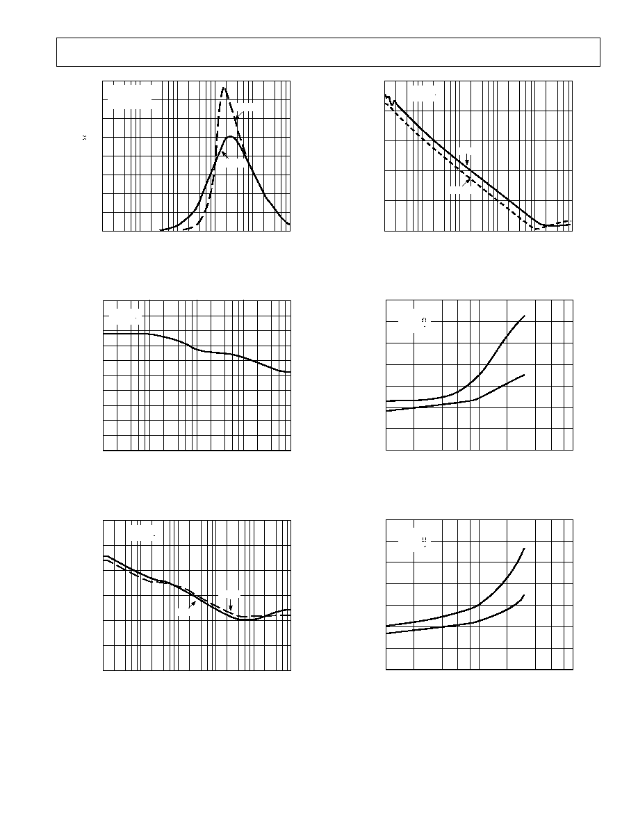
≠9≠
200nV
30nV/
V
S
= 5V
FREQUENCY = 10kHz
T
A
= 25 C
Figure 25. Voltage Noise Density vs. Frequency
100nV
45nV/
V
S
= 5V
FREQUENCY = 1kHz
T
A
= 25 C
Figure 26. Voltage Noise Density vs. Frequency
OP250/OP450
REV. 0
≠10≠
Output Phase Reversal
The OPx50 is immune to output voltage phase reversal with an
input voltage within the supply voltages of the device. However,
if either of the device's inputs exceeds 0.6 V outside of the sup-
ply rails, the output could exhibit phase reversal. This is due to
the ESD protection diodes becoming forward biased, thus caus-
ing the polarity of the input terminals of the device to switch.
The technique recommended in the Input Overvoltage Protec-
tion section should be applied in applications where the possibil-
ity of input voltages exceeding the supply voltages exists.
Output Short Circuit Protection
To achieve high quality rail-to-rail performance, the outputs of
the OPx50 family are not short-circuit protected. Although
these amplifiers are designed to sink or source as much as
250 mA of output current, shorting the output directly to
ground could damage or destroy the device when excessive volt-
ages or currents are applied. If to protect the output stage, the
maximum output current should be limited to
±
250 mA.
By placing a resistor in series with the output of the amplifier as
shown in Figure 28, the output current can be limited. The
minimum value for R
X
can be found from Equation 2.
R
V
mA
X
SY
250
(2)
For a +5 V single supply application, R
X
should be at least
20
. Because R
X
is inside the feedback loop, V
OUT
is not af-
fected. The trade-off in using R
X
is a slight reduction in output
voltage swing under heavy output current loads. R
X
will also
increase the effective output impedance of the amplifier to
R
O
+ R
X
, where R
O
is the output impedance of the device.
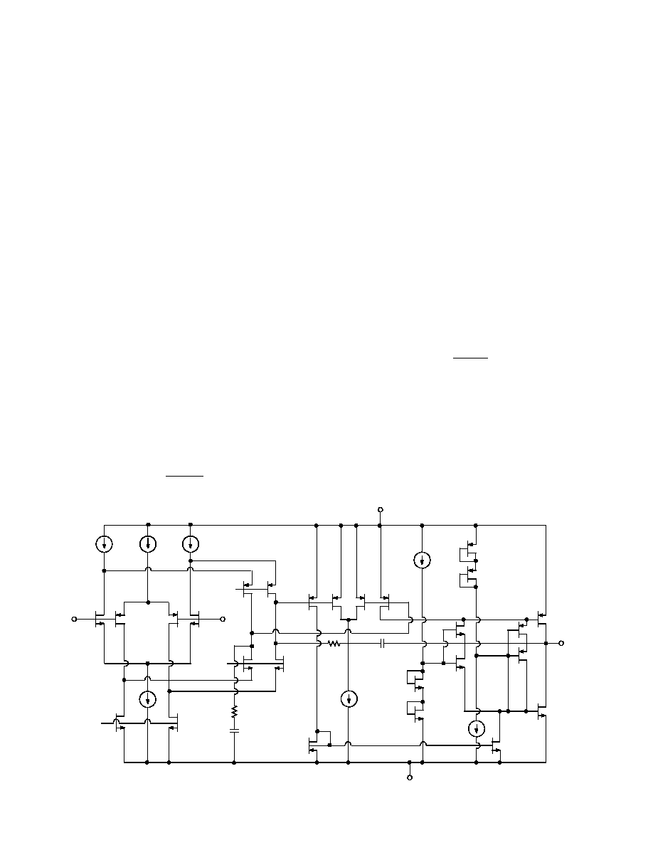
THEORY OF OPERATION
The OPx50 family of amplifiers are CMOS rail-to-rail input and
output single supply amplifiers designed for low cost and high
output current drive. These features make the OPx50 op amps
ideal for multimedia and telecom applications.
Figure 27 shows the simplified schematic for an OPx50 ampli-
fier. Two input differential pairs consisting of an n-channel pair
(M1≠M2) and a p-channel pair (M3≠M4) provide a rail-to-rail
input common-mode range. The outputs of the input differen-
tial pairs are combined in a compound folded-cascode stage,
which drives the input to a second differential pair gain stage.
The outputs of the second gain stage provide the gate voltage
drive to the rail-to-rail output stage.
The rail-to-rail output stage consists of M15 and M16, which
are configured in a complementary common-source configura-
tion. As with any rail-to-rail output amplifier, the gain of the
output stage, and thus the open loop gain of the amplifier, is de-
pendent on the load resistance. Also, the maximum output volt-
age swing is directly proportional to the load current. The
difference between the maximum output voltage to the supply
rails, known as the dropout voltage, is determined by the
OPx50's output transistors' on-channel resistance. The output
dropout voltage is given in Figures 1 and 2.
Input Voltage Protection
Although not shown on the simplified schematic, there are ESD
protection diodes connected from each input to each power supply
rail. These diodes are normally reversed biased, but will turn on if
either input voltage exceeds either supply rail by more than 0.6 V.
Should this condition occur the input current should be limited to
less than
±
5 mA. This can be done by placing a resistor in series
with the input. The minimum resistor value should be:
R
V
mA
IN
IN MAX
,
5
(1)
V
EE
V
CC
V
OUT
≠V
IN
+V
IN
M1
M2
M3
M4
BIAS
M5
M6
BIAS
BIAS
Figure 27. OPx50 Simplified Schematic
OP250/OP450
REV. 0
≠11≠
+5V
R
X
20
V
OUT
V
IN
OP250
Figure 28. Output Short-Circuit Protection
Power Dissipation
Although the OPx50 family of amplifiers are able to provide
load currents of up to 250 mA, proper attention should be given
to not exceed the maximum junction temperature for the device.
The equation for finding the junction temperature is given as:
T
J
JA
=
+
P
T
DISS
A
◊
(3)
Where
T
J
= OPx50 junction temperature
P
DISS
= OPx50 power dissipation
JA
= OPx50 junction-to-ambient thermal resistance of
the package; and
T
A
= The ambient temperature of the circuit
In any application, the absolute maximum junction temperature
must be limited to +150
∞
C. If this junction temperature is ex-
ceeded, the device could suffer premature failure. If the output
voltage and output current are in phase, for example, with a
purely resistive load, the power dissipated by the OPx50 can be
found as:
P
DISS
=
◊
-
(
)
I
V
V
LOAD
SY
OUT
(4)
Where
I
LOAD
= OPx50 output load current
V
SY
= OPx50 supply voltage; and
V
OUT
= The output voltage
By calculating the power dissipation of the device and using the
thermal resistance value for a given package type, the maximum
allowable ambient temperature for an application can be found
using Equation 3.
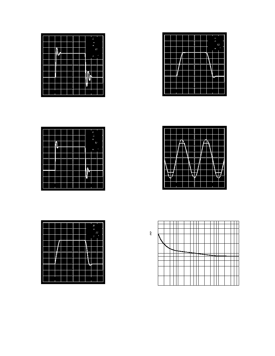
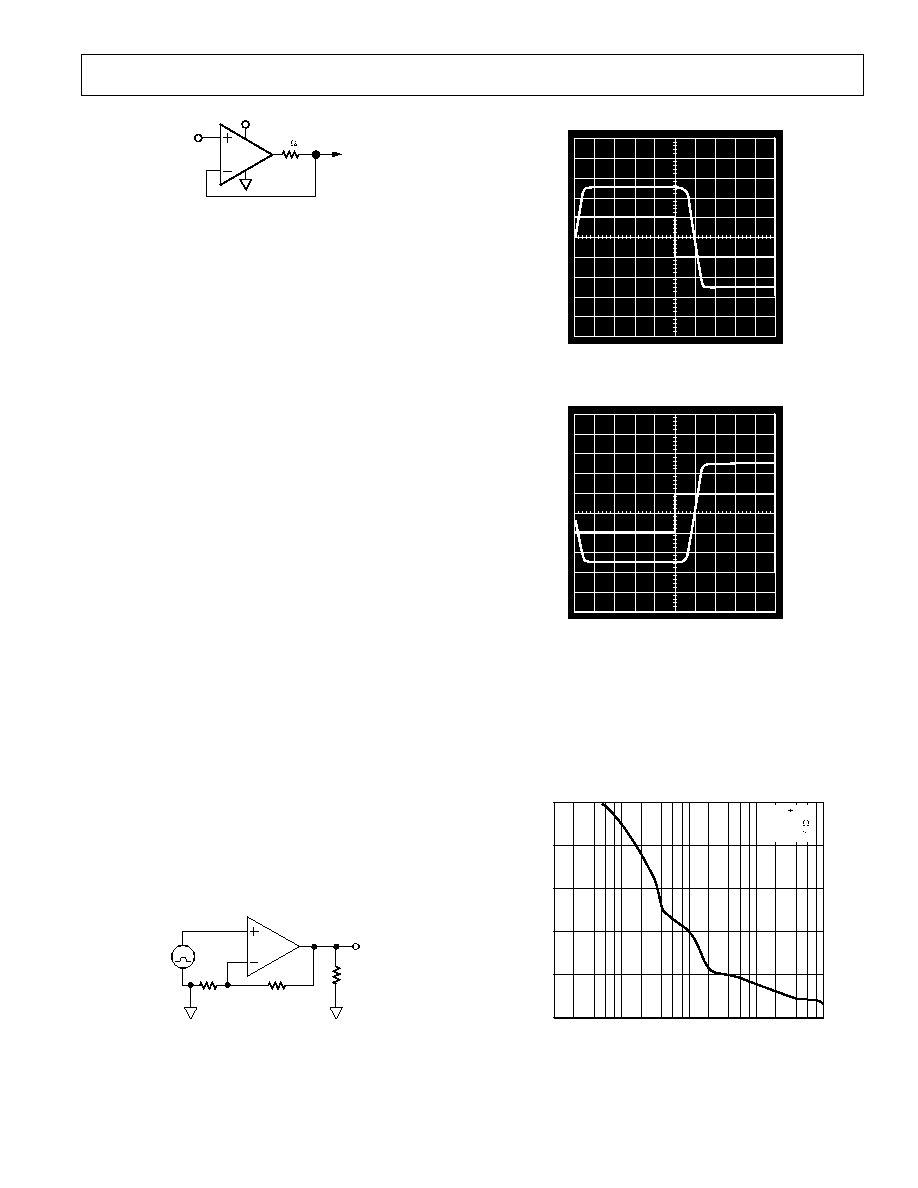
Overdrive Recovery
The overdrive, or overload, recovery time of an amplifier is the
time required for the output voltage to return to a rated output
voltage from a saturated condition. This recovery time can be
important in applications where the amplifier must recover
quickly after a large transient event. The circuit in Figure 29
was used to evaluate the recovery time for the OPx50. Figures
30 and 31 show the overload recovery of the OP250 from the
positive and negative rails. It takes approximately 0.5 ms for the
amplifier to recover from output overload.
OP250
10k
9k
1k
1V
P≠P
V
IN
V
OUT
Figure 29. Overload Recovery Time Test Circuit
1µs
500mV
Figure 30. Saturation Recovery from the Positive Rail
1µs
500mV
Figure 31. Saturation Recovery from the Negative Rail
Capacitive Loading
The OPx50 family of amplifiers is well suited to driving capaci-
tive loads. The device will remain stable at unity gain even un-
der heavy capacitive load conditions. However, a capacitive load
does not come without a penalty in bandwidth. Figure 32 shows
a graph of the OPx50 unity-gain bandwidth under various ca-
pacitive loads.
CAPACITIVE LOAD ≠ nF
1.0
0.8
0
0
1k
1
BANDWIDTH ≠ MHz
10
100
0.6
0.4
0.2
V
S
= 2.5V
R
L
= 10k
T
A
= +25 C
Figure 32. Unity-Gain Bandwidth vs. Capacitive Load
As with any amplifier, an increase in capacitive load will also re-
sult in an increase in overshoot and ringing. To improve the
output response, a series R-C network, known as a snubber, can
OP250/OP450
REV. 0
≠12≠
be connected from the output to ground in parallel with the ca-
pacitive load as shown in Figure 33. The proper snubber net-
work on the output can significantly reduce output overshoot,
although it will not increase the bandwidth. Table I shows some
snubber network values for a given capacitive load. In practice,
these values are best determined empirically based on the exact
capacitive load for the application.
+5V
R
S
5
V
OUT
V
IN
100mV p-p
OP250
C
L
47nF
C
S
1 F
Figure 33. Schematic for Using a Snubber Network
Table I. Snubber Network for Large Capacitive Loads
Load Capacitance (C
L
)
Snubber Network (RS, CS)
1 nF
60
, 30 nF
10 nF
20
, 1
µ
F
100 nF
3
, 10
µ
F
Figure 34 shows the output of an OP250 in a unity gain configu-
ration with a 1 nF capacitive load. Figure 35 shows the improve-
ment in the output response with the snubber network added.
2µs
50mV
C
L
= 1nF
R
L
= 10k
V
IN
= 100mV
p-p
@ 100kHz
Figure 34. Output of OP250 without Snubber Network
2µs
50mV
C
L
= 1nF
R
L
= 10k
V
IN
= 100mV
p-p
@ 100kHz
Figure 35. Output of OP250 with Snubber Network
For more information on methods to drive a capacitive load with
an op amp, please refer to the Ask the Applications Engineer ar-
ticle in Analog Dialogue, Vol. 31, Number 2, 1997.
Single Supply Differential Line Driver
Figure 36 shows a single supply differential line driver circuit
that can drive a 600
load with less than 0.1% distortion. The
design uses an OP450 to mimic the performance of a fully bal-
anced transformer based solution. However, this design occupies
much less board space while maintaining low distortion and can
operate down to dc. Like the transformer based design, either
output can be shorted to ground for unbalanced line driver ap-
plications without changing the circuit gain of 1.
R
L
600
C1
22 F
A2
7
6
5
3
1
2
A1
+5V
R1
10k
R2
10k
R11
10k
R7
10k
6
7
5
A1
+12V
+5V
R8
100k
R9
100k
C2
1 F
R12
10k
R14
50
A2
1
2
3
R3
10k
R6
10k
R13
10k
C3
47 F
V
O1
V
O2
C4
47µF
A1, A2 = 1/2 OP250
GAIN = R3
R2
SET: R7, R10, R11 = R2
SET: R6, R12, R13 = R3
V
IN
R10
10k
R5
50
Figure 36. A Low Noise, Single Supply Differential Line Driver
R8 and R9 set up the common mode output voltage equal to
half of the supply voltage. C1 is used to couple the input signal
and can be omitted if the input's dc voltage is equal to half of
the supply voltage.
The circuit can also be configured to provide additional gain if
desired. The gain of the circuit is:
A
V
V
R
R
V
OUT
IN
=
=
3
2
(5)
Where: V
OUT
= V
O1
≠ V
O2
,
R2 = R7 = R10 = R11 and,
R3 = R6 = R12 = R13
Multimedia Headphone Amplifier
Because of its large output drive, the OP250 makes an excellent
headphone amplifier, as illustrated in Figure 37. Its low supply
operation and rail-to-rail inputs and outputs can maximize out-
put signal swing on a single +5 V supply. In Figure 37, the am-
plifier inputs are biased halfway between the supply voltages,
which in this application is 2.5 V. A 10
µ
F capacitor prevents
power supply noise from contaminating the audio signal.

OP250/OP450
REV. 0
≠13≠
1/2
OP250
20
50k
270 F
LEFT
HEADPHONE
10 F
50k
50k
100k
10 F
LEFT
INPUT
+V + 5V
1/2
OP250
20
50k
270 F
RIGHT
HEADPHONE
10 F
50k
50k
100k
10 F
RIGHT
INPUT
+V
+V + 5V
1 F/0.1 F
Figure 37. A Single-Supply Stereo Headphone Driver
FREQUENCY ≠ Hz
1
0.1
0.001
20
20k
100
THD + N ≠ %
1k
0.01
10k
V
SY
= 2.5V
A
V
= +1
V
IN
= 300mV
rms
R
L
= 500
R
L
= 2k
R
L
10k
Figure 38. THD vs. Frequency
Headphone Driver
The audio signal is coupled into each input through a 10
µ
F ca-
pacitor. This large value insures the resulting high pass filter
cutoff is below 20 Hz, preserving full audio fidelity. If the input
already has the proper dc bias, then the coupling capacitor and
biasing resistors are not required. A 270
µ
F capacitor is used at
the output to couple the amplifier to the headphone speaker.
This value is much larger than the input capacitor because of
the low impedance of the headphones, which can range from
32
to 600
or more. An additional 20
resistor is used in
series with the output capacitor to protect the op amp's output
in the event the output accidentally becomes shorted to ground.
Direct Access Arrangement for Modems
Figure 39 illustrates a +5 V transmit/receive telephone line inter-
face for 600
systems. It allows full duplex transmission of sig-
nals on a transformer coupled 600
line in a differential manner.
Amplifier A1 provides gain which can be adjusted to meet the
modem output drive requirements. Both A1 and A2 are config-
ured so as to apply the largest possible signal on a single supply to
the transformer. Because of the OP450's high output current
drive and low dropout voltages, the largest signal available on a
single +5 V supply is approximately 4.5 V p-p into a 600
trans-
mission system. Amplifier A3 is configured as a difference ampli-
fier for two reasons: (1) It prevents the transmit signal from
interfering with the receive signal and (2) it extracts the receive
signal from the transmission line for amplification by A4. Ampli-
fier A4's gain can be adjusted in the same manner as A1's to meet
the modem's input signal requirements. Standard resistor values
permit the use of SIP (Single In-line Package) format resistor ar-
rays. Couple this with the OP450 14-lead TSSOP or SOIC foot-
print and this circuit offers a compact, cost-effective solution.
6.2V
6.2V
TRANSMIT
TXA
RECEIVE
RXA
C1
0.1 F
R1
10k
R2
9.09k
2k
P1
TX GAIN
ADJUST
A1
A2
A3
A4
A1, A2, A3, A4 = 1/4 OP450
R3
360
1:1
T1
TO TELEPHONE
LINE
1
2
3
7
6
5
2
3
1
6
5
7
10 F
R7
10k
R8
10k
R5
10k
R6
10k
R9
10k
R14
14.3k
R10
10k
R11
10k
R12
10k
R13
10k
C2
0.1 F
P2
RX GAIN
ADJUST
2k
Z
O
600
+5V DC
MIDCOM
671-8005
Figure 39. A Single-Supply Direct Access Arrangement for
Modems

OP250/OP450
REV. 0
≠14≠
* OP250 SPICE Macro-Model Typical Values
* 10/97, Ver. 1
* TAM / ADSC
*
* Node assignments
*
noninverting input
*
|
inverting input
*
|
|
positive supply
*
|
|
|
negative supply
*
|
|
|
|
output
*
|
|
|
|
|
*
|
|
|
|
|
.SUBCKT OP250 1
2
99
50
45
*
* INPUT STAGE
*
M1 4 3 6 6 MNIN L=2u W=66u
M2 5 2 6 6 MNIN L=2u W=66u
M3 7 3 9 9 MPIN L=2u W=66u
M4 8 2 9 9 MPIN L=2u W=66u
RD1 99 4 5E3
RD2 99 5 5E3
RD3 7 50 5E3
RD4 8 50 5E3
VCM1 10 50 -.3
VCM2 99 11 -.3
D1 10 6 DX
D2 9 11 DX
EOS 3 1 POLY(3) (61,98) (73,98) (81,0) 3E-3
+1 1 1
IOS 1 2 .25E-12
IBIAS1 6 50 700E-6
IBIAS2 99 9 700E-6
*
* CMRR=60 dB, ZERO AT 20kHz
*
ECM1 60 98 POLY(2) (1,98) (2,98) 0 .5 .5
RCM1 60 61 159.2E3
RCM2 61 98 159
CCM1 60 61 50E-12
*
* PSRR=90dB, ZERO AT 200Hz
*
RPS1 70 0 1E6
RPS2 71 0 1E6
CPS1 99 70 1E-5
CPS2 50 71 1E-5
EPSY 98 72 POLY(2) (70,0) (0,71) 0 1 1
RPS3 72 73 1.59E6
CPS3 72 73 500E-12
RPS4 73 98 50
*
* INTERNAL VOLTAGE REFERENCE
*
RSY1 99 91 100E3
RSY2 50 90 100E3
VSN1 91 90 DC 0
EREF 98 0 (90,0) 1
GSY 99 50 POLY(1) (99,50) -1.81E-3 1.5E-5
*
* VOLTAGE NOISE REFERENCE OF 30nV/rt(Hz)
*
VN1 80 0 0
RN1 80 0 16.45E-3
HN 81 0 VN1 30
RN2 81 0 1
*
* POLE AT 1.25MHz
*
G2 98 20 POLY(2) (4,5) (7,8) 0 5E-5 5E-5
R2 20 98 10E3
C2 20 98 12.7E-12
*
* GAIN STAGE
*
G1 98 30 (20,98) 3.5E-4
R1 30 98 6.25E6
CF 30 45 135E-12
D4 31 99 DX
D5 50 32 DX
V1 31 30 0.7
V2 30 32 0.7
*
* OUTPUT STAGE
*
M5 45 41 99 99 MPOUT L=2u W=6660u
M6 45 42 50 50 MNOUT L=2u W=6660u
EO1 99 41 POLY(1) (98,30) .9232 1
EO2 42 50 POLY(1) (30,98) .8914 1
*
* MODELS
*
.MODEL MNIN NMOS(LEVEL=2,VTO=0.75,
+KP=20E-6,CGSO=0,KF=2.5E-31,AF=1)
.MODEL MPIN PMOS(LEVEL=2,VTO=-0.75,
+KP=20E-6,CGSO=0,KF=2.5E-31,AF=1)
.MODEL MNOUT NMOS(LEVEL=2,VTO=0.75,
+KP=30E-6,LAMBDA=0.04,CGSO=0)
.MODEL MPOUT PMOS(LEVEL=2,VTO=-0.75,
+KP=20E-6,LAMBDA=0.04,CGSO=0)
.MODEL DX D(IS=1E-16)
.ENDS OP250
OP250/OP450
REV. 0
≠15≠
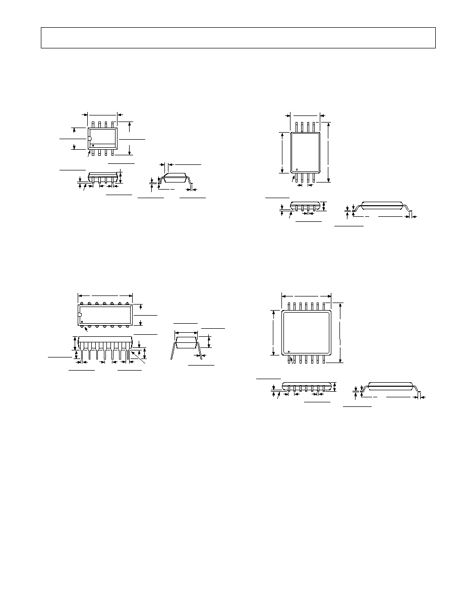
OUTLINE DIMENSIONS
Dimensions shown in inches and (mm).
8-Lead SOIC
(SO-8)
0.1968 (5.00)
0.1890 (4.80)
8
5
4
1
0.2440 (6.20)
0.2284 (5.80)
PIN 1
0.1574 (4.00)
0.1497 (3.80)
0.0688 (1.75)
0.0532 (1.35)
SEATING
PLANE
0.0098 (0.25)
0.0040 (0.10)
0.0192 (0.49)
0.0138 (0.35)
0.0500
(1.27)
BSC
0.0098 (0.25)
0.0075 (0.19)
0.0500 (1.27)
0.0160 (0.41)
8
∞
0
∞
0.0196 (0.50)
0.0099 (0.25)
x 45
∞
14-Lead Plastic DIP
(N-14)
14
1
7
8
0.795 (20.19)
0.725 (18.42)
0.280 (7.11)
0.240 (6.10)
PIN 1
0.325 (8.25)
0.300 (7.62)
0.015 (0.381)
0.008 (0.204)
0.195 (4.95)
0.115 (2.93)
SEATING
PLANE
0.022 (0.558)
0.014 (0.356)
0.060 (1.52)
0.015 (0.38)
0.210 (5.33)
MAX
0.130
(3.30)
MIN
0.070 (1.77)
0.045 (1.15)
0.100
(2.54)
BSC
0.160 (4.06)
0.115 (2.93)
8-Lead TSSOP
(RU-8)
8
5
4
1
0.122 (3.10)
0.114 (2.90)
0.256 (6.50)
0.246 (6.25)
0.177 (4.50)
0.169 (4.30)
PIN 1
0.0256 (0.65)
BSC
SEATING
PLANE
0.006 (0.15)
0.002 (0.05)
0.0118 (0.30)
0.0075 (0.19)
0.0433
(1.10)
MAX
0.0079 (0.20)
0.0035 (0.090)
0.028 (0.70)
0.020 (0.50)
8
∞
0
∞
14-Lead TSSOP
(RU-14)
14
8
7
1
0.201 (5.10)
0.193 (4.90)
0.256 (6.50)
0.246 (6.25)
0.177 (4.50)
0.169 (4.30)
PIN 1
SEATING
PLANE
0.006 (0.15)
0.002 (0.05)
0.0118 (0.30)
0.0075 (0.19)
0.0256
(0.65)
BSC
0.0433
(1.10)
MAX
0.0079 (0.20)
0.0035 (0.090)
0.028 (0.70)
0.020 (0.50)
8
∞
0
∞

C3236≠8≠10/97
PRINTED IN U.S.A.
≠16≠