 | –≠–ª–µ–∫—Ç—Ä–æ–Ω–Ω—ã–π –∫–æ–º–ø–æ–Ω–µ–Ω—Ç: OP275 | –°–∫–∞—á–∞—Ç—å:  PDF PDF  ZIP ZIP |

REV. A
Information furnished by Analog Devices is believed to be accurate and
reliable. However, no responsibility is assumed by Analog Devices for its
use, nor for any infringements of patents or other rights of third parties
which may result from its use. No license is granted by implication or
otherwise under any patent or patent rights of Analog Devices.
a
Dual Bipolar/JFET, Audio
Operational Amplifier
OP275*
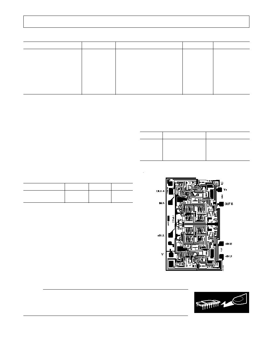
PIN CONNECTIONS
8-Lead Narrow-Body SO
8-Lead Epoxy DIP
(S Suffix)
(P Suffix)
OP275
OUT A
≠IN A
+IN A
V≠
OUT B
≠IN B
+IN B
V+
1
2
3
4
5
6
7
8
1
2
3
4
8
7
6
5
OP275
OUT B
≠IN B
+IN B
V+
OUT A
≠IN A
+IN A
V≠
Improved dc performance is also provided with bias and offset
currents greatly reduced over purely bipolar designs. Input off-
set voltage is guaranteed at 1 mV and is typically less than
200
µ
V. This allows the OP275 to be used in many dc coupled
or summing applications without the need for special selections
or the added noise of additional offset adjustment circuitry.
The output is capable of driving 600
loads to 10 V rms while
maintaining low distortion. THD + Noise at 3 V rms is a low
0.0006%.
The OP275 is specified over the extended industrial (≠40
∞
C to
+85
∞
C) temperature range. OP275s are available in both plastic
DIP and SOIC-8 packages. SOIC-8 packages are available in
2500 piece reels. Many audio amplifiers are not offered in
SOIC-8 surface mount packages for a variety of reasons; how-
ever, the OP275 was designed so that it would offer full perfor-
mance in surface mount packaging.
GENERAL DESCRIPTION
The OP275 is the first amplifier to feature the Butler Amplifier
front-end. This new front-end design combines both bipolar
and JFET transistors to attain amplifiers with the accuracy and
low noise performance of bipolar transistors, and the speed and
sound quality of JFETs. Total Harmonic Distortion plus Noise
equals that of previous audio amplifiers, but at much lower sup-
ply currents.
A very low l/f corner of below 6 Hz maintains a flat noise density
response. Whether noise is measured at either 30 Hz or 1 kHz,
it is only 6 nV/
Hz. The JFET portion of the input stage gives
the OP275 its high slew rates to keep distortion low, even when
large output swings are required, and the 22 V/
µ
s slew rate of
the OP275 is the fastest of any standard audio amplifier. Best of
all, this low noise and high speed are accomplished using less
than 5 mA of supply current, lower than any standard audio
amplifier.
*Protected by U.S. Patent No. 5,101,126.
© Analog Devices, Inc., 1995
One Technology Way, P.O. Box 9106, Norwood. MA 02062-9106, U.S.A.
Tel: 617/329-4700
Fax: 617/326-8703
FEATURES
Excellent Sonic Characteristics
Low Noise: 6 nV/
Hz
Low Distortion: 0.0006%
High Slew Rate: 22 V/ s
Wide Bandwidth: 9 MHz
Low Supply Current: 5 mA
Low Offset Voltage: 1 mV
Low Offset Current: 2 nA
Unity Gain Stable
SOIC-8 Package
APPLICATIONS
High Performance Audio
Active Filters
Fast Amplifiers
Integrators

ELECTRICAL CHARACTERISTICS
Parameter
Symbol
Conditions
Min
Typ
Max
Units
AUDIO PERFORMANCE
THD + Noise
V
IN
= 3 V rms,
R
L
= 2 k
, f = 1 kHz
0.006
%
Voltage Noise Density
e
n
f = 30 Hz
7
nV/
Hz
f = 1 kHz
6
nV/
Hz
Current Noise Density
i
n
f = 1 kHz
1.5
pA/
Hz
Headroom
THD + Noise
0.01%,
R
L
= 2 k
, V
S
=
±
18 V
>12.9
dBu
INPUT CHARACTERISTICS
Offset Voltage
V
OS
1
mV
≠40
∞
C
T
A
+85
∞
C
1.25
mV
Input Bias Current
I
B
V
CM
= 0 V
100
350
nA
V
CM
= 0 V, ≠40
∞
C
T
A
+85
∞
C
100
400
nA
Input Offset Current
I
OS
V
CM
= 0 V
2
50
nA
V
CM
= 0 V, ≠40
∞
C
T
A
+85
∞
C
2
100
nA
Input Voltage Range
V
CM
≠10.5
+10.5
V
Common-Mode Rejection Ratio
CMRR
V
CM
=
±
10.5 V,
≠40
∞
C
T
A
+85
∞
C
80
106
dB
Large Signal Voltage Gain
A
VO
R
L
= 2 k
250
V/mV
R
L
= 2 k
, ≠40
∞
C
T
A
+85
∞
C
175
V/mV
R
L
= 600
200
V/mV
Offset Voltage Drift
V
OS
/
T
2
µ
V/
∞
C
OUTPUT CHARACTERISTICS
Output Voltage Swing
V
O
R
L
= 2 k
≠13.5
±
13.9
+13.5
V
R
L
= 2 k
, ≠40
∞
C
T
A
+85
∞
C
≠13
±
13.9
+13
V
R
L
= 600
, V
S
=
±
18 V
+14, ≠16
V
POWER SUPPLY
Power Supply Rejection Ratio
PSRR
V
S
=
±
4.5 V to
±
18 V
85
111
dB
V
S
=
±
4.5 V to
±
18 V,
≠40
∞
C
T
A
+85
∞
C
80
dB
Supply Current
I
SY
V
S
=
±
4.5 V to
±
18 V, V
O
= 0 V,
R
L
=
, ≠40
∞
C
T
A
+85
∞
C
4
5
mA
V
S
=
±
22 V, V
O
= 0 V, R
L
=
,
≠40
∞
C
T
A
+85
∞
C
5.5
mA
Supply Voltage Range
V
S
±
4.5
±
22
V
DYNAMIC PERFORMANCE
Slew Rate
SR
R
L
= 2 k
15
22
V/
µ
s
Full-Power Bandwidth
BW
P
kHz
Gain Bandwidth Product
GBP
9
MHz
Phase Margin
¯
m
62
Degrees
Overshoot Factor
V
IN
= 100 mV, A
V
= +1,
R
L
= 600
, C
L
= 100 pF
10
%
Specifications subject to change without notice.
REV. A
≠2≠
OP275≠SPECIFICATIONS
(@ V
S
= 15.0 V, T
A
= +25 C unless otherwise noted)
OP275
REV. A
≠3≠
Parameter
Symbol
Conditions
Limit
Units
Offset Voltage
V
OS
1
mV max
Input Bias Current
I
B
V
CM
= 0 V
350
nA max
Input Offset Current
I
OS
V
CM
= 0 V
50
nA max
Input Voltage Range
1
V
CM
±
10.5
V min
Common-Mode Rejection Ratio
CMRR
V
CM
=
±
10.5 V
80
dB min
Power Supply Rejection Ratio
PSRR
V =
±
4.5 V to
±
18 V
85
dB min
Large Signal Voltage Gain
A
VO
R
L
= 2 k
250
V/mV min
Output Voltage Range
V
O
R
L
= 10 k
±
13.5
V min
Supply Current
I
SY
V
O
= 0 V, R
L
=
5
mA max
NOTES
Electrical tests and wafer probe to the limits shown. Due to variations in assembly methods and normal yield loss, yield after packaging is not guaranteed for standard
product dice. Consult factory to negotiate specifications based on dice lot qualifications through sample lot assembly and testing.
1
Guaranteed by CMRR test.
Specifications subject to change without notice.
WAFER TEST LIMITS
(@ V
S
= 15.0 V, T
A
= +25 C unless otherwise noted)
ABSOLUTE MAXIMUM RATINGS
1
Supply Voltage . . . . . . . . . . . . . . . . . . . . . . . . . . . . . . . .
±
22 V
Input Voltage
2
. . . . . . . . . . . . . . . . . . . . . . . . . . . . . . . .
±
22 V
Differential Input Voltage
2
. . . . . . . . . . . . . . . . . . . . . . .
±
7.5 V
Output Short-Circuit Duration to GND
3
. . . . . . . . . Indefinite
Storage Temperature Range
P, S Package . . . . . . . . . . . . . . . . . . . . . . . . ≠65
∞
C to +150
∞
C
Operating Temperature Range
OP275G . . . . . . . . . . . . . . . . . . . . . . . . . . . . ≠40
∞
C to +85
∞
C
Junction Temperature Range
P, S Package . . . . . . . . . . . . . . . . . . . . . . . . ≠65
∞
C to +150
∞
C
Lead Temperature Range (Soldering, 60 sec) . . . . . . . +300
∞
C
Package Type
JA
4
JC
Units
8-Pin Plastic DIP (P)
103
43
∞
C/W
8-Pin SOIC (S)
158
43
∞
C/W
NOTES
1
Absolute maximum ratings apply to both DICE and packaged parts, unless
otherwise noted.
2
For supply voltages greater than
±
22 V, the absolute maximum input voltage is
equal to the supply voltage.
3
Shorts to either supply may destroy the device. See data sheet for full details.
4
JA
is specified for the worst case conditions, i.e.,
JA
is specified for device in socket
for cerdip, P-DIP, and LCC packages;
JA
is specified for device soldered in circuit
board for SOIC package.
WARNING!
ESD SENSITIVE DEVICE
CAUTION
ESD (electrostatic discharge) sensitive device. Electrostatic charges as high as 4000 V readily
accumulate on the human body and test equipment and can discharge without detection.
Although the OP275 features proprietary ESD protection circuitry, permanent damage may
occur on devices subjected to high energy electrostatic discharges. Therefore, proper ESD
precautions are recommended to avoid performance degradation or loss of functionality.
ORDERING GUIDE
Model
Temperature Range
Package Option
OP275GP
≠40
∞
C to +85
∞
C
8-Pin Plastic DIP
OP275GS
≠40
∞
C to +85
∞
C
8-Pin SOIC
OP275GSR
≠40
∞
C to +85
∞
C
SO-8 Reel, 2500 pcs.
OP275GBC
+25
∞
C
DICE
DICE CHARACTERISTICS
Die Size 0.070
◊
0.108 in. (7,560 sq. mils)
Substrate is connected to V≠

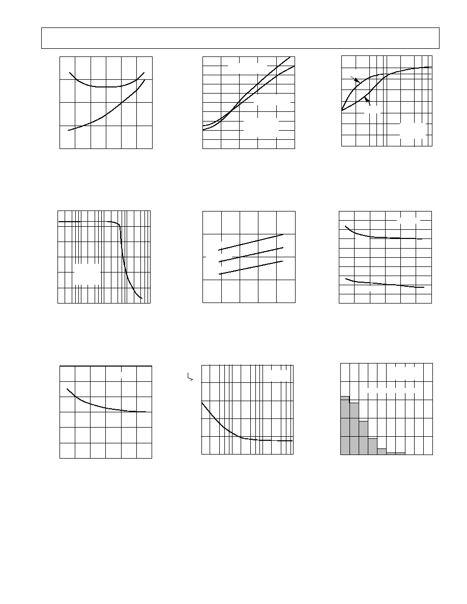
OP275≠Typical Performance Curves
REV. A
≠4≠
SUPPLY VOLTAGE ≠ V
OUTPUT VOLTAGE SWING ≠ V
25
20
≠25
0
±
5
±
25
±
10
±
15
±
20
≠5
≠10
≠15
≠20
15
5
10
0
T
A
= +25
∞
C
R
L
= 2k
+VOM
≠VOM
Output Voltage Swing vs. Supply
Voltage
FREQUENCY ≠ Hz
1M
10M
10k
100k
PHASE ≠ Degrees
135
90
45
0
≠45
≠90
60
50
≠20
40
30
20
10
0
≠10
GAIN ≠ dB
V
S
=
±
15V
T
A
= +25
∞
C
MARKER 15 309.059Hz
MAG (A/H) 60.115dB
MARKER 15 309.058Hz
PHASE (A/R 90.606Deg
Open-Loop Gain, Phase vs. Frequency
FREQUENCY ≠ Hz
120
100
0
100
1k
10M
10k
100k
1M
80
60
40
20
V
S
=
±
15V
T
A
= +25
∞
C
COMMON-MODE REJECTION ≠ dB
Common-Mode Rejection vs.
Frequency
TEMPERATURE ≠
∞
C
OPEN-LOOP GAIN ≠ V/mV
1500
0
≠50
≠25
100
0
25
50
75
1250
1000
750
500
250
V
S
=
±
15V
V
O
=
±
10V
+GAIN
R
L
= 2k
≠GAIN
R
L
= 2k
+GAIN
R
L
= 600
≠GAIN
R
L
= 600
Open-Loop Gain vs. Temperature
FREQUENCY ≠ Hz
50
CLOSED-LOOP GAIN ≠ dB
40
≠30
1k
10k
100M
100k
1M
10M
30
20
10
0
≠10
≠20
V
S
=
±
15V
T
A
= +25
∞
C
A
VCL
= +100
A
VCL
= +10
A
VCL
= +1
Closed-Loop Gain vs. Frequency
FREQUENCY ≠ Hz
120
100
0
10
100
1M
1k
10k
100k
80
60
40
20
POWER SUPPLY REJECTION ≠ dB
V
S
=
±
15V
T
A
= +25
∞
C
+PSRR
≠PSRR
Power Supply Rejection vs.
Frequency
FREQUENCY ≠ Hz
1M
10M
10k
100k
PHASE ≠ Degrees
180
135
≠180
90
45
0
≠45
≠90
≠135
40
30
≠40
20
10
0
≠10
≠20
≠30
GAIN ≠ dB
V
S
=
±
15V
T
A
= +25
∞
C
Closed-Loop Gain and Phase, A
V
= +1
FREQUENCY ≠ Hz
60
IMPEDANCE ≠
50
0
100
1k
10M
10k
100k
1M
40
30
20
10
V
S
=
±
15V
T
A
= +25
∞
C
A
VCL
= +1
A
VCL
= +10
A
VCL
= +100
Closed-Loop Output Impedance vs.
Frequency
FREQUENCY ≠ Hz
100
80
≠60
1k
10k
100M
100k
1M
10M
60
40
20
0
≠20
≠40
0
PHASE ≠ Degrees
45
90
135
180
225
270
V
S
=
±
15V
R
L
= 2k
T
A
= +25
∞
C
OPEN-LOOP GAIN ≠ dB
GAIN
PHASE
ÿ
m
= 58
∞
Open-Loop Gain, Phase vs. Frequency
OP275
REV. A
≠5≠
LOAD CAPACITANCE ≠ pF
100
OVERSHOOT ≠ %
90
0
0
100
500
200
300
400
40
30
20
10
80
60
70
50
A
VCL
= +1
NEGATIVE EDGE
A
VCL
= +1
POSITIVE EDGE
V
S
=
±
15V
R
L
= 2k
V
IN
= 100mV p-p
Small-Signal Overshoot vs. Load
Capacitance
SUPPLY VOLTAGE ≠ V
5.0
SUPPLY CURRENT ≠ mA
4.5
3.0
0
±
5
±
25
±
10
±
15
4.0
3.5
±
20
T
A
= +25
∞
C
T
A
= ≠40
∞
C
T
A
= +85
∞
C
Supply Current vs. Supply Voltage
FREQUENCY ≠ Hz
10
100
100k
1k
5
4
3
2
1
CURRENT NOISE DENSITY ≠ pA/
Hz
V
=
±
15V
T = +25
∞
C
S
A
Current Noise Density vs. Frequency
16
8
0
100
1k
10k
2
4
6
10
12
14
LOAD RESISTANCE ≠
T
A
= +25
∞
C
V
S
=
±
15V
+VOM
≠VOM
MAXIMUM OUTPUT SWING ≠ V
Maximum Output Voltage vs. Load
Resistance
TEMPERATURE ≠
∞
C
ABSOLUTE OUTPUT CURRENT ≠ mA
120
20
≠50
≠25
100
0
25
50
75
110
70
60
50
30
100
90
80
40
V
S
=
±
15V
SINK
SOURCE
Short Circuit Current vs. Temperature
TCV
OS
≠ µV/
∞
C
UNITS
500
400
0
0
1
10
2
3
4
5
6
7
8
9
300
200
100
BASED ON 920 OP AMPS
V
S
=
±
15V
≠40
∞
C to +85
∞
C
TCV
OS
Distribution
TEMPERATURE ≠
∞
C
GAIN BANDWIDTH PRODUCT ≠ MHz
11
10
7
≠50
≠25
100
0
25
50
75
9
8
PHASE MARGIN ≠ Degrees
65
60
40
55
50
GBW
ÿ
m
Gain Bandwidth Product, Phase
Margin vs. Temperature
25
20
15
10
5
FREQUENCY ≠ Hz
MAXIMUM OUTPUT SWING ≠ V
30
0
1k
10k
10M
100k
1M
T
A
= +25
∞
C
V
S
=
±
15V
A
VCL
= +1
R
L
= 2k
Maximum Output Swing vs.
Frequency
TEMPERATURE ≠
∞
C
300
INPUT BIAS CURRENT ≠ nA
0
≠50
≠25
100
0
25
50
75
250
200
150
100
50
V
S
=
±
15V
Input Bias Current vs. Temperature