 | –≠–ª–µ–∫—Ç—Ä–æ–Ω–Ω—ã–π –∫–æ–º–ø–æ–Ω–µ–Ω—Ç: OP27GS4 | –°–∫–∞—á–∞—Ç—å:  PDF PDF  ZIP ZIP |
REV. A
Information furnished by Analog Devices is believed to be accurate and
reliable. However, no responsibility is assumed by Analog Devices for its
use, nor for any infringements of patents or other rights of third parties that
may result from its use. No license is granted by implication or otherwise
under any patent or patent rights of Analog Devices.
a
OP27
One Technology Way, P.O. Box 9106, Norwood, MA 02062-9106, U.S.A.
Tel: 781/329-4700
www.analog.com
Fax: 781/326-8703
© Analog Devices, Inc., 2002
Low-Noise, Precision
Operational Amplifier
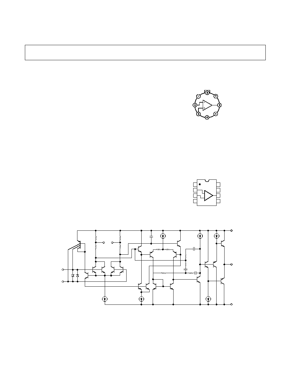
PIN CONNECTIONS
TO-99
(J-Suffix)
V+
OUT
NC
4V≠ (CASE)
BAL
BAL 1
≠IN 2
+IN 3
OP27
NC = NO CONNECT
FEATURES
Low Noise: 80 nV p-p (0.1 Hz to 10 Hz), 3 nV/
Hz
Low Drift: 0.2 V/ C
High Speed: 2.8 V/ s Slew Rate, 8 MHz Gain
Bandwidth
Low V
OS
: 10 V
Excellent CMRR: 126 dB at V
CM
of
±11 V
High Open-Loop Gain: 1.8 Million
Fits 725, OP07, 5534A Sockets
Available in Die Form
GENERAL DESCRIPTION
The OP27 precision operational amplifier combines the low
offset and drift of the OP07 with both high speed and low noise.
Offsets down to 25
µV and drift of 0.6 µV/∞C maximum make
the OP27 ideal for precision instrumentation applications.
Exceptionally low noise, e
n
= 3.5 nV/
Hz, at 10 Hz, a low 1/f
noise corner frequency of 2.7 Hz, and high gain (1.8 million),
allow accurate high-gain amplification of low-level signals. A
gain-bandwidth product of 8 MHz and a 2.8 V/
µsec slew rate
provides excellent dynamic accuracy in high-speed, data-
acquisition systems.
A low input bias current of
± 10 nA is achieved by use of a
bias-current-cancellation circuit. Over the military temperature
range, this circuit typically holds I
B
and I
OS
to
±20 nA and 15 nA,
respectively.
The output stage has good load driving capability. A guaranteed
swing of
±10 V into 600 and low output distortion make the
OP27 an excellent choice for professional audio applications.
(Continued on page 7)
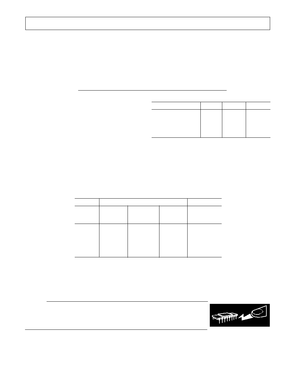
V≠
V+
Q2B
R2*
Q3
Q2A
Q1A
Q1B
R4
R1*
R3
1
8
V
OS
ADJ.
R1 AND R2 ARE PERMANENTLY
ADJUSTED AT WAFER TEST FOR
MINIMUM OFFSET VOLTAGE.
*
NONINVERTING
INPUT (+)
INVERTING
INPUT (≠)
Q6
Q21
C2
R23
R24
Q23
Q24
Q22
R5
Q11
Q12
Q27
Q28
C1
R9
R12
C3
C4
Q26
Q20
Q19
Q46
Q45
OUTPUT
Figure 1. Simplified Schematic
8-Pin Hermetic DIP
(Z-Suffix)
Epoxy Mini-DIP
(P-Suffix)
8-Pin SO
(S-Suffix)
8
7
6
5
1
2
3
4
NC = NO CONNECT
V
OS
TRIM
≠IN
+IN
V
OS
TRIM
V+
OUT
NC
V≠
OP27

REV. A
≠2≠
OP27
ELECTRICAL CHARACTERISTICS
OP27A/E
OP27F
OP27C/G
Parameter
Symbol
Conditions
Min
Typ
Max
Min
Typ
Max
Min
Typ
Max
Unit
INPUT OFFSET
VOLTAGE
1
V
OS
10
25
20
60
30
100
µV
LONG-TERM V
OS
STABILITY
2, 3
V
OS
/Time
0.2
1.0
0.3
1.5
0.4
2.0
µV/M
O
INPUT OFFSET
CURRENT
I
OS
7
35
9
50
12
75
nA
INPUT BIAS
CURRENT
I
B
±10
±40
±12
±55
±15
±80
nA
INPUT NOISE
VOLTAGE
3, 4
e
n p-p
0.1 Hz to 10 Hz
0.08
0.18
0.08
0.18
0.09
0.25
µV p-p
INPUT NOISE
e
n
f
O
= 10 Hz
3.5
5.5
3.5
5.5
3.8
8.0
nV/
Hz
Voltage Density
3
f
O
= 30 Hz
3.1
4.5
3.1
4.5
3.3
5.6
nV/
Hz
f
O
= 1000 Hz
3.0
3.8
3.0
3.8
3.2
4.5
nV/
Hz
INPUT NOISE
i
n
f
O
= 10 Hz
1.7
4.0
1.7
4.0
1.7
pA/
Hz
Current Density
3, 5
f
O
= 30 Hz
1.0
2.3
1.0
2.3
1.0
pA/
Hz
f
O
= 1000 Hz
0.4
0.6
0.4
0.6
0.4
0.6
pA/
Hz
INPUT
RESISTANCE
Differential-Mode
6
R
IN
1.3
6
0.94
5
0.7
4
M
Common-Mode
R
INCM
3
2.5
2
G
INPUT VOLTAGE
RANGE
IVR
±11.0 ±12.3
±11.0 ±12.3
±11.0 ±12.3
V
COMMON-MODE
REJECTION RATIO CMRR
V
CM
=
±11 V
114
126
106
123
100
120
dB
POWER SUPPLY
PSRR
V
S
=
±4 V
REJECTION RATIO
to
±18 V
1
10
1
10
2
20
µV/V
LARGE-SIGNAL
A
VO
R
L
2 k,
VOLTAGE GAIN
V
O
=
±10 V
1000
1800
1000
1800
700
1500
V/mV
R
L
600 ,
V
O
=
±10 V
800
1500
800
1500
600
1500
V/mV
OUTPUT
VOLTAGE SWING
V
O
R
L
2 k
±12.0 ±13.8
±12.0 ±13.8
±11.5 ±13.5
V
R
L
600
±10.0 ±11.5
±10.0 ±11.5
±10.0 ±11.5
V
SLEW RATE
7
SR
R
L
2 k
1.7
2.8
1.7
2.8
1.7
2.8
V/
µs
GAIN
BANDWIDTH
PRODUCT
7
GBW
5.0
8.0
5.0
8.0
5.0
8.0
MHz
OPEN-LOOP
OUTPUT
RESISTANCE
R
O
V
O
= 0, I
O
= 0
70
70
70
POWER
CONSUMPTION
P
d
V
O
90
140
90
140
100
170
mW
OFFSET
ADJUSTMENT
RANGE
R
P
= 10 k
±4.0
±4.0
±4.0
mV
NOTES
1
Input offset voltage measurements are performed ~ 0.5 seconds after application of power. A/E grades guaranteed fully warmed up.
2
Long-term input offset voltage stability refers to the average trend line of V
OS
versus. Time over extended periods after the first 30 days of operation. Excluding the
initial hour of operation, changes in V
OS
during the first 30 days are typically 2.5
µV. Refer to typical performance curve.
3
Sample tested.
4
See test circuit and frequency response curve for 0.1 Hz to 10 Hz tester.
5
See test circuit for current noise measurement.
6
Guaranteed by input bias current.
7
Guaranteed by design.
(@ V
S
=
±15 V, T
A
= 25 C, unless otherwise noted.)
≠SPECIFICATIONS

REV. A
≠3≠
OP27
(@ V
S
=
±15 V, ≠55 C T
A
125 C, unless otherwise noted.)
ELECTRICAL CHARACTERISTICS
OP27A
OP27C
Parameter
Symbol
Conditions
Min
Typ
Max
Min
Typ
Max
Unit
INPUT OFFSET
VOLTAGE
1
V
OS
30
60
70
300
µV
AVERAGE INPUT
OFFSET DRIFT
TCV
OS
2
TCV
OSn
3
0.2
0.6
4
1.8
µV/∞C
INPUT OFFSET
CURRENT
I
OS
15
50
30
135
nA
INPUT BIAS
CURRENT
I
B
±20
±60
±35
±150 nA
INPUT VOLTAGE
RANGE
IVR
±10.3
±11.5
±10.2
±11.5
V
COMMON-MODE
REJECTION RATIO CMRR
V
CM
=
±10 V
108
122
94
118
dB
POWER SUPPLY
REJECTION RATIO PSRR
V
S
=
±4.5 V to ±18 V
2
16
4
51
µV/V
LARGE-SIGNAL
VOLTAGE GAIN
A
VO
R
L
2 k, V
O
=
±10 V 600
1200
300
800
V/mV
OUTPUT
VOLTAGE SWING
V
O
R
L
2 k
±11.5
±13.5
±10.5
±13.0
V
NOTES
1
Input offset voltage measurements are performed by automated test equipment approximately 0.5 seconds after application of power. A/E grades guaranteed fully
warmed up.
2
The TCV
OS
performance is within the specifications unnulled or when nulled with R
P
= 8 k
to 20 k. TCV
OS
is 100% tested for A/E grades, sample tested for
C/F/G grades.
3
Guaranteed by design.

REV. A
≠4≠
OP27
ELECTRICAL CHARACTERISTICS
(@ V
S
=
±15 V, ≠25 CØ T
A
85 C for OP27J, OP27Z, 0 C T
A
70 C for OP27EP,
OP27FP, and ≠40 C
T
A
85 C for OP27GP, OP27GS, unless otherwise noted.)
OP27E
OP27F
OP27G
Parameter
Symbol
Conditions
Min
Typ
Max
Min
Typ
Max
Min
Typ
Max
Unit
INPUT ONSET
VOLTAGE
V
OS
20
50
40
140
55
220
µV
AVERAGE INPUT
OFFSET DRIFT
TCV
OS
1
0.2
0.6
0.3
1.3
0 4
1.8
µV/∞C
TCV
OSn
2
0.2
0.6
0.3
1.3
0 4
1.8
µV/∞C
INPUT OFFSET
CURRENT
I
OS
10
50
14
85
20
135
nA
INPUT BIAS
CURRENT
I
B
±14
±60
±18
±95
±25
±150 nA
INPUT VOLTAGE
RANGE
IVR
±10.5
±11.8
±10.5 ±11.8
±10.5 ±11.8
V
COMMON-MODE
REJECTION RATIO
CMRR
V
CM
=
±10 V
110
124
102
121
96
118
dB
POWER SUPPLY
REJECTION RATIO
PSRR
V
S
=
±4.5 V
2
15
2
16
2
32
µV/V
to
±18 V
LARGE-SIGNAL
VOLTAGE GAIN
A
VO
R
L
2 k,
V
O
=
±10 V
750
1500
700
1300
450
1000
V/mV
OUTPUT
VOLTAGE SWING
V
O
R
L
2 k
±11.7
±13.6
±11.4 ±13.5
±11.0 ±13.3
V
NOTES
1
The TCV
OS
performance is within the specifications unnulled or when nulled with R
P
= 8 k
to 20 k. TCV
OS
is 100% tested for A/E grades, sample tested for
C/F/G grades.
2
Guaranteed by design.
REV. A
≠5≠
OP27
OP27N
OP27G
OP27GR
Parameter
Symbol
Conditions
Limit
Limit
Limit
Unit
INPUT OFFSET VOLTAGE
*
V
OS
35
60
100
µV Max
INPUT OFFSET CURRENT
I
OS
35
50
75
nA Max
INPUT BIAS CURRENT
IB
±40
±55
±80
nA Max
INPUT VOLTAGE RANGE
IVR
±11
±11
±11
V Min
COMMON-MODE REJECTION
RATIO
CMRR
V
CM
= IVR
114
106
100
dB Min
POWER SUPPLY
PSRR
V
S
=
±4 V to ±18 V
10
10
20
µV/V Max
LARGE-SIGNAL VOLTAGE
GAIN
A
VO
R
L
2 k, V
O
=
±10 V
1000
1000
700
V/mV Min
A
VO
R
L
600 , V
O
=
±10 V
800
800
600
V/mV Min
OUTPUT VOLTAGE SWING
V
O
R
L
2 k
±12.0
±12.0
+11.5
V Min
V
O
RL2600n
±10.0
±10.0
±10.0
V Min
POWER CONSUMPTION
P
d
V
O
= 0
140
140
170
mW Max
NOTE
*Electrical tests are performed at wafer probe to the limits shown. Due to variations in assembly methods and normal yield loss, yield after packaging is not guaranteed
for standard product dice. Consult factory to negotiate specifications based on dice lot qualification through sample lot assembly and testing.
WAFER TEST LIMITS
(@ V
S
=
±15 V, T
A
= 25 C unless otherwise noted.)
DICE CHARACTERISTICS
1. NULL
2. (≠) INPUT
3. (+) INPUT
4. V≠
6. OUTPUT
7. V+
8. NULL
DIE SIZE 0.109 0.055 INCH, 5995 SQ. MILS
(2.77 1.40mm, 3.88 SQ. mm)

REV. A
≠6≠
OP27
OP27N
OP27G
OP27GR
Parameter
Symbol
Conditions
Typical
Typical
Typical
Unit
AVERAGE INPUT OFFSET
VOLTAGE DRIFT
*
TCV
OS
or
Nulled or Unnulled
0.2
0.3
0.4
µV/∞C
TCV
OSn
R
P
= 8 k
to 20 k
AVERAGE INPUT OFFSET
CURRENT DRIFT
TCI
OS
80
130
180
pA/
∞C
AVERAGE INPUT BIAS
CURRENT DRIFT
TCI
B
100
160
200
pA/
∞C
INPUT NOISE VOLTAGE
DENSITY
e
n
f
O
= 10 Hz
3.5
3.5
3.8
nV/
Hz
e
n
f
O
= 30 Hz
3.1
3.1
3.3
nV/
Hz
e
n
f
O
= 1000 Hz
3.0
3.0
3.2
nV/
Hz
INPUT NOISE CURRENT
DENSITY
i
n
f
O
= 10 Hz
1.7
1.7
1.7
pA/
Hz
i
n
f
O
= 30 Hz
1.0
1.0
1.0
pA/
Hz
i
n
f
O
= 1000 Hz
0.4
0.4
0.4
pA/
Hz
INPUT NOISE VOLTAGE
e
np-p
0.1 Hz to 10 Hz
0.08
0.08
0.09
µV p-p
SLEW RATE
SR
R
L
2 k
2.8
2.8
2.8
V/
µs
GAIN BANDWIDTH
PRODUCT
GBW
8
8
8
MHz
NOTE
*Input offset voltage measurements are performed by automated test equipment approximately 0.5 seconds after application of power.
TYPICAL ELECTRICAL CHARACTERISTICS
(@ V
S
=
±15 V, T
A
= 25 C unless otherwise noted.)
REV. A
OP27
≠7≠
Package Type
JA
3
JC
Unit
TO 99 (J)
150
18
∞C/W
8-Lead Hermetic DlP (Z)
148
16
∞C/W
8-Lead Plastic DIP (P)
103
43
∞C/W
20-Contact LCC (RC)
98
38
∞C/W
8-Lead SO (S)
158
43
∞C/W
NOTES
1
For supply voltages less than
± 22 V, the absolute maximum input voltage is
equal to the supply voltage.
2
The OP27's inputs are protected by back-to-back diodes. Current limiting
resistors are not used in order to achieve low noise. If differential input voltage
exceeds
± 0.7 V, the input current should be limited to 25 mA.
3
JA
is specified for worst-case mounting conditions, i.e.,
JA
is specified for
device in socket for TO, CERDIP, and P-DIP packages;
JA
is specified for
device soldered to printed circuit board for SO package.
4
Absolute Maximum Ratings apply to both DICE and packaged parts, unless
otherwise noted.
ABSOLUTE MAXIMUM RATINGS
4
Supply Voltage . . . . . . . . . . . . . . . . . . . . . . . . . . . . . . .
±22 V
Input Voltage
1
. . . . . . . . . . . . . . . . . . . . . . . . . . . . . . .
±22 V
Output Short-Circuit Duration . . . . . . . . . . . . . . . . Indefinite
Differential Input Voltage
2
. . . . . . . . . . . . . . . . . . . . . .
±0.7 V
Differential Input Current
2
. . . . . . . . . . . . . . . . . . . .
±25 mA
Storage Temperature Range . . . . . . . . . . . . ≠65
∞C to +150∞C
Operating Temperature Range
OP27A, OP27C (J, Z) . . . . . . . . . . . . . . . . ≠55
∞C to +125∞C
OP27E, OP27F (J, Z) . . . . . . . . . . . . . . . . . ≠25
∞C to +85∞C
OP27E, OP27F (P) . . . . . . . . . . . . . . . . . . . . . . 0
∞C to 70∞C
OP27G (P, S, J, Z) . . . . . . . . . . . . . . . . . . ≠40
∞C to +85∞C
Lead Temperature Range (Soldering, 60 sec) . . . . . . . 300
∞C
Junction Temperature . . . . . . . . . . . . . . . . . ≠65
∞C to +150∞C
ORDERING INFORMATION
1
Package
T
A
= 25
∞C
Operating
V
OS
Max
CERDIP
Plastic
Temperature
(
µV)
TO-99
8-Lead
8-Lead
Range
25
OP27AJ
2, 3
OP27AZ
2
MIL
25
OP27EJ
2, 3
OP27EZ
OP27EP
IND/COM
60
OP27FP
3
IND/COM
100
OP27CZ
3
MIL
100
OP27GJ
OP27GZ
OP27GP
XIND
100
OP27GS
4
XIND
NOTES
1
Burn-in is available on commercial and industrial temperature range parts in CERDIP, plastic
DIP, and TO-can packages.
2
For devices processed in total compliance to MIL-STD-883, add /883 after part number.
Consult factory for 883 data sheet.
3
Not for new design; obsolete April 2002.
4
For availability and burn-in information on SO and PLCC packages, contact your local
sales office.
CAUTION
ESD (electrostatic discharge) sensitive device. Electrostatic charges as high as 4000 V readily
accumulate on the human body and test equipment and can discharge without detection. Although
the OP27 features proprietary ESD protection circuitry, permanent damage may occur on devices
subjected to high-energy electrostatic discharges. Therefore, proper ESD precautions are
recommended to avoid performance degradation or loss of functionality.
WARNING!
ESD SENSITIVE DEVICE
(Continued from page 1)
PSRR and CMRR exceed 120 dB. These characteristics, coupled
with long-term drift of 0.2
µV/month, allow the circuit designer
to achieve performance levels previously attained only by dis-
crete designs.
Low-cost, high-volume production of OP27 is achieved by
using an on-chip Zener zap-trimming network. This reliable
and stable offset trimming scheme has proved its effectiveness
over many years of production history.
The OP27 provides excellent performance in low-noise, high-
accuracy amplification of low-level signals. Applications include
stable integrators, precision summing amplifiers, precision voltage-
threshold detectors, comparators, and professional audio circuits
such as tape-head and microphone preamplifiers.
The OP27 is a direct replacement for 725, OP06, OP07, and
OP45 amplifiers; 741 types may be directly replaced by remov-
ing the 741's nulling potentiometer.

REV. A
OP27
≠8≠
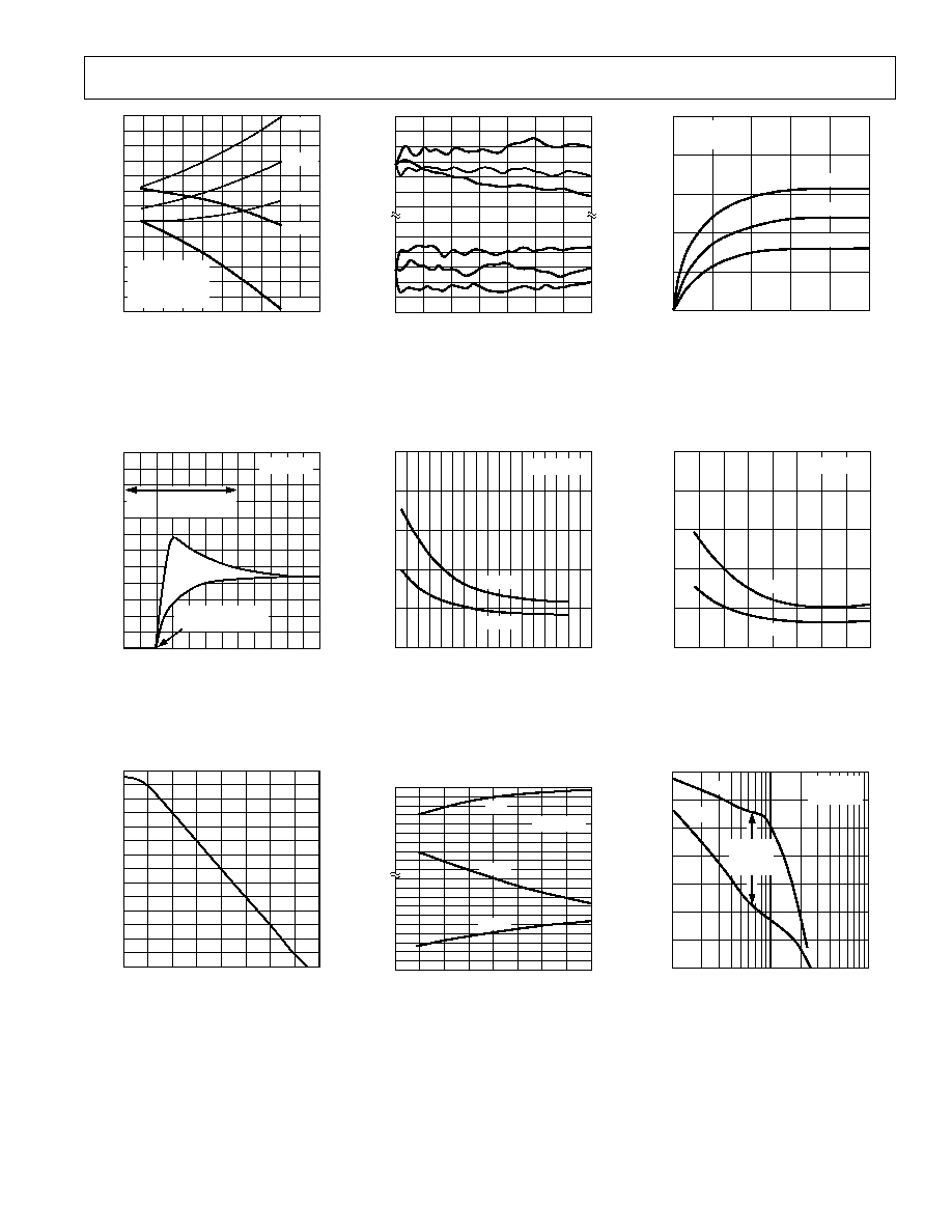
FREQUENCY ≠ Hz
GAIN
≠
dB
100
0.01
90
80
70
60
50
0.1
1
10
100
40
30
TEST TIME OF 10sec FURTHER
LIMITS LOW FREQUENCY
(<0.1Hz) GAIN
TPC 1. 0.1 Hz to 10 Hz
p-p
Noise Tester
Frequency Response
BANDWIDTH ≠ Hz
RMS V
O
L
T
A
GE
NOISE
≠
V
10
100k
1
0.1
0.01
100
1k
10k
T
A
= 25 C
V
S
= 15V
TPC 4. Input Wideband Voltage
Noise vs. Bandwidth (0.1 Hz to
Frequency Indicated)
TOTAL SUPPLY VOLTAGE (V+ ≠ V≠) ≠ V
V
O
L
T
A
GE NOISE
≠
nV/ Hz
5
4
1
0
10
40
20
30
3
2
T
A
= 25 C
AT 10Hz
AT 1kHz
TPC 7. Voltage Noise Density vs.
Supply Voltage
≠Typical Performance Characteristics
FREQUENCY ≠ Hz
10
1
T
A
= 25 C
V
S
= 15V
9
8
7
6
5
4
3
2
1
10
100
1k
V
O
L
T
A
GE NOISE
≠
nV/ Hz
I/F CORNER = 2.7Hz
TPC 2. Voltage Noise Density vs.
Frequency
SOURCE RESISTANCE ≠
100
1
10k
100
1k
T
O
T
A
L NOISE
≠
nV/ Hz
10
T
A
= 25 C
V
S
= 15V
R2
R1
R
S
≠ 2R1
AT 1kHz
AT 10Hz
RESISTOR NOISE ONLY
TPC 5. Total Noise vs. Sourced
Resistance
FREQUENCY ≠ Hz
CURRENT NOISE
≠
pA/ Hz
10.0
0.1
10
10k
1.0
100
1k
I/F CORNER = 140Hz
TPC 8. Current Noise Density vs.
Frequency
FREQUENCY ≠ Hz
100
1
1
10
100
1k
V
O
L
T
A
GE NOISE
≠
nV/ Hz
10
LOW NOISE
AUDIO OP AMP
INSTRUMENTATION
RANGE TO DC
AUDIO RANGE
TO 20kHz
I/F CORNER
741
OP27
I/F CORNER
I/F CORNER =
2.7Hz
TPC 3. A Comparison of Op Amp
Voltage Noise Spectra
TEMPERATURE ≠ C
V
O
L
T
A
GE NOISE
≠
nV/ Hz
5
≠50
≠25
0
25
50
75
100
125
4
3
2
1
AT 10Hz
AT 1kHz
V
S
= 15V
TPC 6. Voltage Noise Density vs.
Temperature
TOTAL SUPPLY VOLTAGE ≠ V
SUPPL
Y CURRENT
≠
mA
5.0
5
T
A
= +125 C
4.0
3.0
2.0
1.0
15
25
35
45
T
A
= +25 C
T
A
= ≠55 C
TPC 9. Supply Current vs. Supply
Voltage
REV. A
≠9≠
OP27
TEMPERATURE ≠ C
OFFSET V
O
L
T
A
GE
≠
V
60
≠75
40
20
0
≠20
≠40
≠60
≠50 ≠25
0
25
50
75 100 125 150 175
50
10
≠30
≠70
30
≠10
≠50
TRIMMING WITH
10k POT DOES
NOT CHANGE
TCV
OS
OP27C
OP27A
OP27A
OP27A
OP27C
TPC 10. Offset Voltage Drift of
Five Representative Units vs.
Temperature
TIME ≠ Sec
OPEN-LOOP GAIN
≠
dB
30
≠20
5
0
0
20
40
60
80
100
25
20
15
10
T
A
=
25 C
T
A
= 70 C
DEVICE IMMERSED
IN 70 C OIL BATH
V
S
= 15V
THERMAL
SHOCK
RESPONSE
BAND
TPC 13. Offset Voltage Change Due
to Thermal Shock
FREQUENCY ≠ Hz
V
O
L
T
A
GE GAIN
≠
dB
130
1
110
90
70
50
30
10
≠10
10
100
1k
10k 100k
1M 10M 100M
TPC 16. Open-Loop Gain vs.
Frequency
TIME ≠ Months
CHANGE IN OFFSET
V
O
L
T
A
GE
≠
V
6
0
2
≠2
≠6
4
0
≠2
≠6
1
2
3
4
5
6
7
4
0
≠4
6
2
≠4
TPC 11. Long-Term Offset Voltage
Drift of Six Representative Units
TEMPERATURE ≠ C
INPUT BIAS CURRENT
≠
nA
≠50
40
20
0
≠25
0
25
50
75
100 125 150
50
30
10
V
S
= 15V
OP27A
OP27C
TPC 14. Input Bias Current vs.
Temperature
TEMPERATURE ≠ C
SLEW RA
TE
≠
V/
s
≠50
60
2
≠25
0
25
50
75
100
125
4
V
S
= 15V
SLEW
50
70
3
PHASE MARGIN
≠
Degrees
10
9
8
7
6
GAIN B
AND
WIDTH PR
ODUCT
≠
MHz
GBW
≠75
M
TPC 17. Slew Rate, Gain-Bandwidth
Product, Phase Margin vs.
Temperature
TIME AFTER POWER ON ≠ Min
CHANGE IN INPUT OFFSET
V
O
L
T
A
GE
≠
V
10
1
0
1
4
2
3
5
T
A
= 25 C
V
S
= 15V
5
OP27 C/G
OP27 F
OP27 A/E
TPC 12. Warm-Up Offset Voltage
Drift
TEMPERATURE ≠ C
INPUT OFFSET CURRENT
≠
nA
≠75
50
0
≠50
≠25
0
25
50
75
100
125
V
S
= 15V
40
30
20
10
OP27A
OP27C
TPC 15. Input Offset Current vs.
Temperature
FREQUENCY ≠ Hz
25
1M
10M
100M
GAIN
≠
dB
20
15
10
5
0
≠5
≠10
80
100
120
140
160
180
200
220
PHASE SHIFT
≠
Degrees
T
A
= 25 C
V
S
= 15V
GAIN
PHASE
MARGIN
= 70
TPC 18. Gain, Phase Shift vs.
Frequency
REV. A
OP27
≠10≠
TOTAL SUPPLY VOLTAGE ≠ V
OPEN-LOOP GAIN
≠
V/
V
2.5
0
10
40
20
30
T
A
= 25 C
50
2.0
1.5
1.0
0.5
0
R
L
= 2k
R
L
= 1k
TPC 19. Open-Loop Voltage Gain vs.
Supply Voltage
CAPACITIVE LOAD ≠ pF
% O
VERSHOO
T
80
60
0
0
500
2000
1000
1500
40
20
V
S
= 15V
V
IN
= 100mV
A
V
= +1
100
2500
TPC 22. Small-Signal Overshoot vs.
Capacitive Load
TIME FROM OUTPUT SHORTED TO
GROUND ≠ Min
SHOR
T
-
CIRCUIT CURRENT
≠
mA
60
0
1
4
2
3
5
50
40
30
20
10
T
A
= 25 C
V
S
= 15V
I
SC
(+)
I
SC
(≠)
TPC 25. Short-Circuit Current vs.
Time
FREQUENCY ≠ Hz
28
1k
10k
100k
1M
PEAK-T
O
-PEAK AMPLITUDE
≠
V
24
20
16
12
8
4
0
T
A
= 25 C
V
S
= 15V
10M
TPC 20. Maximum Output Swing vs.
Frequency
20mV
500ns
50mV
0V
≠50mV
A
VCL
= +1
C
L
= 15pF
V
S
= 15V
T
A
= 25 C
TPC 23. Small-Signal Transient
Response
FREQUENCY ≠ Hz
CMRR
≠
dB
140
1k
120
100
80
60
10k
100k
1M
100
V
S
= 15V
T
A
= 25 C
V
CM
= 10V
TPC 26. CMRR vs. Frequency
LOAD RESISTANCE ≠
MAXIMUM OUTPUT
≠
V
18
100
1k
10k
16
14
12
10
8
6
4
2
0
≠2
T
A
= 25 C
V
S
= 15V
POSITIVE
SWING
NEGATIVE
SWING
TPC 21. Maximum Output Voltage
vs. Load Resistance
2V
2 s
+5V
0V
≠5V
A
VCL
= +1
V
S
= 15V
T
A
= 25 C
TPC 24. Large-Signal Transient
Response
SUPPLY VOLTAGE ≠ V
COMMON-MODE RANGE
≠
V
16
0
5
12
8
4
0
≠4
10
15
20
≠8
≠12
≠16
T
A
= ≠55 C
T
A
= +125 C
T
A
= +25 C
T
A
= +25 C
T
A
= ≠55 C
T
A
= +125 C
TPC 27. Common-Mode Input Range
vs. Supply Voltage

REV. A
≠11≠
OP27
OP12
OP27
D.U.T.
100k
4.3k
4.7 F
2k
24.3k
VOLTAGE
GAIN
= 50,000
2.2 F
22 F
110k
SCOPE 1
R
IN
= 1M
0.1 F
10
100k
0.1 F
TPC 28. Voltage Noise Test Circuit
(0.1 Hz to 10 Hz)
LOAD RESISTANCE ≠
2.4
100
1k
10k
100k
OPEN-LOOP V
O
L
T
A
GE
GAIN
≠
V/
V
T
A
= 25 C
V
S
= 15V
2.2
2.0
1.8
1.6
1.4
1.2
1.0
0.8
0.6
0.4
TPC 29. Open-Loop Voltage Gain vs.
Load Resistance
1 SEC/DIV
120
80
40
0
≠40
≠90
≠120
V
O
L
T
A
GE NOISE
≠
nV
0.1Hz to 10Hz p-p NOISE
TPC 30. Low-Frequency Noise
APPLICATION INFORMATION
OP27 series units may be inserted directly into 725 and OP07
sockets with or without removal of external compensation or
nulling components. Additionally, the OP27 may be fitted to
unnulled 741-type sockets; however, if conventional 741 nulling
circuitry is in use, it should be modified or removed to ensure
correct OP27 operation. OP27 offset voltage may be nulled to
zero (or another desired setting) using a potentiometer (see
Offset Nulling Circuit).
The OP27 provides stable operation with load capacitances of
up to 2000 pF and
±10 V swings; larger capacitances should be
decoupled with a 50
resistor inside the feedback loop. The
OP27 is unity-gain stable.
Thermoelectric voltages generated by dissimilar metals at the
input terminal contacts can degrade the drift performance. Best
operation will be obtained when both input contacts are main-
tained at the same temperature.
OFFSET VOLTAGE ADJUSTMENT
The input offset voltage of the OP27 is trimmed at wafer level.
However, if further adjustment of V
OS
is necessary, a 10 k
trim
potentiometer can be used. TCV
OS
is not degraded (see Offset
Nulling Circuit). Other potentiometer values from 1 k
to 1 M
can be used with a slight degradation (0.1
µV/∞C to 0.2 µV/∞C)
of TCV
OS
. Trimming to a value other than zero creates a drift of
approximately (V
OS
/300)
µV/∞C. For example, the change in
TCV
OS
will be 0.33
µV/∞C if V
OS
is adjusted to 100
µV. The
offset voltage adjustment range with a 10 k
potentiometer is
±4 mV. If smaller adjustment range is required, the nulling
sensitivity can be reduced by using a smaller pot in conjuction
with fixed resistors. For example, the network below will have a
±280 µV adjustment range.
1
8
4.7k
4.7k
1k
POT
V+
Figure 2.
NOISE MEASUREMENTS
To measure the 80 nV peak-to-peak noise specification of the
OP27 in the 0.1 Hz to 10 Hz range, the following precautions
must be observed:
1. The device must be warmed up for at least five minutes.
As shown in the warm-up drift curve, the offset voltage
typically changes 4
µV due to increasing chip temperature
after power-up. In the 10-second measurement interval,
these temperature-induced effects can exceed tens-of-
nanovolts.
2. For similar reasons, the device has to be well-shielded from
air currents. Shielding minimizes thermocouple effects.
FREQUENCY ≠ Hz
PO
WER SUPPL
Y REJECTION RA
TIO
≠
dB
140
1
T
A
= 25 C
120
100
80
60
40
20
0
10
100
1k
10k 100k 1M
10M 100M
160
POSITIVE
SWING
NEGATIVE
SWING
TPC 31. PSRR vs. Frequency

REV. A
OP27
≠12≠
3. Sudden motion in the vicinity of the device can also
"feedthrough" to increase the observed noise.
4. The test time to measure 0.1 Hz to 10 Hz noise should not
exceed 10 seconds. As shown in the noise-tester frequency
response curve, the 0.1 Hz corner is defined by only one
zero. The test time of 10 seconds acts as an additional zero
to eliminate noise contributions from the frequency band
below 0.1 Hz.
5. A noise-voltage-density test is recommended when measuring
noise on a large number of units. A 10 Hz noise-voltage-
density measurement will correlate well with a 0.1 Hz to 10 Hz
peak-to-peak noise reading, since both results are determined
by the white noise and the location of the 1/f corner frequency.
UNITY-GAIN BUFFER APPLICATIONS
When R
f
100 and the input is driven with a fast, large signal
pulse (>1 V), the output waveform will look as shown in the
pulsed operation diagram (Figure 3).
During the fast feedthrough-like portion of the output, the input
protection diodes effectively short the output to the input and a
current, limited only by the output short-circuit protection, will
be drawn by the signal generator. With R
f
500 , the output is
capable of handling the current requirements (I
L
20 mA at 10 V);
the amplifier will stay in its active mode and a smooth transition
will occur.
When R
f
> 2 k
, a pole will be created with R
f
and the amplifier's
input capacitance (8 pF) that creates additional phase shift and
reduces phase margin. A small capacitor (20 pF to 50 pF) in
parallel with R
f
will eliminate this problem.
+
≠
OP27
R
f
2.8V/ s
Figure 3. Pulsed Operation
COMMENTS ON NOISE
The OP27 is a very low-noise monolithic op amp. The outstanding
input voltage noise characteristics of the OP27 are achieved mainly
by operating the input stage at a high quiescent current. The input
bias and offset currents, which would normally increase, are held
to reasonable values by the input bias-current cancellation circuit.
The OP27A/E has I
B
and I
OS
of only
±40 nA and 35 nA at 25∞C
respectively. This is particularly important when the input has a
high source resistance. In addition, many audio amplifier design-
ers prefer to use direct coupling. The high I
B
, V
OS
, and TCV
OS
of previous designs have made direct coupling difficult, if not
impossible, to use.
Voltage noise is inversely proportional to the square root of bias
current, but current noise is proportional to the square root of
bias current. The OP27's noise advantage disappears when high
source-resistors are used. Figures 4, 5, and 6 compare OP27's
observed total noise with the noise performance of other devices
in different circuit applications.
Total Noise
Voltage Noise
Current Noise
R
sistor Noise
S
=
(
)
+
◊
(
)
+
(
)
2
2
2
1 2
Re
/
Figure 4 shows noise versus source-resistance at 1000 Hz. The
same plot applies to wideband noise. To use this plot, multiply
the vertical scale by the square root of the bandwidth.
R
S
≠ SOURCE RESISTANCE ≠
10
50
10k
T
O
T
A
L NOISE
≠
nV/ Hz
5
500
1k
5k
1
100
50
100
50k
R
S1
R
S2
1 R
S
UNMATCHED
e.g. R
S
= R
S1
= 10k , R
S2
= 0
2 R
S
MATCHED
e.g. R
S
= 10k , R
S1
= R
S2
= 5k
OP07
5534
OP27/37
REGISTER
NOISE ONLY
OP08/108
1
2
Figure 4. Noise vs. Source Resistance (Including Resistor
Noise) at 1000 Hz
At R
S
<1 k
, the OP27's low voltage noise is maintained. With
R
S
<1 k
, total noise increases, but is dominated by the resis-
tor noise rather than current or voltage noise. lt is only beyond
R
S
of 20 k
that current noise starts to dominate. The argument
can be made that current noise is not important for applica-
tions with low to moderate source resistances. The crossover
between the OP27, OP07, and OP08 noise occurs in the 15 k
to
40 k
region.
Figure 5 shows the 0.1 Hz to 10 Hz peak-to-peak noise. Here
the picture is less favorable; resistor noise is negligible and current
noise becomes important because it is inversely proportional to
the square root of frequency. The crossover with the OP07
occurs in the 3 k
to 5 k range depending on whether bal-
anced or unbalanced source resistors are used (at 3 k
the I
B
and I
OS
error also can be three times the V
OS
spec.).
R
S
≠ SOURCE RESISTANCE ≠
100
50
10k
p-p NOISE
≠
nV
50
500
1k
5k
10
1k
500
100
50k
R
S1
R
S2
1 R
S
UNMATCHED
e.g. R
S
= R
S1
= 10k , R
S2
= 0
2 R
S
MATCHED
e.g. R
S
= 10k , R
S1
= R
S2
= 5k
OP07
5534
OP27/37
REGISTER
NOISE ONLY
OP08/108
1
2
Figure 5. Peak-to-Peak Noise (0.1 Hz to 10 Hz) as Source
Resistance (Includes Resistor Noise)
REV. A
OP27
≠13≠
Therefore, for low-frequency applications, the OP07 is better
than the OP27/OP37 when R
S
> 3 k
. The only exception is
when gain error is important. Figure 6 illustrates the 10 Hz
noise. As expected, the results are between the previous two
figures.
For reference, typical source resistances of some signal sources
are listed in Table I.
Table I.
Source
Device
Impedance
Comments
Strain Gauge
<500
Typically used in low-
frequency applications.
Magnetic
<1500
Low is very important to
Tapehead
reduce self-magnetization
problems when direct coupling
is used. OP27 I
B
can be
neglected.
Magnetic
<1500
Similar need for low I
B
in
Phonograph
direct coupled applications.
Cartridges
OP27 will not introduce any
self-magnetization problem.
Linear Variable
<1500
Used in rugged servo-feedback
Differential
applications. Bandwidth of
Transformer
interest is 400 Hz to 5 kHz.
Open-Loop Gain
Frequency at
OP07
OP27
OP37
3 Hz
100 dB
124 dB
125 dB
10 Hz
100 dB
120 dB
125 dB
30 Hz
90 dB
110 dB
124 dB
For further information regarding noise calculations, see "Minimization of Noise
in Op Amp Applications," Application Note AN-15.
R
S
≠ SOURCE RESISTANCE ≠
10
50
10k
T
O
T
A
L NOISE
≠
nV/ Hz
5
500
1k
5k
1
100
50
100
50k
OP07
5534
OP27/37
REGISTER
NOISE ONLY
OP08/108
R
S1
R
S2
1 R
S
UNMATCHED
e.g. R
S
= R
S1
= 10k , R
S2
= 0
2 R
S
MATCHED
e.g. R
S
= 10k , R
S1
= R
S2
= 5k
1
2
Figure 6. 10 Hz Noise vs. Source Resistance (Includes
Resistor Noise)
AUDIO APPLICATIONS
The following applications information has been abstracted
from a PMI article in the 12/20/80 issue of Electronic De-
sign magazine and updated.
Figure 7 is an example of a phono pre-amplifier circuit using the
OP27 for A1; R1-R2-C1-C2 form a very accurate RIAA net-
work with standard component values. The popular method to
accomplish RIAA phono equalization is to employ frequency-
dependent feedback around a high-quality gain block. Properly
chosen, an RC network can provide the three necessary time
constants of 3180, 318, and 75
µs.
1
For initial equalization accuracy and stability, precision metal
film resistors and film capacitors of polystyrene or polypropy-
lene are recommended since they have low voltage coefficients,
dissipation factors, and dielectric absorption.
4
(High-K ceramic
capacitors should be avoided here, though low-K ceramics--
such as NPO types, which have excellent dissipation factors
and somewhat lower dielectric absorption--can be considered
for small values.)
Ca
150pF
A1
OP27
Ra
47.5k
R1
97.6k
MOVING MAGNET
CARTRIDGE INPUT
R2
7.87k
R3
100
C1
0.03 F
C2
0.01 F
C3
0.47 F
R4
75k
+
+
C4 (2)
220 F
LF ROLLOFF
OUT
IN
OUTPUT
R5
100k
G = 1kHz GAIN
= 0.101 (
)
R1
R3
1 +
= 98.677 (39.9dB) AS SHOWN
Figure 7.
The OP27 brings a 3.2 nV/
Hz voltage noise and 0.45 pA/Hz
current noise to this circuit. To minimize noise from other
sources, R3 is set to a value of 100
, which generates a voltage
noise of 1.3 nV/
Hz. The noise increases the 3.2 nV/Hz of the
amplifier by only 0.7 dB. With a 1 k
source, the circuit noise
measures 63 dB below a 1 mV reference level, unweighted, in a
20 kHz noise bandwidth.
Gain (G) of the circuit at 1 kHz can be calculated by the
expression:
G
R
R
=
+
0 101 1
1
3
.
For the values shown, the gain is just under 100 (or 40 dB).
Lower gains can be accommodated by increasing R3, but gains
higher than 40 dB will show more equalization errors because of
the 8 MHz gain-bandwidth of the OP27.
This circuit is capable of very low distortion over its entire range,
generally below 0.01% at levels up to 7 V rms. At 3 V output
levels, it will produce less than 0.03% total harmonic distortion
at frequencies up to 20 kHz.
Capacitor C3 and resistor R4 form a simple ≠6 dB-per-octave
rumble filter, with a corner at 22 Hz. As an option, the switch-
selected shunt capacitor C4, a nonpolarized electrolytic, bypasses
the low-frequency rolloff. Placing the rumble filter's high-pass
action after the preamp has the desirable result of discriminating
REV. A
OP27
≠14≠
against the RlAA-amplified low-frequency noise components and
pickup-produced low-frequency disturbances.
A preamplifier for NAB tape playback is similar to an RIAA
phono preamp, though more gain is typically demanded, along
with equalization requiring a heavy low-frequency boost. The
circuit in Figure 7 can be readily modified for tape use, as shown
by Figure 8.
Ca
Ra
R1
33k
TAPE
HEAD
0.47 F
0.01 F
R2
5k
100k
15k
T1 = 3180 s
T2 = 50 s
OP27
+
≠
Figure 8.
While the tape-equalization requirement has a flat high-frequency
gain above 3 kHz (T
2
= 50
µs), the amplifier need not be stabilized
for unity gain. The decompensated OP37 provides a greater
bandwidth and slew rate. For many applications, the idealized
time constants shown may require trimming of R1 and R2 to
optimize frequency response for nonideal tapehead performance
and other factors.
5
The network values of the configuration yield a 50 dB gain at
1 kHz, and the dc gain is greater than 70 dB. Thus, the worst-case
output offset is just over 500 mV. A single 0.47
µF output capaci-
tor can block this level without affecting the dynamic range.
The tapehead can be coupled directly to the amplifier input,
since the worst-case bias current of 80 nA with a 400 mH, 100
µ inch head (such as the PRB2H7K) will not be troublesome.
One potential tapehead problem is presented by amplifier bias-
current transients which can magnetize a head. The OP27 and
OP37 are free of bias-current transients upon power-up or power-
down. However, it is always advantageous to control the speed
of power supply rise and fall, to eliminate transients.
In addition, the dc resistance of the head should be carefully
controlled, and preferably below 1 kS2. For this configuration,
the bias-current-induced offset voltage can be greater than the
100pV maximum offset if the head resistance is not sufficiently
controlled.
A simple, but effective, fixed-gain transformerless microphone
preamp ( Figure 9) amplifies differential signals from low imped-
ance microphones by 50 dB, and has an input impedance of 2 k
.
Because of the high working gain of the circuit, an OP37 helps
to preserve bandwidth, which will be 110 kHz. As the OP37
is a decompensated device (minimum stable gain of 5), a dummy
resistor, Rp, may be necessary, if the microphone is to be
unplugged. Otherwise the 100% feedback from the open input
may cause the amplifier to oscillate.
Common-mode input-noise rejection will depend upon the
match of the bridge-resistor ratios. Either close-tolerance (0.1%)
types should be used, or R4 should be trimmed for best CMRR.
All resistors should be metal film types for best stability and
low noise.
Noise performance of this circuit is limited more by the input
resistors R1 and R2 than by the op amp, as R1 and R2 each gen-
erate a 4 nV/
Hz noise, while the op amp generates a 3.2 nV/Hz
noise. The rms sum of these predominant noise sources will be
about 6 nV/
Hz, equivalent to 0.9 µV in a 20 kHz noise band-
width, or nearly 61 dB below a 1 mV input signal. Measurements
confirm this predicted performance.
R3
316k
Rp
30k
R1
1k
R4
316k
R2
1k
R7
10k
R6
100
OUTPUT
R3
R1
R4
R2
=
LOW IMPEDANCE
MICROPHONE INPUT
(Z = 50 TO 200
)
C1
5 F
OP27/
OP37
+
≠
Figure 9.
For applications demanding appreciably lower noise, a high
quality microphone transformer-coupled preamp (Figure 10)
incorporates the internally compensated OP27. T1 is a JE-115K-E
150
/15 k transformer which provides an optimum source
resistance for the OP27 device. The circuit has an overall gain of
40 dB, the product of the transformer's voltage setup and the op
amp's voltage gain.
A1
OP27
R3
100
R1
121
R2
1100
C2
1800pF
OUTPUT
150
SOURCE
T1*
T1 ≠ JENSEN JE ≠ 115K ≠ E
JENSEN TRANSFORMERS
10735 BURBANK BLVD.
N. HOLLYWOOD, CA 91601
*
Figure 10.
Gain may be trimmed to other levels, if desired, by adjusting R2
or R1. Because of the low offset voltage of the OP27, the output
offset of this circuit will be very low, 1.7 mV or less, for a 40 dB
gain. The typical output blocking capacitor can be eliminated in
such cases, but is desirable for higher gains to eliminate switch-
ing transients.
OP27
≠18V
+18V
Figure 11. Burn-In Circuit
Capacitor C2 and resistor R2 form a 2
µs time constant in this
circuit, as recommended for optimum transient response by the
transformer manufacturer. With C2 in use, A1 must have unity-
gain stability. For situations where the 2
µs time constant is not
necessary, C2 can be deleted, allowing the faster OP37 to be
employed.

REV. A
OP27
≠15≠
Some comment on noise is appropriate to understand the
capability of this circuit. A 150
resistor and R1 and R2
gain resistors connected to a noiseless amplifier will generate
220 nV of noise in a 20 kHz bandwidth, or 73 dB below a 1 mV
reference level. Any practical amplifier can only approach this noise
level; it can never exceed it. With the OP27 and T1 specified, the
additional noise degradation will be close to 3.6 dB (or ≠69.5 refer-
enced to 1 mV).
OP27
V≠
INPUT
V+
OUTPUT
R
P
10k
Figure 12. Offset Nulling Circuit
References
1. Lipshitz, S.R, "On RIAA Equalization Networks," JAES,
Vol. 27, June 1979, p. 458≠481.
2. Jung, W.G., IC Op Amp Cookbook, 2nd. Ed., H.W. Sams and
Company, 1980.
3. Jung, W.G., Audio IC Op Amp Applications, 2nd. Ed., H.W.
Sams and Company, 1978.
4. Jung, W.G., and Marsh, R.M., "Picking Capacitors," Audio,
February and March, 1980.
5. Otala, M., "Feedback-Generated Phase Nonlinearity in
Audio Amplifiers," London AES Convention, March 1980,
preprint 1976.
6. Stout, D.F., and Kautman, M., Handbook of Operational
Amplifier Circuit Design, New York, McGraw-Hill, 1976.
OUTLINE DIMENSIONS
Dimensions shown in inches and (mm).
8-Lead PDIP Package (P-Suffix)
(N-8)
SEATING
PLANE
0.060 (1.52)
0.015 (0.38)
0.210
(5.33)
MAX
0.022 (0.558)
0.014 (0.356)
0.160 (4.06)
0.115 (2.93)
0.070 (1.77)
0.045 (1.15)
0.130
(3.30)
MIN
8
1
4
5
PIN 1
0.280 (7.11)
0.240 (6.10)
0.100 (2.54)
BSC
0.430 (10.92)
0.348 (8.84)
0.195 (4.95)
0.115 (2.93)
0.015 (0.381)
0.008 (0.204)
0.325 (8.25)
0.300 (7.62)
8-Lead SOIC Package (S-Suffix)
(R-8)
0.0098 (0.25)
0.0075 (0.19)
0.0500 (1.27)
0.0160 (0.41)
8
0
0.0196 (0.50)
0.0099 (0.25)
45
8
5
4
1
0.1968 (5.00)
0.1890 (4.80)
0.2440 (6.20)
0.2284 (5.80)
PIN 1
0.1574 (4.00)
0.1497 (3.80)
0.0500 (1.27)
BSC
0.0688 (1.75)
0.0532 (1.35)
SEATING
PLANE
0.0098 (0.25)
0.0040 (0.10)
0.0192 (0.49)
0.0138 (0.35)
8-Lead CERDIP Package (Z-Suffix)
(Q-8)
1
4
8
5
0.310 (7.87)
0.220 (5.59)
PIN 1
0.005 (0.13)
MIN
0.055 (1.4)
MAX
0.100 (2.54)
BSC
15
0
0.320 (8.13)
0.290 (7.37)
0.015 (0.38)
0.008 (0.20)
SEATING
PLANE
0.200 (5.08)
MAX
0.405 (10.29) MAX
0.150
(3.81)
MIN
0.200 (5.08)
0.125 (3.18)
0.023 (0.58)
0.014 (0.36)
0.070 (1.78)
0.030 (0.76)
0.060 (1.52)
0.015 (0.38)
8-Pin (TO-99) Header Package (J-Suffix)
(H-8A)
0.250 (6.35) MIN
0.750 (19.05)
0.500 (12.70)
0.185 (4.70)
0.165 (4.19)
REFERENCE PLANE
0.050 (1.27) MAX
0.019 (0.48)
0.016 (0.41)
0.021 (0.53)
0.016 (0.41)
0.045 (1.14)
0.010 (0.25)
0.040 (1.02) MAX
BASE & SEATING PLANE
0.335 (8.51)
0.305 (7.75)
0.370 (9.40)
0.335 (8.51)
0.034 (0.86)
0.027 (0.69)
0.045 (1.14)
0.027 (0.69)
0.160 (4.06)
0.110 (2.79)
0.100 (2.54) BSC
6
2
8
7
5
4
3
1
0.200
(5.08)
BSC
0.100
(2.54)
BSC
45 BSC

≠16≠
C00317≠0≠1/02(A)
PRINTED IN U.S.A.
Revision History
Location
Page
9/01--Data Sheet changed from REV. 0 to REV. A.
Edits to ORDERING INFORMATION . . . . . . . . . . . . . . . . . . . . . . . . . . . . . . . . . . . . . . . . . . . . . . . . . . . . . . . . . . . . . . . . . . . . . . 1
Edits to PIN CONNECTIONS . . . . . . . . . . . . . . . . . . . . . . . . . . . . . . . . . . . . . . . . . . . . . . . . . . . . . . . . . . . . . . . . . . . . . . . . . . . . . 1
Edits to ABSOLUTE MAXIMUM RATINGS . . . . . . . . . . . . . . . . . . . . . . . . . . . . . . . . . . . . . . . . . . . . . . . . . . . . . . . . . . . . . . . . . 2
Edits to PACKAGE TYPE . . . . . . . . . . . . . . . . . . . . . . . . . . . . . . . . . . . . . . . . . . . . . . . . . . . . . . . . . . . . . . . . . . . . . . . . . . . . . . . . 2
Edits to ELECTRICAL CHARACTERISTICS . . . . . . . . . . . . . . . . . . . . . . . . . . . . . . . . . . . . . . . . . . . . . . . . . . . . . . . . . . . . . . 2, 3
Edits to WAFER TEST LIMITS . . . . . . . . . . . . . . . . . . . . . . . . . . . . . . . . . . . . . . . . . . . . . . . . . . . . . . . . . . . . . . . . . . . . . . . . . . . 4
Deleted TYPICAL ELECTRICAL CHARACTERISTICS . . . . . . . . . . . . . . . . . . . . . . . . . . . . . . . . . . . . . . . . . . . . . . . . . . . . . . . 4
Edits to BURN-IN CIRCUIT figure . . . . . . . . . . . . . . . . . . . . . . . . . . . . . . . . . . . . . . . . . . . . . . . . . . . . . . . . . . . . . . . . . . . . . . . . . 7
Edits to APPLICATION INFORMATION . . . . . . . . . . . . . . . . . . . . . . . . . . . . . . . . . . . . . . . . . . . . . . . . . . . . . . . . . . . . . . . . . . . 8