 | –≠–ª–µ–∫—Ç—Ä–æ–Ω–Ω—ã–π –∫–æ–º–ø–æ–Ω–µ–Ω—Ç: OP293GBC | –°–∫–∞—á–∞—Ç—å:  PDF PDF  ZIP ZIP |
PIN CONFIGURATIONS
REV. A
Information furnished by Analog Devices is believed to be accurate and
reliable. However, no responsibility is assumed by Analog Devices for its
use, nor for any infringements of patents or other rights of third parties
which may result from its use. No license is granted by implication or
otherwise under any patent or patent rights of Analog Devices.
a
Precision, Micropower
Operational Amplifiers
OP193/OP293/OP493*
FEATURES
Operates from +1.7 V to 18 V
Low Supply Current: 15 A/Amplifier
Low Offset Voltage: 75 V
Outputs Sink and Source: 8 mA
No Phase Reversal
Single or Dual Supply Operation
High Open-Loop Gain: 600 V/mV
Unity-Gain Stable
APPLICATIONS
Digital Scales
Strain Gages
Portable Medical Equipment
Battery Powered Instrumentation
Temperature Transducer Amplifier
GENERAL DESCRIPTION
The OP193 family of single-supply operational amplifiers fea-
tures a combination of high precision, low supply current and
the ability to operate at low voltages. For high performance in
single supply systems the input and output ranges include
ground, and the outputs swing from the negative rail to within
600 mV of the positive supply. For low voltage operation the
OP193 family can operate down to 1.7 volts or
±
0.85 volts.
The combination of high accuracy and low power operation
make the OP193 family useful for battery powered equipment.
Its low current drain and low voltage operation allow it to con-
tinue performing long after other amplifiers have ceased func-
tioning either because of battery drain or headroom.
The OP193 family is specified for single +2 volt through dual
±
15 volt operation over the HOT (≠40
∞
C to +125
∞
C) tempera-
ture range. They are available in plastic DIPs, plus SOIC sur-
face mount packages.
*Patent pending.
© Analog Devices, Inc., 1996
One Technology Way, P.O. Box 9106, Norwood. MA 02062-9106, U.S.A.
Tel: 617/329-4700
Fax: 617/326-8703
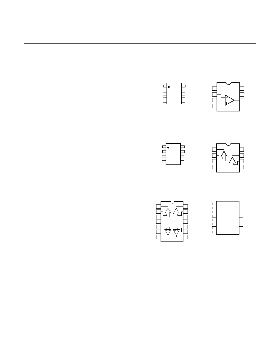
14-Lead Epoxy DIP
(P Suffix)
16-Lead Wide Body SOL
(S Suffix)
8-Lead Epoxy DIP
(P Suffix)
8-Lead SO
(S Suffix)
8-Lead Epoxy DIP
(P Suffix)
8-Lead SO
(S Suffix)
1
2
3
4
8
7
6
5
OP293
OUT B
≠IN B
+IN B
V+
OUT A
≠IN A
+IN A
V≠
OP293
OUT A
≠IN A
+IN A
V≠
OUT B
≠IN B
+IN B
V+
NC = NO CONNECT
1
2
3
4
8
7
6
5
OUT A
V+
NULL
NC
NULL
≠IN A
+IN A
V≠
OP193
OP193
OUT A
V+
NULL
NC
NULL
≠IN A
+IN A
V≠
14
13
12
11
10
9
8
1
2
3
4
5
6
7
OP493
OUT A
≠IN A
+IN A
V+
+IN B
≠IN B
OUT B
OUT D
≠IN D
+IN D
V≠
+IN C
≠IN C
OUT C
OP493
OUT D
≠IN D
+IN D
V≠
+IN C
≠IN C
OUT C
NC
OUT A
≠IN A
+IN A
V+
+IN B
≠IN B
OUT B
NC
NC = NO CONNECT

ELECTRICAL SPECIFICATIONS
"E" Grade
"F" Grade
Parameter
Symbol
Conditions
Min
Typ
Max
Min
Typ
Max
Units
INPUT CHARACTERISTICS
Offset Voltage
V
OS
OP193
75
150
µ
V
OP193, ≠40
∞
C
T
A
+125
∞
C
175
250
µ
V
OP293
100
250
µ
V
OP293, ≠40
∞
C
T
A
+125
∞
C
200
350
µ
V
OP493
125
275
µ
V
OP493, ≠40
∞
C
T
A
+125
∞
C
225
375
µ
V
Input Bias Current
I
B
V
CM
= 0 V,
≠40
∞
C
T
A
+125
∞
C
15
20
nA
Input Offset Current
I
OS
V
CM
= 0 V,
≠40
∞
C
T
A
+125
∞
C
2
4
nA
Input Voltage Range
V
CM
≠14.9
+13.5
≠14.9
+13.5
V
Common-Mode Rejection
CMRR
≠14.9
V
CM
+14 V
100
116
97
116
dB
≠14.9
V
CM
+14 V,
≠40
∞
C
T
A
+125
∞
C
97
94
dB
Large Signal Voltage Gain
A
VO
R
L
= 100 k
,
≠10 V
V
OUT
+10 V
500
500
V/mV
≠40
∞
C
T
A
+85
∞
C
300
300
V/mV
≠40
∞
C
T
A
+125
∞
C
300
300
V/mV
Large Signal Voltage Gain
A
VO
R
L
= 10 k
,
≠10 V
V
OUT
+10 V
350
350
V/mV
≠40
∞
C
T
A
+85
∞
C
200
200
V/mV
≠40
∞
C
T
A
+125
∞
C
150
150
V/mV
Large Signal Voltage Gain
A
VO
R
L
= 2 k
,
≠10 V
V
OUT
+10 V
200
200
V/mV
≠40
∞
C
T
A
+85
∞
C
125
125
V/mV
≠40
∞
C
T
A
+125
∞
C
100
100
V/mV
Long Term Offset Voltage
V
OS
Note 1
150
300
µ
V
Offset Voltage Drift
V
OS
/
T
Note 2
0.2
1.75
µ
V/
∞
C
OUTPUT CHARACTERISTICS
Output Voltage Swing High
V
OH
I
L
= 1 mA
+14.1 14.2
+14.1 14.2
V
I
L
= 1 mA,
≠40
∞
C
T
A
+125
∞
C
+14.0
+14.0
V
I
L
= 5 mA
+13.9 14.1
+13.9 14.1
V
Output Voltage Swing Low
V
OL
I
L
= ≠1 mA
≠14.7 ≠14.6
-14.7 ≠14.6
V
I
L
= ≠1 mA,
≠40
∞
C
T
A
+125
∞
C
≠14.4
≠14.4
V
I
L
= ≠5 mA
14.2 ≠14.1
14.2 ≠14.1
V
Short Circuit Current
I
SC
±
25
±
25
mA
POWER SUPPLY
Power Supply Rejection Ratio
PSRR
V
S
=
±
1.5 V to
±
18 V
100
120
97
120
dB
V
S
=
±
1.5 V to
±
18 V,
≠40
∞
C
T
A
+125
∞
C
97
94
dB
Supply Current/Amplifier
I
SY
≠40
∞
C
T
A
+125
∞
C, R
L
=
V
OUT
= 0 V, V
S
=
±
18 V
30
30
µ
A
NOISE PERFORMANCE
Voltage Noise Density
e
n
f = 1 kHz
65
65
nV/
Hz
Current Noise Density
i
n
f = 1 kHz
0.05
0.05
pA/
Hz
Voltage Noise
e
n
p-p
0.1 Hz to 10 Hz
3
3
µ
V p-p
DYNAMIC PERFORMANCE
Slew Rate
SR
R
L
= 2 k
15
15
V/ms
Gain Bandwidth Product
GBP
35
35
kHz
Channel Separation
V
OUT
= 10 V p-p,
R
L
= 2 k
, f = 1 kHz
120
120
dB
NOTES
1
Long term offset voltage is guaranteed by a 1000 hour life test performed on three independent lots at +125
∞
C, with an LTPD of 1.3.
2
Offset voltage drift is the average of the ≠40
∞
C to +25
∞
C delta and the +25
∞
C to +125
∞
C delta.
Specifications subject to change without notice.
OP193/OP293/OP493≠SPECIFICATIONS
REV. A
≠2≠
(@ V
S
= 15.0 V, T
A
= +25 C unless otherwise noted)

ELECTRICAL SPECIFICATIONS
"E" Grade
"F" Grade
Parameter
Symbol
Conditions
Min Typ
Max
Min Typ
Max
Units
INPUT CHARACTERISTICS
Offset Voltage
V
OS
OP193
75
150
µ
V
OP193, ≠40
∞
C
T
A
+125
∞
C
175
250
µ
V
OP293
100
250
µ
V
OP293, ≠40
∞
C
T
A
+125
∞
C
200
350
µ
V
OP493
125
275
µ
V
OP493, ≠40
∞
C
T
A
+125
∞
C
225
375
µ
V
Input Bias Current
I
B
≠40
∞
C
T
A
+125
∞
C
15
20
nA
Input Offset Current
I
OS
≠40
∞
C
T
A
+125
∞
C
2
4
nA
Input Voltage Range
V
CM
0
4
0
4
V
Common-Mode Rejection
CMRR
0.1
V
CM
+4 V
100
116
96
116
dB
0.1
V
CM
+4 V,
≠40
∞
C
T
A
+125
∞
C
92
92
dB
Large Signal Voltage Gain
A
VO
R
L
= 100 k
,
0.03
V
OUT
+4.0 V
200
200
V/mV
≠40
∞
C
T
A
+85
∞
C
125
125
V/mV
≠40
∞
C
T
A
+125
∞
C
130
130
V/mV
Large Signal Voltage Gain
A
VO
R
L
= 10 k
,
0.03
V
OUT
+4.0 V
75
75
V/mV
≠40
∞
C
T
A
+85
∞
C
50
50
V/mV
≠40
∞
C
T
A
+125
∞
C
70
70
V/mV
Long Term Offset Voltage
V
OS
Note 1
150
300
µ
V
Offset Voltage Drift
V
OS
/
T
Note 2
0.2
1.25
µ
V/
∞
C
OUTPUT CHARACTERISTICS
Output Voltage Swing High
V
OH
I
L
= 100
µ
A
4.4
4.4
V
I
L
= 1 mA
+4.1 4.4
+4.1 4.4
V
I
L
= 1 mA,
≠40
∞
C
T
A
+125
∞
C
+4.0
+4.0
V
I
L
= 5 mA
+4.0 4.4
+4.0 4.4
V
Output Voltage Swing Low
V
OL
I
L
= ≠100
µ
A
140
160
140
160
mV
I
L
= ≠100
µ
A,
≠40
∞
C
T
A
+125
∞
C
220
220
mV
No Load
5
5
mV
I
L
= ≠1 mA
280
400
280
400
mV
I
L
= ≠1 mA,
≠40
∞
C
T
A
+125
∞
C
500
500
mV
I
L
= ≠5 mA
700
900
700
900
mV
Short Circuit Current
I
SC
±
8
±
8
mA
POWER SUPPLY
Power Supply Rejection Ratio
PSRR
V
S
=
±
1.7 V to
±
6.0 V
100
120
97
120
dB
V
S
=
±
1.5 V to
±
18 V,
≠40
∞
C
T
A
+125
∞
C
94
90
dB
Supply Current/Amplifier
I
SY
V
CM
= 2.5 V, R
L
=
14.5
14.5
µ
A
NOISE PERFORMANCE
Voltage Noise Density
e
n
f = 1 kHz
65
65
nV/
Hz
Current Noise Density
i
n
f = 1 kHz
0.05
0.05
pA/
Hz
Voltage Noise
e
n
p-p
0.1 Hz to 10 Hz
3
3
µ
V p-p
DYNAMIC PERFORMANCE
Slew Rate
SR
R
L
= 2 k
12
12
V/ms
Gain Bandwidth Product
GBP
35
35
kHz
NOTES
1
Long term offset voltage is guaranteed by a 1000 hour life test performed on three independent lots at +125
∞
C, with an LTPD of 1.3.
2
Offset voltage drift is the average of the ≠40
∞
C to +25
∞
C delta and the +25
∞
C to +125
∞
C delta.
Specifications subject to change without notice.
REV. A
≠3≠
(@ V
S
= +5.0 V, V
CM
= 0.1 V, T
A
= +25 C unless otherwise noted)
OP193/OP293/OP493

REV. A
≠4≠
OP193/OP293/OP493
ELECTRICAL SPECIFICATIONS
"E" Grade
"F" Grade
Parameter
Symbol
Conditions
Min Typ
Max
Min Typ
Max
Units
INPUT CHARACTERISTICS
Offset Voltage
V
OS
OP193
75
150
µ
V
OP193, ≠40
∞
C
T
A
+125
∞
C
175
250
µ
V
OP293
100
250
µ
V
OP293, ≠40
∞
C
T
A
+125
∞
C
200
350
µ
V
OP493
125
275
µ
V
OP493, ≠40
∞
C
T
A
+125
∞
C
225
375
µ
V
Input Bias Current
I
B
≠40
∞
C
T
A
+125
∞
C
15
20
nA
Input Offset Current
I
OS
≠40
∞
C
T
A
+125
∞
C
2
4
nA
Input Voltage Range
V
CM
0
2
0
2
V
Common-Mode Rejection
CMRR
0.1
V
CM
+2 V
97
116
94
116
dB
0.1
V
CM
+2 V,
≠40
∞
C
T
A
+125
∞
C
90
87
dB
Large Signal Voltage Gain
A
VO
R
L
= 100 k
, 0.03
V
OUT
2 V
100
100
V/mV
≠40
∞
C
T
A
+85
∞
C
75
75
V/mV
≠40
∞
C
T
A
+125
∞
C
100
100
V/mV
Long Term Offset Voltage
V
OS
Note 1
150
300
µ
V
Offset Voltage Drift
V
OS
/
T
Note 2
0.2
1.25
µ
V/
∞
C
OUTPUT CHARACTERISTICS
Output Voltage Swing High
V
OH
I
L
= 1 mA
+2.1 2.14
+2.1 2.14
V
I
L
= 1 mA,
≠40
∞
C
T
A
+125
∞
C
1.9
1.9
V
I
L
= 5 mA
+1.9 2.1
+1.9 2.1
V
Output Voltage Swing Low
V
OL
I
L
= ≠1 mA
280
400
280
400
mV
I
L
= ≠1 mA
≠40
∞
C
T
A
+125
∞
C
500
500
mV
I
L
= ≠5 mA
700
900
700
900
mV
Short Circuit Current
I
SC
±
8
±
8
mA
POWER SUPPLY
Power Supply Rejection Ratio
PSRR
V
S
= +1.7 V to +6 V,
100
97
≠40
∞
C
T
A
+125
∞
C
94
90
dB
Supply Current/Amplifier
I
SY
V
CM
= 1.5 V, R
L
=
14.5 22
14.5 22
µ
A
≠40
∞
C
T
A
+125
∞
C
22
22
µ
A
Supply Voltage Range
V
S
+2
±
18
+2
±
18
V
NOISE PERFORMANCE
Voltage Noise Density
e
n
f = 1 kHz
65
65
nV/
Hz
Current Noise Density
i
n
f = 1 kHz
0.05
0.05
pA/
Hz
Voltage Noise
e
n
p-p
0.1 Hz to 10 Hz
3
3
µ
V p-p
DYNAMIC PERFORMANCE
Slew Rate
SR
R
L
= 2 k
10
10
V/ms
Gain Bandwidth Product
GBP
25
25
kHz
Channel Separation
V
OUT
= 10 V p-p,
R
L
= 2 k
, f = 1 kHz
120
120
dB
NOTES
1
Long term offset voltage is guaranteed by a 1000 hour life test performed on three independent lots at +125
∞
C, with an LTPD of 1.3.
2
Offset voltage drift is the average of the ≠40
∞
C to +25
∞
C delta and the +25
∞
C to +125
∞
C delta.
Specifications subject to change without notice.
(@ V
S
= +3.0 V, V
CM
= 0.1 V, T
A
= +25 C unless otherwise noted)

ELECTRICAL SPECIFICATIONS
"E" Grade
"F" Grade
Parameter
Symbol
Conditions
Min Typ
Max
Min Typ
Max
Units
INPUT CHARACTERISTICS
Offset Voltage
V
OS
OP193
75
150
µ
V
OP193, ≠40
∞
C
T
A
+125
∞
C
175
250
µ
V
OP293
100
250
µ
V
OP293, ≠40
∞
C
T
A
+125
∞
C
175
350
µ
V
OP493
125
275
µ
V
OP493, ≠40
∞
C
T
A
+125
∞
C
225
375
µ
V
Input Bias Current
I
B
≠40
∞
C
T
A
+125
∞
C
15
20
nA
Input Offset Current
I
OS
≠40
∞
C
T
A
+125
∞
C
2
4
nA
Input Voltage Range
V
CM
0
1
0
1
V
Large Signal Voltage Gain
A
VO
R
L
= 100 k
, 0.03
V
OUT
1 V
60
60
V/mV
≠40
∞
C
T
A
+125
∞
C
70
70
V/mV
Long Term Offset Voltage
V
OS
Note 1
150
300
µ
V
POWER SUPPLY
Power Supply Rejection Ratio
PSRR
V
S
= +1.7 V to +6 V,
100
97
≠40
∞
C
T
A
+125
∞
C
94
90
dB
Supply Current/Amplifier
I
SY
V
CM
= 1.0 V, R
L
=
13.2 20
13.2 20
µ
A
≠40
∞
C
T
A
+125
∞
C
25
25
µ
A
Supply Voltage Range
V
S
+2
±
18
+2
±
18
V
NOISE PERFORMANCE
Voltage Noise Density
e
n
f = 1 kHz
65
65
nV/
Hz
Current Noise Density
i
n
f = 1 kHz
0.05
0.05
pA/
Hz
Voltage Noise
e
n
p-p
0.1 Hz to 10 Hz
3
3
µ
V p-p
DYNAMIC PERFORMANCE
Slew Rate
SR
R
L
= 2 k
10
10
V/ms
Gain Bandwidth Product
GBP
25
25
kHz
WAFER TEST LIMITS
Parameter
Symbol
Conditions
Limit
Units
Offset Voltage
V
OS
V
S
=
±
15 V, V
OUT
= 0 V
±
75
µ
V max
V
S
= +2 V, V
OUT
= 1.0 V
±
75
µ
V max
Input Bias Current
I
B
V
CM
= 1.0 V
20
nA max
Input Offset Current
I
OS
V
CM
= 1.0 V
4
nA max
Input Voltage Range
1
V
CM
0 to 4
V min
Common-Mode Rejection
CMRR
0
V
CM
4 V
96
dB min
Power Supply Rejection Ratio
PSRR
V
S
=
±
1.5 V to
±
18 V
100
dB min
Large Signal Voltage Gain
A
VO
R
L
= 100 k
100
V/mV min
Output Voltage Swing High
V
OH
I
L
= 1 mA
4.1
V min
Output Voltage Swing Low
V
OL
I
L
= ≠1 mA
400
mV max
Supply Current/Amplifier
I
SY
V
O
= 0 V, R
L
=
, V
S
=
±
18 V
25
µ
A max
NOTES
Electrical tests and wafer probe to the limits shown. Due to variations in assembly methods and normal yield loss, yield after packaging is not guaranteed for standard
product dice. Consult factory to negotiate specifications based on dice lot qualifications through sample lot assembly and testing.
1
Guaranteed by CMRR test.
Specifications subject to change without notice.
(@ V
S
= +2.0 V, V
CM
= 0.1 V, T
A
= +25 C unless otherwise noted)
OP193/OP293/OP493
REV. A
≠5≠
(@ V
S
= +5.0 V, V
CM
= 0.1 V, V
OUT
= 2 V, T
A
= +25 C unless otherwise noted)
REV. A
≠6≠
OP193/OP293/OP493
ABSOLUTE MAXIMUM RATINGS
1
Supply Voltage . . . . . . . . . . . . . . . . . . . . . . . . . . . . . . . .
±
18 V
Input Voltage
2
. . . . . . . . . . . . . . . . . . . . . . . . . . . . . . . .
±
18 V
Differential Input Voltage
2
. . . . . . . . . . . . . . . . . . . . . . .
±
18 V
Output Short-Circuit Duration to Gnd . . . . . . . . . . Indefinite
Storage Temperature Range
P, S Package . . . . . . . . . . . . . . . . . . . . . . . ≠65
∞
C to +150
∞
C
Operating Temperature Range
OP193/OP293/OP493E, F . . . . . . . . . . . . ≠40
∞
C to +125
∞
C
Junction Temperature Range
P, S Package . . . . . . . . . . . . . . . . . . . . . . . ≠65
∞
C to +150
∞
C
Lead Temperature Range (Soldering, 60 sec) . . . . . . . +300
∞
C
Package Type
JA
3
JC
Units
8-Pin Plastic DIP (P)
103
43
∞
C/W
8-Pin SOIC (S)
158
43
∞
C/W
14-Pin Plastic DIP (P)
83
39
∞
C/W
16-Pin SOL (S)
92
27
∞
C/W
NOTES
1
Absolute maximum ratings apply to both DICE and packaged parts, unless
otherwise noted.
2
For supply voltages less than
±
18 V, the input voltage is limited to the supply
voltage.
3
JA
is specified for the worst case conditions, i.e.,
JA
is specified for device in socket
for P-DIP, and
JA
is specified for device soldered in circuit board for SOIC
package.
WARNING!
ESD SENSITIVE DEVICE
CAUTION
ESD (electrostatic discharge) sensitive device. Electrostatic charges as high as 4000 V readily
accumulate on the human body and test equipment and can discharge without detection.
Although the OP193/OP293/OP493 feature proprietary ESD protection circuitry, permanent
damage may occur on devices subjected to high energy electrostatic discharges. Therefore,
proper ESD precautions are recommended to avoid performance degradation or loss of
functionality.
ORDERING GUIDE
Temperature
Package
Package
Model
Range
Description
Option
OP193EP
≠40
∞
C to +125
∞
C
8-Pin Plastic DIP
N-8
OP193ES
≠40
∞
C to +125
∞
C
8-Pin SOIC
SO-8
OP193ES-REEL
≠40
∞
C to +125
∞
C
8-Pin SOIC
SO-8
OP193ES-REEL7
≠40
∞
C to +125
∞
C
8-Pin SOIC
SO-8
OP193FP
≠40
∞
C to +125
∞
C
8-Pin Plastic DIP
N-8
OP193FS
≠40
∞
C to +125
∞
C
8-Pin SOIC
SO-8
OP193FS-REEL
≠40
∞
C to +125
∞
C
8-Pin SOIC
SO-8
OP193FS-REEL7
≠40
∞
C to +125
∞
C
8-Pin SOIC
SO-8
OP193GBC
+25
∞
C
DICE
OP293EP
≠40
∞
C to +125
∞
C
8-Pin Plastic DIP
N-8
OP293ES
≠40
∞
C to +125
∞
C
8-Pin SOIC
SO-8
OP293ES-REEL
≠40
∞
C to +125
∞
C
8-Pin SOIC
SO-8
OP293ES-REEL7
≠40
∞
C to +125
∞
C
8-Pin SOIC
SO-8
OP293FP
≠40
∞
C to +125
∞
C
8-Pin Plastic DIP
N-8
OP293FS
≠40
∞
C to +125
∞
C
8-Pin SOIC
SO-8
OP293FS-REEL
≠40
∞
C to +125
∞
C
8-Pin SOIC
SO-8
OP293FS-REEL7
≠40
∞
C to +125
∞
C
8-Pin SOIC
SO-8
OP293GBC
+25
∞
C
DICE
OP493EP
≠40
∞
C to +125
∞
C
14-Pin Plastic DIP
N-14
OP493ES
≠40
∞
C to +125
∞
C
16-Pin SOL
SOL-16
OP493ES-REEL
≠40
∞
C to +125
∞
C
16-Pin SOL
SOL-16
OP493FP
≠40
∞
C to +125
∞
C
14-Pin Plastic DIP
N-14
OP493FS
≠40
∞
C to +125
∞
C
16-Pin SOL
SOL-16
OP493FS-REEL
≠40
∞
C to +125
∞
C
16-Pin SOL
SOL-16
OP493GBC
+25
∞
C
DICE
DICE CHARACTERISTICS
2
1
3
4
6
5
8
7
OP493 Die Size 0.106
◊
0.143 Inch, 15,158 Sq. Mils Substrate
(Die Backside) Is Connected to V≠ Transistor Count, 215
2
1
3
4
6
5
7
OP193 Die Size 0.070
◊
0.055 Inch, 3,850 Sq. Mils Substrate
(Die Backside) Is Connected to V≠ Transistor Count, 55
2
1
3
4
6
5
8
7
OP293 Die Size 0.072
◊
0.110 Inch, 7,920 Sq. Mils Substrate
(Die Backside) Is Connected to V≠ Transistor Count, 105
Typical Performance Characteristics≠OP193/OP293/OP493
REV. A
≠7≠
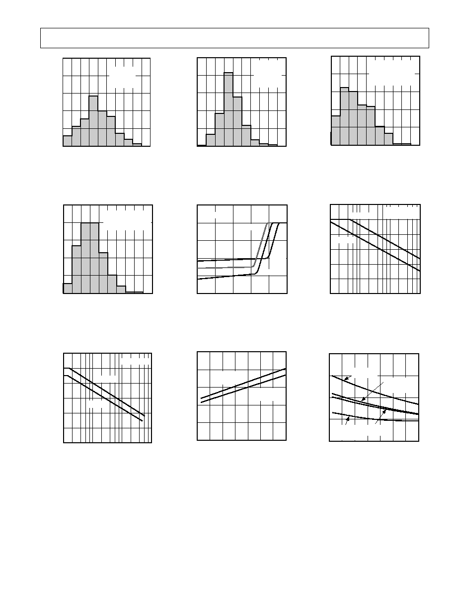
120
NUMBER OF AMPLIFIERS
40
≠75
75
0
80
OFFSET ≠ µV
160
≠45
60
45
≠30
0
30
V
S
= +3V
V
CM
= 0.1V
T
A
= +25
∞
C
450 x PDIPS
200
15
≠15
≠60
Figure 2. OP193 Offset Distribution,
V
S
= +3 V
INPUT BIAS CURRENT ≠ nA
5
≠2
0
≠1
≠3
COMMON MODE VOLTAGE ≠ Volts
0
1
2
3
4
1
≠4
+125
∞
C
≠40
∞
C
V
S
= +5V
+25
∞
C
Figure 5. Input Bias Current vs.
Common-Mode Voltage
75
15
SLEW RATE ≠ V/ms
5
≠50
0
10
20
≠25
125
0
25
50
100
+SR = ≠SR
V
S
=
±
15V
25
+SR = ≠SR
V
S
= +5V
TEMPERATURE ≠
∞
C
Figure 8. Slew Rate vs. Temperature
V
S
=
±
15V
T
A
= +25
∞
C
450 x PDIPS
200
160
120
80
40
0
OFFSET ≠ µV
75
60
30
15
0
≠15
≠30
≠45
≠60
≠75
45
NUMBER OF AMPLIFIERS
Figure 1. OP193 Offset Distribution,
V
S
=
±
15 V
0.6
90
NUMBER OF AMPLIFIERS
30
0
1.0
0
60
TCV
OS
≠ µV/
∞
C
120
0.2
0.8
0.4
V
S
=
±
15V
≠40
∞
C
T
A
+125
∞
C
450 x PDIPS
150
Figure 4. OP193 TCV
OS
Distribution,
V
S
=
±
15 V
120
CMRR ≠ dB
100
80
40
60
20
0
V
S
= +5V
T
A
= +25
∞
C
V
S
=
±
15V
FREQUENCY ≠ Hz
10 100 1k 10k
Figure 7. CMRR vs. Frequency
V
S
= +3V
V
CM
= 0.1V
≠40
∞
C
T
A
+125
∞
C
450 x PDIPS
0.6
90
NUMBER OF AMPLIFIERS
30
0
1.0
0
60
TCV
OS
≠ µV/
∞
C
120
0.2
0.8
0.4
150
Figure 3. OP193 TCV
OS
Distribution,
V
S
= +3 V
100
80
40
10 100 1k 10k
FREQUENCY ≠ Hz
60
20
0
PSRR ≠ dB
+PSRR
5V
V
S
30V
T
A
= +25
∞
C
≠PSRR
120
Figure 6. PSRR vs. Frequency
SHORT CIRCUIT CURRENT ≠ mA
|
≠ISC
|
V
S
=
±
15V
75
20
≠50
0
10
TEMPERATURE ≠
∞
C
30
≠25
125
0
25
50
100
40
+ISC
V
S
=
±
15V
|
≠ISC
|
V
S
= +5V
+ISC
V
S
= +5V
Figure 9. Short Circuit Current vs.
Temperature

REV. A
≠8≠
OP193/OP293/OP493≠Typical Performance Characteristics
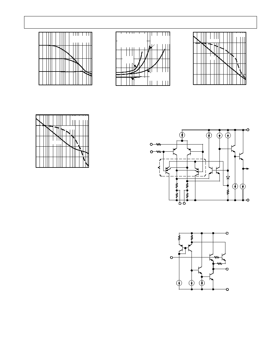
SUPPLY CURRENT ≠ µA
75
10
≠50
15
5
TEMPERATURE ≠
∞
C
20
≠25
125
0
25
50
100
25
V
S
= +2V
V
CM
= +1V
V
S
=
±
18V
0
Figure 12. Supply Current vs.
Temperature
10000
1000
10
0.1 1 10 100 1000 10000
100
1
DELTA FROM SUPPLY RAIL ≠ mV
5V
V
S
30V
T
A
= +25
∞
C
DELTA
FROM V
EE
DELTA
FROM V
CC
LOAD CURRENT ≠ µA
Figure 15. Delta Output Swing from
Either Rail vs. Current Load
GAIN ≠ dB
60
40
10 100 1k 10k 100k
0
≠20
T
A
= +25
∞
C
V
S
= +5V
FREQUENCY ≠ Hz
20
Figure 18. Closed-Loop Gain vs.
Frequency, V
S
= 5 V
INPUT OFFSET CURRENT ≠ nA
75
≠0.15
≠50
≠0.10
≠0.20
≠0.5
≠25
125
0
25
50
100
0
V
S
= +2V
V
CM
= 0.1V
V
S
=
±
15V
≠0.25
TEMPERATURE ≠
∞
C
Figure 10. Input Offset Current vs.
Temperature
1000
100
0.1 1 10 100 1k
10
1
5V
V
S
30V
T
A
= +25
∞
C
FREQUENCY ≠ Hz
VOLTAGE NOISE DENSITY ≠ nV/
Hz
Figure 13. Voltage Noise Density vs.
Frequency
VOLTAGE GAIN ≠ V/mV
75
1000
≠50
1500
500
2000
≠25
125
0
25
50
100
2500
V
S
=
±
15V
≠10V
V
OUT
+10V
0
V
S
= +5V
0.03V
V
OUT
4V
TEMPERATURE ≠
∞
C
Figure 16. Voltage Gain (R
L
= 100 k
)
vs. Temperature
INPUT BIAS CURRENT ≠ nA
75
≠3
≠50
≠2
≠4
TEMPERATURE ≠
∞
C
≠1
≠25
125
0
25
50
100
0
V
S
= +2V
V
CM
= 0.1V
V
S
=
±
15V
≠5
Figure 11. Input Bias Current vs.
Temperature
1000
100
0.1 1 10 100 1k
10
1
5V
V
S
30V
T
A
= +25
∞
C
FREQUENCY ≠ Hz
CURRENT NOISE DENSITY ≠ pA/
Hz
Figure 14. Current Noise Density vs.
Frequency
VOLTAGE GAIN ≠ V/mV
75
400
≠50
600
200
TEMPERATURE ≠
∞
C
800
≠25
125
0
25
50
100
1000
V
S
=
±
15V
≠10V
V
OUT
+10V
0
V
S
= +5V
0.03V
V
OUT
4V
Figure 17. Voltage Gain (R
L
= 10 k
)
vs. Temperature
OP193/OP293/OP493
REV. A
≠9≠
GAIN ≠ dB
60
40
10 100 1k 10k 100k
0
≠20
T
A
= +25
∞
C
V
S
=
±
15V
FREQUENCY ≠ Hz
20
Figure 19. Closed-Loop Gain vs.
Frequency, V
S
=
±
15 V
GAIN ≠ dB
60
40
100 1k 10k 100k 1M
0
≠20
V
S
=
±
15V
FREQUENCY ≠ Hz
20
PHASE
≠40
GAIN
PHASE ≠ Degrees
90
0
≠45
45
≠90
Figure 22. Open Loop, Gain and
Phase vs. Frequency
60
50
40
20
10 100 1000 10000
CAPACITIVE LOAD ≠ pF
30
10
0
OVERSHOOT ≠ %
V
S
= +5V T
A
= +25
∞
C
A
V
= 1
50mV
V
IN
150mV
LOADS TO GND
+OS
R
L
=
+OS =
|
≠OS
|
R
L
= 10k
+OS = |
≠OS
|
R
L
= 50k
≠OS
R
L
=
Figure 20. Small Signal Overshoot
vs. Capacitive Load
GAIN ≠ dB
60
40
100 1k 10k 100k 1M
0
≠20
V
S
= +5V
FREQUENCY ≠ Hz
20
PHASE
≠40
GAIN
PHASE ≠ Degrees
90
0
≠45
45
≠90
Figure 21. Open Loop, Gain and
Phase vs. Frequency
FUNCTIONAL DESCRIPTION
The OP193 family of operational amplifiers are single-supply,
micropower, precision amplifiers whose input and output ranges
both include ground. Input offset voltage (V
OS
) is only 75
µ
V
maximum, while the output will deliver
±
5 mA to a load. Sup-
ply current is only 17
µ
A.
A simplified schematic of the input stage is shown in Figure 23.
Input transistors Q1 and Q2 are PNP devices, which permit the
inputs to operate down to ground potential. The input transis-
tors have resistors in series with the base terminals to protect the
junctions from over voltage conditions. The second stage is an
NPN cascode which is buffered by an emitter follower before
driving the final PNP gain stage.
The OP193 includes connections to taps on the input load resis-
tors, which can be used to null the input offset voltage, V
OS
.
The OP293 and OP493 have two additional transistors, Q7 and
Q8. The behavior of these transistors is discussed in the Output
Phase Reversal section of this data sheet.
The output stage, shown in Figure 24, is a noninverting NPN
"totem-pole" configuration. Current is sourced to the load by
emitter follower Q1, while Q2 provides current sink capability.
When Q2 saturates, the output is pulled to within 5 mV of
ground without an external pull-down resistor. The totem-pole
output stage will supply a minimum of 5 mA to an external
load, even when operating from a single 3.0 V power supply.
By operating as an emitter follower, Q1 offers a high impedance
load to the final PNP collector of the input stage. Base drive to
Q2 is derived by monitoring Q1's collector current. Transistor
Q5 tracks the collector current of Q1. When Q1 is on, Q5 keeps
Q4 off, and current source I1 keeps Q2 turned off. When Q1 is
driven to cutoff (i.e., the output must move toward V≠), Q5
allows Q4 to turn on. Q4's collector current then provides the
base drive for Q3 and Q2, and the output low voltage swing is
set by Q2's V
CE,SAT
which is about 5 mV.
2k
NULLING
TERMINALS
(OP193 ONLY)
+INPUT
R2
A
2k
≠INPUT
Q1
Q2
Q7
Q8
Q3
Q4
R2
B
R1
B
R1
A
OP293,
OP493
ONLY
I
1
D1
I
2
I
3
I
4
Q5
Q6
TO
OUTPUT
STAGE
I
5
I
6
V≠
V+
Figure 23. OP193/OP293/OP493 Equivalent Input Circuit
Q4
Q1
Q5
Q3
Q2
OUTPUT
I
1
I
2
I
3
FROM
INPUT
STAGE
V+
V≠
Figure 24. OP193/OP293/OP493 Equivalent Output Circuit
REV. A
≠10≠
OP193/OP293/OP493
Driving Capacitive Loads
OP193 family amplifiers are unconditionally stable with capaci-
tive loads less than 200 pF. However, the small signal, unity-
gain overshoot will improve if a resistive load is added. For
example, transient overshoot is 20% when driving a 1000 pF/
10 k
load. When driving large capacitive loads in unity-gain
configurations, an in-the-loop compensation technique is rec-
ommended as illustrated in Figure 28.
Input Overvoltage Protection
As previously mentioned, the OP193 family of op amps use a
PNP input stage with protection resistors in series with the
inverting and noninverting inputs. The high breakdown of the
PNP transistors, coupled with the protection resistors, provides
a large amount of input protection from over voltage conditions.
The inputs can therefore be taken 20 V beyond either supply
without damaging the amplifier.
Output Phase Reversal--OP193
The OP193's input PNP collector-base junction can be forward-
biased if the inputs are brought more than one diode drop
(0.7 V) below ground. When this happens to the noninverting
input, Q4 of the cascode stage turns on and the output goes
high. If the positive input signal can go below ground, phase
reversal can be prevented by clamping the input to the negative
supply (i.e., GND) with a diode. The reverse leakage of the
diode will, of course, add to the input bias current of the ampli-
fier. If input bias current is not critical, a 1N914 will add less
than 10 nA of leakage. However, its leakage current will double
for every 10
∞
C increase in ambient temperature. For critical
applications, the collector-base junction of a 2N3906 transistor
will only add about 10 pA of additional bias current. To limit
the current through the diode under fault conditions, a 1 k
resistor is recommended in series with the input. (The OP193's
internal current limiting resistors will not protect the external
diode).
Output Phase Reversal--OP293 and OP493
The OP293 and OP493 include lateral PNP transistors Q7 and
Q8 to protect against phase reversal. If an input is brought more
than one diode drop (
0.7 V) below ground, Q7 and Q8 com-
bine to level shift the entire cascode stage, including the bias to
Q3 and Q4, simultaneously. In this case Q4 will not saturate
and the output remains low.
The OP293 and OP493 do not exhibit output phase reversal for
inputs up to ≠5 V below V≠ at +25
∞
C. The phase reversal limit
at +125
∞
C is about ≠3 V. If the inputs can be driven below these
levels, an external clamp diode, as discussed in the previous sec-
tion, should be added.
Battery Powered Applications
OP193 series op amps can be operated on a minimum supply
voltage of +1.7 V, and draw only 13
µ
A of supply current per
amplifier from a 2.0 V supply. In many battery-powered cir-
cuits, OP193 devices can be continuously operated for thou-
sands of hours before requiring battery replacement, thus
reducing equipment downtime and operating cost.
High performance portable equipment and instruments fre-
quently use lithium cells because of their long shelf life, light
weight, and high energy density relative to older primary cells.
Most lithium cells have a nominal output voltage of 3 V and are
noted for a flat discharge characteristic. The low supply voltage
requirement of the OP193, combined with the flat discharge
characteristic of the lithium cell, indicates that the OP193 can
be operated over the entire useful life of the cell. Figure 25
shows the typical discharge characteristic of a 1 AH lithium cell
powering the OP193, OP293, and OP493, with each amplifier,
in turn, driving 2.1 Volts into a 100 k
load.
LITHIUM SULPHUR DIOXIDE
CELL VOLTAGE ≠ Volts
5000
0
2
1
HOURS
3
1000
7000
2000
3000
4000
6000
4
0
OP493
OP293
OP193
Figure 25. Lithium Sulfur Dioxide Cell Discharge Charac-
teristic with OP193 Family and 100 k
Loads
Input Offset Voltage Nulling
The OP193 provides two offset nulling terminals that can be
used to adjust the OP193's internal V
OS
. In general, operational
amplifier terminals should never be used to adjust system offset
voltages. The offset null circuit of Figure 26 provides about
±
7 mV of offset adjustment range. A 100 k
resistor placed in
series with the wiper arm of the offset null potentiometer, as
shown in Figure 27, reduces the offset adjustment range to
400
µ
V and is recommended for applications requiring high null
resolution. Offset nulling does not adversely affect TCV
OS
per-
formance, providing that the trimming potentiometer tempera-
ture coefficient does not exceed
±
100 ppm/
∞
C.
6
5
7
4
1
2
3
V≠
V+
OP193
100k
Figure 26. Offset Nulling Circuit

OP193/OP293/OP493
REV. A
≠11≠
6
5
7
4
1
2
3
V≠
V+
OP193
100k
100k
Figure 27. High Resolution Offset Nulling Circuit
A Micropower False-Ground Generator
Some single supply circuits work best when inputs are biased
above ground, typically at 1/2 of the supply voltage. In these
cases a false ground can be created by using a voltage divider
buffered by an amplifier. One such circuit is shown in Figure 28.
This circuit will generate a false-ground reference at 1/2 of the
supply voltage, while drawing only about 27
µ
A from a 5 V sup-
ply. The circuit includes compensation to allow for a 1
µ
F by-
pass capacitor at the false-ground output. The benefit of a large
capacitor is that not only does the false ground present a very
low dc resistance to the load, but its ac impedance is low as well.
The OP193 can both sink and source more than 5 mA, which
improves recovery time from transients in the load current.
6
7
2
3
10k
OP193
100
4
+5V OR +12V
0.022µF
1µF
240k
240k
1µF
+2.5V OR +6V
Figure 28. A Micropower False-Ground Generator
A Battery Powered Voltage Reference
The circuit of Figure 29 is a battery-powered voltage reference
that draws only 17
µ
A of supply current. At this level, two AA
alkaline cells can power this reference for more than 18 months.
At an output voltage of 1.23 V @ 25
∞
C, drift of the reference is
only 5.5
µ
V/
∞
C over the industrial temperature range. Load
regulation is 85
µ
V/mA with line regulation at 120
µ
V/V.
Design of the reference is based on the Brokaw bandgap core
technique. Scaling of resistors R1 and R2 produces unequal cur-
rents in Q1 and Q2. The resulting
V
BE
across R3 creates a tem-
perature-proportional voltage (PTAT) which, in turn, produces
a larger temperature-proportional voltage across R4 and R5, V1.
The temperature coefficient of V1 cancels (first order) the
complementary to absolute temperature (CTAT) coefficient of
V
BE1
. When adjusted to 1.23 V @ +25
∞
C, output voltage
tempco is at a minimum. Bandgap references can have start-up
problems. With no current in R1 and R2, the OP193 is beyond
its positive input range limit and has an undefined output state.
Shorting Pin 5 (an offset adjust pin) to ground forces the output
high under these circumstances and insures reliable startup
without significantly degrading the OP193's offset drift.
6
7
2
3
C1
1000pF
OP193
V
BE2
4
R2
1.5M
Q1
V
OUT
(1.23V @ 25
∞
C)
5
R1
240k
V+
(+2.5V TO +36V)
Q2
1
2
3
7
6
5
V
BE1
MAT-01AH
V
BE
R3 68k
R5 20k
OUTPUT
ADJUST
R4
130k
V1
Figure 29. A Battery Powered Voltage Reference
A Single-Supply Current Monitor
Current monitoring essentially consists of amplifying the voltage
drop across a resistor placed in series with the current to be
measured. The difficulty is that only small voltage drops can be
tolerated, and with low precision op amps this greatly limits the
overall resolution. The single-supply current monitor of Figure
30 has a resolution of 10
µ
A and is capable of monitoring 30
mA of current. This range can be adjusted by changing the cur-
rent sense resistor R1. When measuring total system current, it
may be necessary to include the supply current of the current
monitor, which bypasses the current sense resistor, in the final
result. This current can be measured and calibrated (together
with the residual offset) by adjustment of the offset trim potenti-
ometer, R2. This produces a deliberate temperature dependent
offset. However, the supply current of the OP193 is also propor-
tional to temperature, and the two effects tend to track. Current
in R4 and R5, which also bypasses R1, can be adjusted via a
gain trim.
6
7
2
3
OP193
4
R2
100k
V
OUT =
100mV/mA(I
TEST
)
5
V+
1
R2
9.9k
R3
100k
R5
100
R1
1
TO CIRCUIT
UNDER TEST
I
TEST
Figure 30. Single-Supply Current Monitor
REV. A
≠12≠
OP193/OP293/OP493
A Single-Supply Instrumentation Amplifier
Designing a true single-supply instrumentation amplifier with
zero-input and zero-output operation requires special care. The
traditional configuration, shown in Figure 31, depends upon
amplifier A1's output being at 0 V when the applied common-
mode input voltage is at 0 V. Any error at the output is multi-
plied by the gain of A2. In addition, current flows through
resistor R3 as A2's output voltage increases. A1's output must
remain at 0 V while sinking the current through R3, or a gain
error will result. With a maximum output voltage of 4 V, the
current through R3 is only 2
µ
A, but this will still produce an
appreciable error.
+5V
V+
V≠
+5V
V+
V≠
V
OUT
R4
1.98M
R3
20k
R2
1.98M
R1
20k
I
S I N K
≠IN
+IN
1/2 OP293
A2
1/2 OP293
A1
Figure 31. A Conventional Instrumentation Amplifier
One solution to this problem is to use a pull-down resistor. For
example, if R3 = 20 k
, then the pull-down resistor must be
less than 400
. However, the pull-down resistor appears as a
fixed load when a common-mode voltage is applied. With a 4 V
common-mode voltage, the additional load current will be 10 mA,
which is unacceptable in a low power application.
Figure 32 shows a better solution. A1's sink current is provided
by a pair of N-channel FET transistors, configured as a current
mirror. With the values shown, sink current of Q2 is about
340
µ
A. Thus, with a common-mode voltage of 4 V, the addi-
tional load current is limited to 340
µ
A versus 10 mA with a
400
resistor.
+5V
V+
V≠
+5V
V+
V≠
V
OUT
+IN
1/2 OP293
A2
R4
1.98M
R3
20k
R2
1.98M
R1
20k
≠IN
1/2 OP293
A1
+5V
10k
Q1
Q2
VN2222
Figure 32. An Improved Single-Supply, 0 V
IN
, 0 V
OUT
Instrumentation Amplifier
A Low-Power, Temperature to 4≠20 mA Transmitter
A simple temperature to 4≠20 mA transmitter is shown in Fig-
ure 33. After calibration, this transmitter is accurate to
±
0.5
∞
C
over the ≠50
∞
C to +150
∞
C temperature range. The transmitter
operates from +8 V to +40 V with supply rejection better than
3 ppm/V. One half of the OP293 is used to buffer the V
TEMP
pin, while the other half regulates the output current to satisfy
the current summation at its noninverting input:
I
OUT
+
V
TEMP
◊
R6
+
R7
(
)
R2
◊
R10
≠ V
SET
R2
+
R6
+
R7
R2
◊
R10
The change in output current with temperature is the derivative
of the transfer function:
I
OUT
T
=
V
TEMP
T
( R6
+
R7)
R2
◊
R10
SPAN TRIM
8
4
+8V TO +40V
V+
1/2 OP293
R4
20k
R9
100k
R2
1k
1/2 OP293
V
TEMP
2N1711
1
2
3
R1 10k
2
6
3
4
REF-43BZ
V
I N
V
OUT
V
TEMP
GND
R5
5k
R3
100k
6
5
ZERO
TRIM
V
SET
7
R6
3k
R7
5k
R8
1k
1N4002
R10
100
1%, 1/2 W
R
LOAD
I
OUT
ALL RESISTORS 1/4W, 5% UNLESS OTHERWISE NOTED
Figure 33. Temperature to 4≠20 mA Transmitter

OP193/OP293/OP493
REV. A
≠13≠
From the formulas, it can be seen that if the span trim is ad-
justed before the zero trim, the two trims are not interactive,
which greatly simplifies the calibration procedure.
Calibration of the transmitter is simple. First, the slope of the
output current versus temperature is calibrated by adjusting the
span trim, R7. A couple of iterations may be required to be sure
the slope is correct.
Once the span trim has been completed, the zero trim can be
made. Remember that adjusting the zero trim will not affect the
gain.
The zero trim can be set at any known temperature by adjusting
R5 until the output current equals:
I
OUT
=
I
FS
T
OPERATING
(T
AMBIENT
-
T
MIN
)
+
4 mA
Table I shows the values of R6 required for various temperature
ranges.
Table I. R6 Values vs. Temperature
Temp Range
R6
0
∞
C to +70
∞
C
10 k
≠40
∞
C to +85
∞
C
6.2 k
≠55
∞
C to +150
∞
C
3 k
A Micropower Voltage Controlled Oscillator
An OP293 in combination with an inexpensive quad CMOS
analog switch forms the precision VCO of Figure 34. This cir-
cuit provides triangle and square wave outputs and draws only
50
µ
A from a single 5 V supply. A1 acts as an integrator; S1
switches the charging current symmetrically to yield positive and
negative ramps. The integrator is bounded by A2 which acts as
a Schmitt trigger with a precise hysteresis of 1.67 volts, set by
resistors R5, R6, and R7, and associated CMOS switches. The
resulting output of A1 is a triangle wave with upper and lower
levels of 3.33 and 1.67 volts. The output of A2 is a square wave
with almost rail-to-rail swing. With the components shown, fre-
quency of operation is given by the equation:
f
OUT
= V
CONTROL
(Volts)
◊
10 Hz/V
but this can easily be changed by varying C1. The circuit oper-
ates well up to 500 Hz.
8
4
1/2 OP293
1
2
3
R3
100k
V
CONTROL
R4
200k
TRIANGLE
OUT
A1
+5V
R1
200k
R2
200k
1/2 OP293
6
5
7
A2
SQUARE
OUT
+5V
R6
200k
R7
200k
S3
S4
S1
1 IN/OUT
2 OUT/IN
CONT 12
OUT/IN 10
3 OUT/IN
S2
CONT 13
4 IN/OUT
6 CONT
5 CONT
7
V
SS
IN/OUT 8
IN/OUT 11
OUT/IN 9
V
DD
14
+5V
+5V
CD4066
R8
200k
+5V
R5
200k
C1
75nF
Figure 34. Micropower Voltage Controlled Oscillator
A Micropower, Single-Supply Quad Voltage Output 8-Bit
DAC
The circuit of Figure 35 uses the DAC8408 CMOS quad 8-bit
DAC and the OP493 to form a single-supply quad voltage out-
put DAC with a supply drain of only 140
µ
A. The DAC8408 is
used in the voltage switching mode and each DAC has an out-
put resistance (
10 k
) independent of the digital input code.
The output amplifiers act as buffers to avoid loading the DACs.
The 100 k
resistors ensure that the OP493 outputs will swing
to within 1/2 LSB of ground, i.e.:
1
2
◊
1.23 V
256
=
3 mV
REV. A
≠14≠
OP193/OP293/OP493
V
OUT
A
1/4 OP493
A
2
3
R1
100k
11
1
2
V
REF
A
I
OUT1A
I
OUT1B
4
5
6
I
OUT2A/2B
DAC A
1/4
DAC8408
DAC B
1/4
DAC8408
I
OUT1C
DAC C
1/4
DAC8408
I
OUT1D
DAC D
1/4
DAC8408
V
OUT
B
1/4 OP493
B
6
5
R2
100k
7
8
V
REF
B
V
OUT
C
1/4 OP493
C
13
12
R3
100k
14
27
V
REF
C
V
OUT
D
1/4 OP493
D
9
10
R4
100k
8
21
V
REF
D
DAC DATA BUS
PINS 9(LSB)≠16(MSB)
24 I
OUT2C/2D
23
25
+5V
1
V
DD
AD589
1.23V
+5V
17
18
19
20
A/B
R/W
DS1
DS2
DAC8408ET
DIGITAL
CONTROL
SIGNALS
28
DGND
OP493
4
+5V
3.6k
Figure 35. Micropower Single-Supply Quad Voltage-
Output 8-Bit DAC
A Single-Supply Micropower Quad Programmable-Gain
Amplifier
The combination of the quad OP493 and the DAC8408 quad
8-bit CMOS DAC creates a quad programmable gain amplifier
with a quiescent supply drain of only 140
µ
A (Figure 36). The
digital code present at the DAC, which is easily set by a micro-
processor, determines the ratio between the fixed DAC feedback
resistor and the resistance that the DAC feedback ladder pre-
sents to the op amp feedback loop. The gain of each amplifier is:
V
OUT
V
IN
=
256
n
where n equals the decimal equivalent of the 8-bit digital code
present at the DAC.
If the digital code present at the DAC consists of all zeros, the
feedback loop will be open causing the op amp to saturate. The
10 M
resistors placed in parallel with the DAC feedback loop
eliminates this problem with a very small reduction in gain accu-
racy. The 2.5 V reference biases the amplifiers to the center of
the linear region providing maximum output swing.

OP193/OP293/OP493
REV. A
≠15≠
7
R
FB
B
C2
0.1µF
V
I N
B
3
R
FB
A
C1
0.1µF
V
IN
A
V
OUT
A
1/4 OP493
A
2
3
11
1
4
V
REF
A
I
OUT2A/2B
1
DAC A
1/4
DAC8408
DAC B
1/4
DAC8408
DAC D
1/4
DAC8408
V
OUT
B
1/4 OP493
B
5
7
8
V
REF
B
V
OUT
C
9
8
25
V
OUT
D
12
14
OP493
13
R4
10M
23
I
OUT1D
DAC DATA BUS
PINS 9(LSB)≠16(MSB)
22
R
FB
D
C4
0.1µF
V
I N
D
+5V
17
18
19
20
A/B
R/W
DS1
DS2
DAC8408ET
DIGITAL
CONTROL
SIGNALS
28
DGND
4
+2.5V
REFERENCE
VOLTAGE
I
OUT1C
I
OUT2C/2D
V
REF
D
21
24
R3
10M
1/4 OP493
C
10
26
R
FB
C
C3
0.1µF
V
I N
C
DAC C
1/4
DAC8408
R2
10M
27
I
OUT1B
V
REF
C
I
OUT1A
R1
10M
6
V
DD
2
1/4 OP493
D
6
5
Figure 36. Single-Supply Micropower Quad Programmable-Gain Amplifier
REV. A
≠16≠
OP193/OP293/OP493
OUTLINE DIMENSIONS
Dimensions shown in inches and (mm).
8-Lead SO
(S Suffix)
8-Lead Epoxy DIP
(P Suffix)
0.0098 (0.25)
0.0075 (0.19)
0.0500 (1.27)
0.0160 (0.41)
8
∞
0
∞
0.0196 (0.50)
0.0099 (0.25)
x 45
∞
PIN 1
0.1574 (4.00)
0.1497 (3.80)
0.2440 (6.20)
0.2284 (5.80)
4
5
1
8
0.0192 (0.49)
0.0138 (0.35)
0.0500
(1.27)
BSC
0.0688 (1.75)
0.0532 (1.35)
0.0098 (0.25)
0.0040 (0.10)
0.1968 (5.00)
0.1890 (4.80)
PIN 1
0.280 (7.11)
0.240 (6.10)
4
5
8
1
SEATING
PLANE
0.060 (1.52)
0.015 (0.38)
0.130
(3.30)
MIN
0.210
(5.33)
MAX
0.160 (4.06)
0.115 (2.93)
0.430 (10.92)
0.348 (8.84)
0.022 (0.558)
0.014 (0.356)
0.070 (1.77)
0.045 (1.15)
0.100
(2.54)
BSC
0.325 (8.25)
0.300 (7.62)
0.015 (0.381)
0.008 (0.204)
0.195 (4.95)
0.115 (2.93)
16-Lead Wide Body SOL
(S Suffix)
PIN 1
0.2992 (7.60)
0.2914 (7.40)
0.4193 (10.65)
0.3937 (10.00)
1
16
9
8
0.0192 (0.49)
0.0138 (0.35)
0.0500 (1.27)
BSC
0.1043 (2.65)
0.0926 (2.35)
0.4133 (10.50)
0.3977 (10.00)
0.0118 (0.30)
0.0040 (0.10)
0.0125 (0.32)
0.0091 (0.23)
0.0500 (1.27)
0.0157 (0.40)
8
∞
0
∞
0.0291 (0.74)
0.0098 (0.25)
x 45
∞
14-Lead Epoxy DIP
(P Suffix)
0.325 (8.25)
0.300 (7.62)
0.015 (0.381)
0.008 (0.204)
0.195 (4.95)
0.115 (2.93)
0.210
(5.33)
MAX
0.160 (4.06)
0.115 (2.93)
0.795 (20.19)
0.725 (18.42)
0.022 (0.558)
0.014 (0.356)
0.100
(2.54)
BSC
0.070 (1.77)
0.045 (1.15)
SEATING
PLANE
0.060 (1.52)
0.015 (0.38)
0.130
(3.30)
MIN
PIN 1
0.280 (7.11)
0.240 (6.10)
7
8
14
1
PRINTED IN U.S.A.
C1994≠18≠1/95