 | –≠–ª–µ–∫—Ç—Ä–æ–Ω–Ω—ã–π –∫–æ–º–ø–æ–Ω–µ–Ω—Ç: OP297 | –°–∫–∞—á–∞—Ç—å:  PDF PDF  ZIP ZIP |
Document Outline
- Specifications
- Pinout
- Package drawings
- Ordering Guide
- Features
- Applications
- Product Description
- Absolute Maximum Ratings
- Typical Characteristics
- Wafer Test Limits
- DICE CHARACTERISTICS
- DIAGRAMS
- Channel Separation Test Circuit
- Guard Ring Layout and Connections
- Precision Absolute Value Amplifier
- Precision Current Pump
- Precision Positive Peak Detector
- A Simple Bridge Conditioning Amplifier Using the OP297
- Squaring Amplifier
- Square-Root Amplifier
- OP297 Macro-Model

8/21/97 4:00 PM
REV. D
Information furnished by Analog Devices is believed to be accurate and
reliable. However, no responsibility is assumed by Analog Devices for its
use, nor for any infringements of patents or other rights of third parties
which may result from its use. No license is granted by implication or
otherwise under any patent or patent rights of Analog Devices.
a
OP297
One Technology Way, P.O. Box 9106, Norwood, MA 02062-9106, U.S.A.
Tel: 617/329-4700
World Wide Web Site: http://www.analog.com
Fax: 617/326-8703
© Analog Devices, Inc., 1997
Dual Low Bias Current
Precision Operational Amplifier
PIN CONNECTIONS
Plastic Epoxy-DIP (P Suffix)
8-Pin Cerdip (Z Suffix)
8-Pin Narrow Body SOIC (S Suffix)
FEATURES
Precision Performance in Standard SO-8 Pinout
Low Offset Voltage: 50 V max
Low Offset Voltage Drift: 0.6 V/ C max
Very Low Bias Current:
+25 C (100 pA max)
≠55 C to +125 C (450 pA max)
Very High Open-Loop Gain (2000 V/mV min)
Low Supply Current (Per Amplifier): 625 A max
Operates From 62 V to 620 V Supplies
High Common-Mode Rejection: 120 dB min
Pin Compatible to LT1013, AD706, AD708, OP221,
LM158, and MC1458/1558 with Improved Performance
APPLICATIONS
Strain Gauge and Bridge Amplifiers
High Stability Thermocouple Amplifiers
Instrumentation Amplifiers
Photo-Current Monitors
High-Gain Linearity Amplifiers
Long-Term Integrators/Filters
Sample-and-Hold Amplifiers
Peak Detectors
Logarithmic Amplifiers
Battery-Powered Systems
GENERAL DESCRIPTION
The OP297 is the first dual op amp to pack precision perfor-
mance into the space-saving, industry standard 8-pin SO pack-
age. Its combination of precision with low power and extremely
low input bias current makes the dual OP297 useful in a wide
variety of applications.
Precision performance of the OP297 includes very low offset,
under 50
µ
V, and low drift, below 0.6
µ
V/
∞
C. Open-loop gain
exceeds 2000 V/mV insuring high linearity in every application.
Errors due to common-mode signals are eliminated by the
OP297's common-mode rejection of over 120 dB. The
OP297's power supply rejection of over 120 dB minimizes
offset voltage changes experienced in battery powered systems.
Supply current of the OP297 is under 625
µ
A per amplifier and
it can operate with supply voltages as low as
±
2 V.
The OP297 utilizes a super-beta input stage with bias current
cancellation to maintain picoamp bias currents at all tempera-
tures. This is in contrast to FET input op amps whose bias
currents start in the picoamp range at 25
∞
C, but double for
every 10
∞
C rise in temperature, to reach the nanoamp range
above 85
∞
C. Input bias current of the OP 297 is under 100 pA
at 25
∞
C and is under 450 pA over the military temperature
range.
Combining precision, low power and low bias current, the
OP297 is ideal for a number of applications including instru-
mentation amplifiers, log amplifiers, photodiode preamplifiers
and long-term integrators. For a single device, see the OP97;
for a quad, see the OP497.
Figure 1. Low Bias Current Over Temperature
Figure 2. Very Low Offset
1
2
3
4
5
6
7
8
OUT A
V+
≠IN A
OUT B
+IN A
≠IN B
V≠
+IN B
+
≠
+
≠
B
A
TEMPERATURE (
∞
C)
INPUT
CURRENT
(pA)
6 0
4 0
2 0
0
2 0
≠ 4 0
≠ 6 0
≠75 ≠50 ≠25
0
25
50
75
100 125
V
S
=
±
15V
V
CM
= 0V
I
B
≠
I
B
+
I
OS
INPUT OFFSET VOLTAGE (
µ
V)
NUMBER OF UNITS
400
300
200
100
0
≠100 ≠80 ≠60 ≠40 ≠20 0
20
40 60 80 100
1200 UNITS
T
A
= +25
∞
C
V
S
=
±
15V
V
CM
= 0V
8/21/97 4:00 PM
≠2≠
REV. D
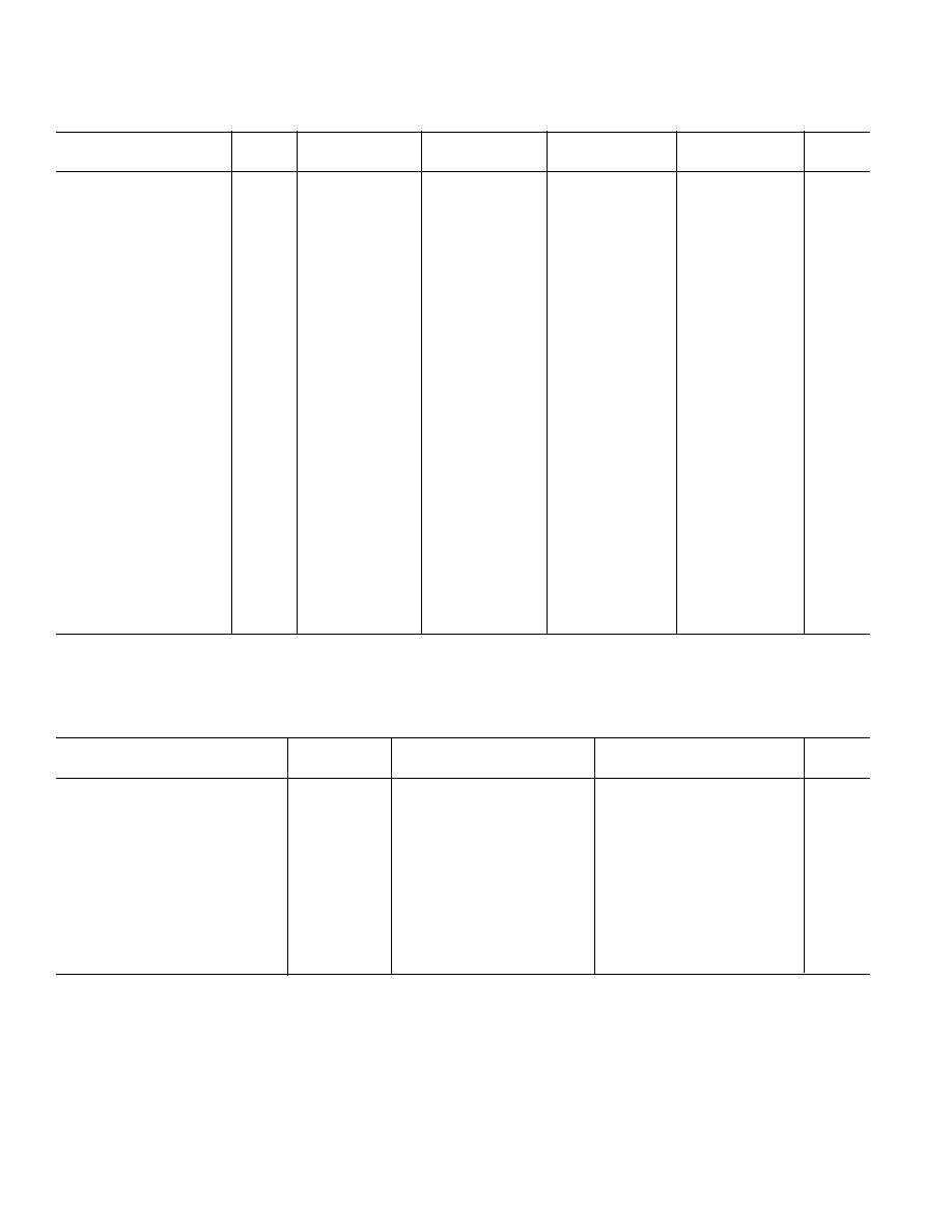
OP297≠SPECIFICATIONS
ELECTRICAL CHARACTERISTICS
OP297A/E
OP297F
OP297G
Parameter
Symbol
Conditions
Min
Typ
Max
Min
Typ
Max
Min
Typ
Max
Units
Input Offset Voltage
V
OS
25
50
50
100
80
200
µ
V
Long-Term Input
Voltage Stability
0.1
0.1
0.1
µ
V/mo
Input Offset Current
I
OS
V
CM
= 0 V
20
100
35
150
50
200
pA
Input Bias Current
I
B
V
CM
= 0 V
20
±
100
35
±
150
50
±
200
pA
Input Noise Voltage
e
n
p-p
0.1 Hz to 10 Hz
0.5
0.5
0.5
µ
V p-p
Input Noise
e
n
f
O
= 10 Hz
20
20
20
nV/
Hz
Voltage Density
e
n
f
O
= 1000 Hz
17
17
17
nV/
Hz
Input Noise Current Density
i
n
f
O
= 10 Hz
20
20
20
fA
Hz
Input Resistance
Differential Mode
R
IN
30
30
30
M
Input Resistance
Common-Mode
R
INCM
500
500
500
G
Large-Signal
V
O
=
±
10 V
Voltage Gain
A
VO
R
L
= 2 k
2000
4000
1500
3200
1200
3200
V/mV
Input Voltage Range
IVR
(Note 1)
±
13
±
14
±
13
±
14
±
13
±
14
V
Common-Mode Rejection
CMR
V
CM
=
±
13 V
120
140
114
135
114
135
dB
Power Supply Rejection
PSR
V
S
=
±
2 V to
±
20 V 120
130
114
125
114
125
dB
Output Voltage Swing
V
O
R
L
= 10 k
±
13
±
14
±
13
±
14
±
13
±
14
V
V
O
R
L
= 2 k
±
13
±
13.7
±
13
±
13.7
±
13
±
13.7
V
Supply Current Per Amplifier
I
SY
No Load
525
625
525
625
525
625
µ
A
Supply Voltage
V
S
Operating Range
±
2
±
20
±
2
±
20
±
2
±
20
V
Slew Rate
SR
0.05
0.15
0.05
0.15
0.05
0.15
V/
µ
s
Gain Bandwidth Product
GBWP
A
V
= +1
500
500
500
kHz
Channel Separation
CS
V
O
= 20 V p≠p
150
150
150
dB
f
O
= 10 Hz
Input Capacitance
C
IN
3
3
3
pF
NOTES
1
Guaranteed by CMR test.
Specifications subject to change without notice.
ELECTRICAL CHARACTERISTICS
OP297A
Parameter
Symbol
Conditions
Min
Typ
Max
Units
Input Offset Voltage
V
OS
45
100
µ
V
Average Input Offset Voltage Drift
TCV
OS
0.2
0.6
µ
V/
∞
C
Input Offset Current
I
OS
V
CM
= 0 V
60
450
pA
Input Bias Current
I
B
V
CM
= 0 V
60
±
450
pA
Large-Signal Voltage Gain
A
VO
V
O
=
±
10 V, R
L
= 2 k
1200
2700
V/mV
Input Voltage Range
IVR
(Note 1)
±
13
±
13.5
V
Common-Mode Rejection
CMR
V
CM
=
±
13
114
130
dB
Power Supply Rejection
PSR
V
S
=
±
2.5 V to
±
20 V
114
125
dB
Output Voltage Swing
V
O
R
L
= 10 k
±
13
±
13.4
V
Supply Current Per Amplifier
I
SY
No Load
575
750
µ
A
Supply Voltage
V
S
Operating Range
±
2.5
±
20
V
NOTES
1
Guaranteed by CMR test.
Specifications subject to change without notice.
(@ V
S
= 15 V, T
A
= +25 C, unless otherwise noted.)
(@ V
S
= 15 V, ≠55 C
T
A
+125 C for OP297A, unless otherwise noted.)

8/21/97 4:00 PM
≠3≠
REV. D
OP297
ELECTRICAL CHARACTERISTICS
OP297E
OP297F
OP297G
Parameter
Symbol
Conditions
Min
Typ
Max
Min
Typ
Max
Min
Typ
Max
Units
Input Offset Voltage
V
OS
35
100
80
300
110
400
µ
V
Average Input Offset
Voltage Drift
TCV
OS
0.2
0.6
0.5
2.0
0.6
2.0
µ
V/
∞
C
Input Offset Current
I
OS
V
CM
= 0 V
50
450
80
750
80
750
pA
Input Bias Current
I
B
V
CM
= 0 V
50
±
450
80
±
750
80
±
750
pA
Large-Signal Voltage Gain
A
VO
V
O
=
±
10 V,
R
L
= 2 k
1200
3200
1000
2500
700
2500
V/mV
Input Voltage Range
IVR
(Note 1)
±
13
±
13.5
±
13
±
13.5
±
13
±
13.5
V
Common-Mode Rejection
CMR
V
CM
=
±
13
114
130
108
130
108
130
dB
Power Supply Rejection
PSR
V
S
=
±
2.5 V
to
±
20 V
114
0.15
108
0.15
108
0.3
dB
Output Voltage Swing
V
O
R
L
= 10 k
±
13
±
13.4
±
13
±
13.4
±
13
±
13.4
V
Supply Current Per Amplifier I
SY
No Load
550
750
550
750
550
750
µ
A
Supply Voltage
V
S
Operating Range
±
2.5
±
20
±
2.5
±
20
±
2.5
±
20
V
NOTES
1
Guaranteed by CMR test.
Specifications subject to change without notice.
(@ V
S
= 15 V, ≠40 C
T
A
+85 C for OP297E/F/G, unless otherwise noted.)
Wafer Test Limits
Parameter
Symbol
Conditions
Limit
Units
Input Offset Voltage
V
OS
200
µ
V max
Input Offset Current
I
OS
V
CM
= 0 V
200
pA max
Input Bias Current
I
B
V
CM
= 0 V
±
200
pA max
Large-Signal Voltage Gain
A
VO
V
O
=
±
10 V, R
L
= 2 k
1200
V/mV min
Input Voltage Range
IVR
(Note 1)
±
13
V min
Common-Mode Rejection
CMR
V
CM
=
±
13 V
114
dB min
Power Supply
PSR
V
S
=
±
2 V to
±
l 8 V
114
dB min
Output Voltage Swing
V
O
R
L
= 2 k
±
13
V min
Supply Current Per Amplifier
I
SY
No Load
625
µ
A max
NOTES
1. Guaranteed by CMR test.
Electrical tests are performed at wafer probe to the limits shown. Due to variations in assembly methods and normal yield loss, yield after packaging is not guaranteed
for standard product dice. Consult factory to negotiate specifications based on dice lot qualifications through sample lot assembly and testing.
(@ V
S
= 15 V, T
A
= +25 C, unless otherwise noted.)
DICE CHARACTERISTICS
Dimension shown in inches and (mm).
Contact factory for latest dimensions
OUTPUT A
≠INPUT A
+INPUT A
≠V
S
0.074 (1.88)
+INPUT B
≠INPUT B
OUTPUT B
+V
S
0.118 (3.00)
8/21/97 4:00 PM
OP297
≠4≠
REV. D
WARNING!
ESD SENSITIVE DEVICE
CAUTION
ESD (electrostatic discharge) sensitive device. Electrostatic charges as high as 4000 V readily
accumulate on the human body and test equipment and can discharge without detection.
Although the OP297 features proprietary ESD protection circuitry, permanent damage may
occur on devices subjected to high energy electrostatic discharges. Therefore, proper ESD
precautions are recommended to avoid performance degradation or loss of functionality.
ABSOLUTE MAXIMUM RATINGS
1
Supply Voltage . . . . . . . . . . . . . . . . . . . . . . . . . . . . . . . .
±
20 V
Input Voltage
2
. . . . . . . . . . . . . . . . . . . . . . . . . . . . . . . .
±
20 V
Differential Input Voltage
2
. . . . . . . . . . . . . . . . . . . . . . . . 40 V
Output Short-Circuit Duration . . . . . . . . . . . . . . . . Indefinite
Storage Temperature Range
Z Package . . . . . . . . . . . . . . . . . . . . . . . . . ≠65
∞
C to +175
∞
C
P, S Package . . . . . . . . . . . . . . . . . . . . . . . ≠65
∞
C to +150
∞
C
Operating Temperature Range
OP297A (Z) . . . . . . . . . . . . . . . . . . . . . . . ≠55
∞
C to +125
∞
C
OP297E, F (Z) . . . . . . . . . . . . . . . . . . . . . . ≠40
∞
C to +85
∞
C
OP297F, G (P, S) . . . . . . . . . . . . . . . . . . . ≠40
∞
C to +85
∞
C
Junction Temperature
Z Package . . . . . . . . . . . . . . . . . . . . . . . . . ≠65
∞
C to +175
∞
C
P, S Package . . . . . . . . . . . . . . . . . . . . . . . ≠65
∞
C to +150
∞
C
Lead Temperature Range (Soldering, 60 sec) . . . . . . . +300
∞
C
Package Type
JA
3
JC
Units
8-Pin Cerdip (Z)
134
12
∞
C/W
8-Pin Plastic DIP (P)
96
37
∞
C/W
8-Pin SO (S)
150
41
∞
C/W
NOTES
1
Absolute maximum ratings apply to both DICE and packaged parts, unless
otherwise noted.
2
For supply voltages less than
±
20 V, the absolute maximum input voltage is equal
to the supply voltage.
3
JA
is specified for worst case mounting conditions, i.e.,
JA
is specified for device in
socket for cerdip and P-DIP, packages;
JA
is specified for device soldered to printed
circuit board for SO package.
ORDERING GUIDE
1
Temperature
Package
Package
Model
Range
Description
Option
1
OP297AZ
≠55
∞
C to +125
∞
C
8-Pin Cerdip
Q-8
OP297EZ
≠40
∞
C to +85
∞
C
8-Pin Cerdip
Q-8
OP297EP
≠40
∞
C to +85
∞
C
8-Pin Plastic DIP
N-8
OP297FP
≠40
∞
C to +85
∞
C
8-Pin Plastic DIP
N-8
OP297FS
≠40
∞
C to +85
∞
C
8-Pin SO
SO-8
OP297FS-REEL
≠40
∞
C to +85
∞
C
8-Pin SO
SO-8
OP297FS-REEL7
≠40
∞
C to +85
∞
C
8-Pin SO
SO-8
OP297GP
≠40
∞
C to +85
∞
C
8-Pin Plastic DIP
N-8
OP297GS
≠40
∞
C to +85
∞
C
8-Pin SO
SO-8
OP297GS-REEL
≠40
∞
C to +85
∞
C
8-Pin SO
SO-8
OP297GS-REEL7
2
≠40
∞
C to +85
∞
C
8-Pin SO
SO-8
NOTES
1
Burn-in is available on extended industrial temperature range parts in cerdip, and plastic DIP
packages. For outline information see Package Information section.
2
For availability and burn-in information on SO packages, contact your local sales office.
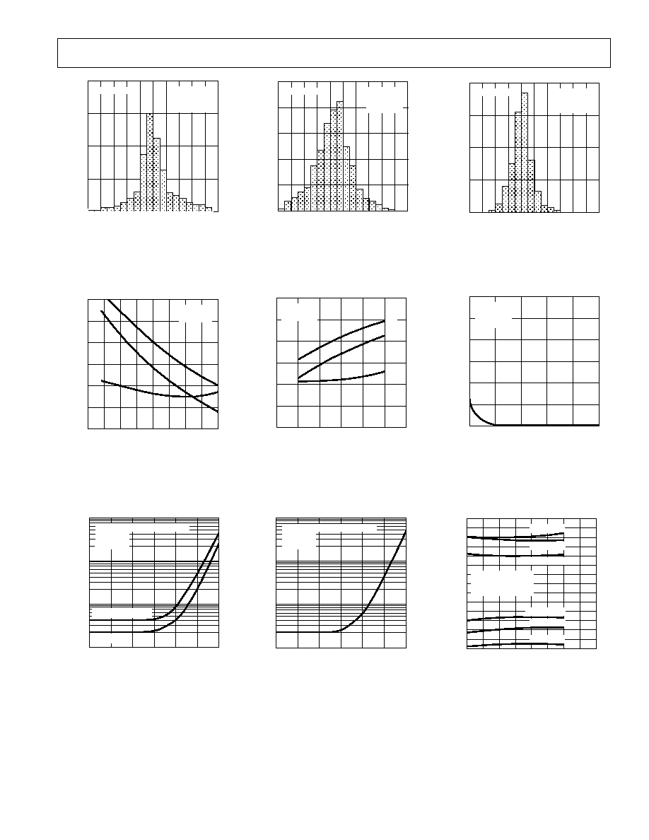
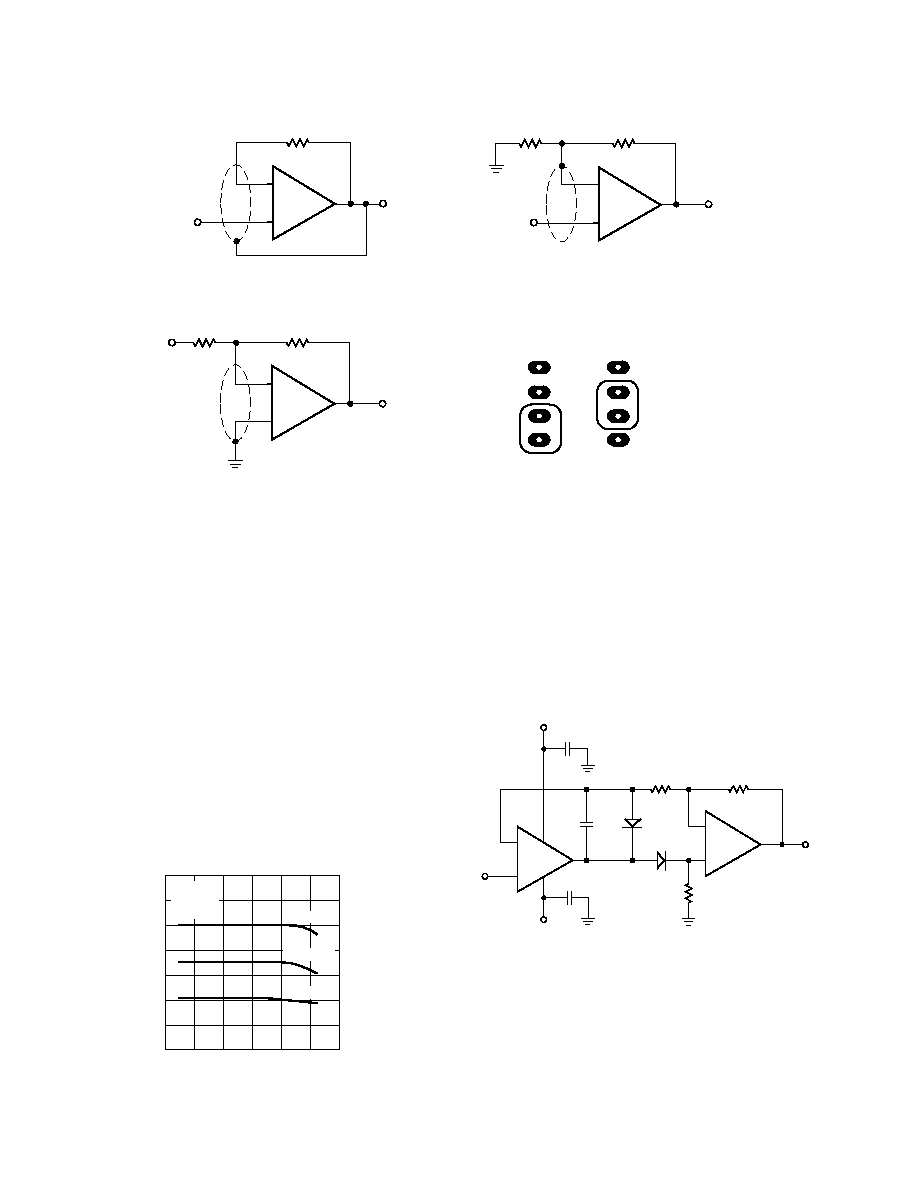
Figure 3. Channel Separation Test Circuit
+
≠
+
≠
V
1
20V
p-p
@ 10Hz
50
50k
V
2
CHANNEL SEPARATION = 20 log
1/2
OP-297
1/2
OP-297
2k
V
1
V
2
/10000
)
)
8/21/97 4:00 PM
OP297
≠5≠
REV. D
INPUT OFFSET VOLTAGE (
µ
V)
NUMBER OF UNITS
400
300
200
100
0
≠100 ≠80 ≠60 ≠40 ≠20 0
20
40 60 80 100
1200 UNITS
T
A
= +25
∞
C
V
S
=
±
15V
V
CM
= 0V
Figure 4. Typical Distribution of Input
Offset Voltage
TEMPERATURE (
∞
C)
INPUT
CURRENT
(pA)
6 0
4 0
2 0
0
2 0
≠ 4 0
≠ 6 0
≠75 ≠50 ≠25
0
25
50
75
100 125
V
S
=
±
15V
V
CM
= 0V
I
B
≠
I
B
+
I
OS
Figure 7. Input Bias, Offset Current
vs. Temperature
SOURCE RESISTANCE (
)
EFFECTIVE OFFSET
V
O
L
T
A
GE (
µ
V)
10
100
1k
10k
100k
1M
10M
10000
1000
100
10
BALANCED OR UNBALANCED
V
S
=
±
15V
V
CM
= 0V
≠55
∞
C
T
A
125
∞
C
T
A
= +25
∞
C
Figure 10. Effective Offset Voltage
vs. Source Resistance
Typical Performance Characteristics≠
INPUT BIAS CURRENT (pA)
NUMBER OF UNITS
≠100 ≠80 ≠60 ≠40 ≠20
0
20 40
60 80 100
250
200
150
100
50
0
1200
UNITS
T
A
= +25
∞
C
V
S
=
±
15V
V
CM
= 0V
Figure 5. Typical Distribution of Input
Bias Current
COMMON-MODE VOLTAGE (VOLTS)
INPUT
CURRENT
(pA)
60
40
20
0
≠20
≠40
≠60
≠15
≠10
≠5
0
5
10
15
T
A
= +25
∞
C
V
S
=
±
15V
I
B
≠
I
B
+
I
OS
Figure 8. Input Bias, Offset Current
vs. Common-Mode Voltage
SOURCE RESISTANCE (
)
EFFECTIVE OFFSET
V
O
L
T
A
GE DRIFT
(
µ
V/
∞
C)
100
100M
1k
10k
100k
1M
10M
100
10
1
0.1
BALANCED OR UNBALANCED
V
S
=
±
15V
V
CM
= 0V
Figure 11. Effective TCV
OS
vs. Source
Resistance
INPUT OFFSET CURRENT (pA)
NUMBER OF UNITS
400
300
200
100
0
≠100 ≠80 ≠60 ≠40 ≠20 0
20 40
60 80 100
1200 UNITS
T
A
= +25
∞
C
V
S
=
±
15V
V
CM
= 0V
Figure 6. Typical Distribution of In-
put Offset Current
TIME AFTER POWER APPLIED (MINUTES)
DEVIA
T
ION FR
OM FINAL
V
ALUE (
µ
V)
±
3
±
2
±
1
0
0
1
2
3
4
5
T
A
= +25
∞
C
V
S
=
±
15V
V
CM
= 0V
Figure 9. Input Offset Voltage Warm-
Up Drift
TIME FROM OUTPUT SHORT (MINUTES)
0
1
2
3
4
SHOR
T
-
CIRCUIT
CURRENT
(mA)
35
30
25
20
15
10
5
0
≠5
≠10
≠15
≠20
≠25
≠30
≠35
T
A
= ≠55
∞
C
T
A
= +25
∞
C
T
A
= +125
∞
C
V
S
=
±
15V
OUTPUT SHORTED
TO GROUND
T
A
= +125
∞
C
T
A
= +25
∞
C
T
A
= ≠55
∞
C
Figure 12. Short Circuit Current vs.
Time, Temperature
8/21/97 4:00 PM
OP297
≠6≠
REV. D
≠Typical Performance Characteristics
SUPPLY VOLTAGE (VOLTS)
T
O
T
A
L
SUPPL
Y
CURRENT
(
µ
A)
0
±
5
±
10
±
15
±
20
1300
1200
1100
1000
900
800
NO LOAD
T
A
= ≠55
∞
C
T
A
= +125
∞
C
T
A
= +25
∞
C
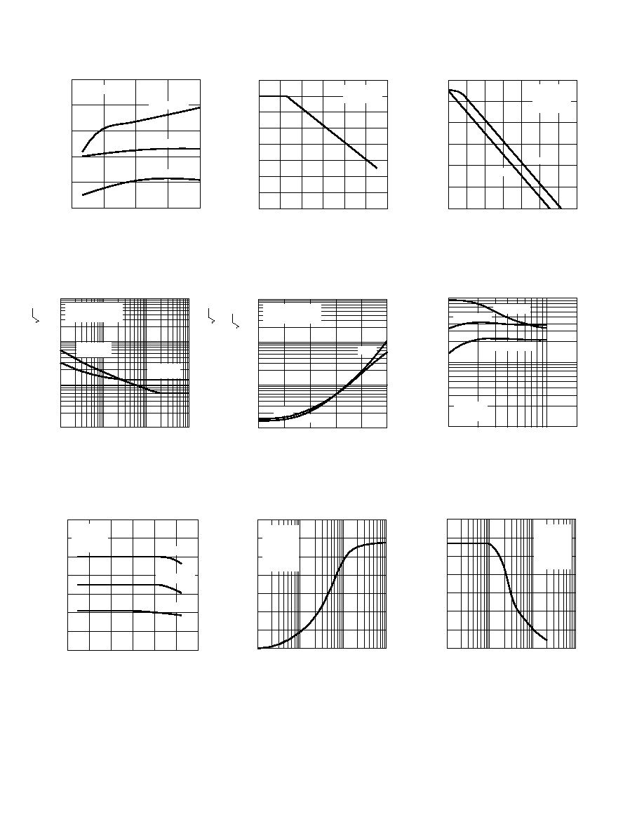
Figure 13. Total Supply Current vs.
Supply Voltage
T
A
= +25
∞
C
V
S
=
±
2V TO
±
15V
VOLTAGE
NOISE
V
O
L
T
A
GE NOISE DENSITY
(nV/ Hz)
CURRENT
NOISE DENSITY
(fA/ Hz)
FREQUENCY (Hz)
100
0
100
10
1
10
100
1000
1000
100
10
1
CURRENT
NOISE
Figure 16. Common-Mode Rejection
vs. Frequency
T
A
= +125
∞
C
T
A
= ≠55
∞
C
T
A
= +25
∞
C
R
L
= 10k
V
S
=
±
15V
V
CM
= 0V
OUTPUT VOLTAGE (VOLTS)
DIFFERENTIAL
INPUT
V
O
L
T
A
GE (10
µ
V/DIV)
≠15
≠10
≠5
0
5
10
15
Figure 19. Power Supply Rejection
vs. Frequency
FREQUENCY (Hz)
COMMON-MODE REJECTION (dB)
160
140
120
100
80
60
40
20
0
1
10
100
1k
10k
100k
1M
T
A
= +25
∞
C
V
S
=
±
15V
Figure 14. Noise Density vs.
Frequency
10
2
T
A
= +25
∞
C
V
S
=
±
2V TO
±
20V
10Hz
10Hz
10
3
10
4
10
5
10
6
10
7
SOURCE RESISTANCE (
)
1kHz
1kHz
T
O
T
A
L
NOISE DENSITY
(
µ
V/ Hz)
10
1
0.1
0.01
Figure 17. Total Noise Density vs.
Source Resistance
T
A
= +25
∞
C
V
S
=
±
15V
A
VCL
= +1
1%THD
fo = 1kHz
OUTPUT
SWING (V
p-p
)
35
30
25
20
15
10
5
0
LOAD RESISTANCE (
)
10
100
1k
10k
Figure 20. Open Loop Gain vs. Load
Resistance
+PSR
T
A
= +25
∞
C
V
S
=
±
15V
V
S
= 10V
p-p
≠PSR
PO
WER SUPPL
Y
REJECTION (dB)
140
120
100
80
60
40
20
FREQUENCY (Hz)
0.1
1
10
100
1k
10k
100k 1M
Figure 15. Open Loop Gain Linearity
T
A
= ≠55
∞
C
T
A
= +125
∞
C
T
A
= +25
∞
C
V
S
=
±
15V
V
O
=
±
10V
3
10000
1000
100
LOAD RESISTANCE (k
)
20
1
OPEN-LOOP
GAIN (V/mV)
2
5
10
Figure 18. Maximum Output Swing
vs. Load Resistance
Figure 21. Maximum Output Swing
vs. Frequency
T
A
= +25
∞
C
V
S
=
±
15V
A
VCL
= +1
1%THD
R
L
= 10k
35
30
25
20
15
10
5
0
OUTPUT
SWING (V
p-p
)
FREQUENCY (Hz)
100
1k
10k
100k

8/21/97 4:00 PM
OP297
≠7≠
REV. D
Figure 24. Open Loop Output
Impedance vs Frequency
APPLICATIONS INFORMATION
Extremely low bias current over the full military temperature
range makes the OP297 attractive for use in sample-and-hold
amplifiers, peak detectors, and log amplifiers that must operate
over a wide temperature range. Balancing input resistances is
not necessary with the OP297 Offset voltage and TCV
OS
are
degraded only minimally by high source resistance, even when
unbalanced.
The input pins of the OP297 are protected against large differ-
ential voltage by back-to-back diodes and current-limiting resis-
tors. Common-mode voltages at the inputs are not restricted,
and may vary over the full range of the supply voltages used.
The OP297 requires very little operating headroom about the
supply rails, and is specified for operation with supplies as low
as +2 V. Typically, the common-mode range extends to within
one volt of either rail. The output typically swings to within one
volt of the rails when using a 10 k
load.
AC PERFORMANCE
The OP297'S AC characteristics are highly stable over its full
operating temperature range. Unity-gain small-signal response is
shown in Figure 25. Extremely tolerant of capacitive loading on
the output, the OP297 displays excellent response even with
1000 pF loads (Figure 26).
10
0%
100
90
5µs
20mV
Figure 25. Small-Signal Transient Response
(C
LOAD
= 100 pF, A
VCL
= +1)
10
0%
100
90
5µs
20mV
Figure 26. Small-Signal Transient Response
(C
LOAD
= 1000 pF, A
VCL
= +1)
10
0%
100
90
5µs
20mV
Figure 27. Large-Signal Transient Response
(A
VCL
= +1)
GUARDING AND SHIELDING
To maintain the extremely high input impedances of the
OP297, care must be taken in circuit board layout and manu-
facturing. Board surfaces must be kept scrupulously clean and
free of moisture. Conformal coating is recommended to provide
T
A
= +125
∞
C
T
A
= ≠55
∞
C
GAIN
PHASE
V
S
=
±
15V
C
L
= 30pF
R
L
= 1M
FREQUENCY (Hz)
OPEN-LOOP
GAIN (dB)
100
80
60
40
20
0
≠20
≠40
100
1k
10k
100
1M
10M
90
135
180
225
PHASE SHIFT
(DEG)
+EDGE
≠EDGE
T
A
= +25
∞
C
V
S
=
±
15V
A
VCL
= +1
V
OUT
= 100mV
p-p
O
VERSHOO
T
(%)
70
60
50
40
30
20
10
0
LOAD CAPACITANCE (pF)
10
100
1000
10000
T
A
= +25
∞
C
V
S
=
±
15V
FREQUENCY (Hz)
OUTPUT
IMPED
ANCE (
)
1000
100
10
1
0.1
0.01
0.001
10
100
1k
10k
100k
1M
Figure 22. Open Loop Gain,
Phase vs. Frequency
Figure 23. Small Signal Overshoot
vs. Capacitance Load
8/21/97 4:00 PM
OP297
≠8≠
REV. D
a humidity barrier. Even a clean PC board can have 100 pA of
leakage currents between adjacent traces, so guard rings should
be used around the inputs. Guard traces are operated at a volt-
age close to that on the inputs, as shown in Figure 28, so that
leakage currents become minimal. In noninverting applications,
the guard ring should be connected to the common-mode volt-
age at the inverting input. In inverting applications, both inputs
remain at ground, so the guard trace should be grounded. Guard
traces should be on both sides of the circuit board.
OPEN-LOOP GAIN LINEARITY
The OP297 has both an extremely high gain of 2000 V/mV
minimum and constant gain linearity. This enhances the preci-
sion of the OP297 and provides for very high accuracy in high
closed loop gain applications. Figure 29 illustrates the typical
open-loop gain linearity of the OP297 over the military tempera-
ture range.
T
A
= +125
∞
C
T
A
= ≠55
∞
C
T
A
= +25
∞
C
R
L
= 10k
V
S
=
±
15V
V
CM
= 0V
OUTPUT VOLTAGE (VOLTS)
DIFFERENTIAL
INPUT
V
O
L
T
A
GE (10
µ
V/DIV)
≠15
≠10
≠5
0
5
10
15
Figure 29. Open-Loop Linearity of the OP297
APPLICATIONS
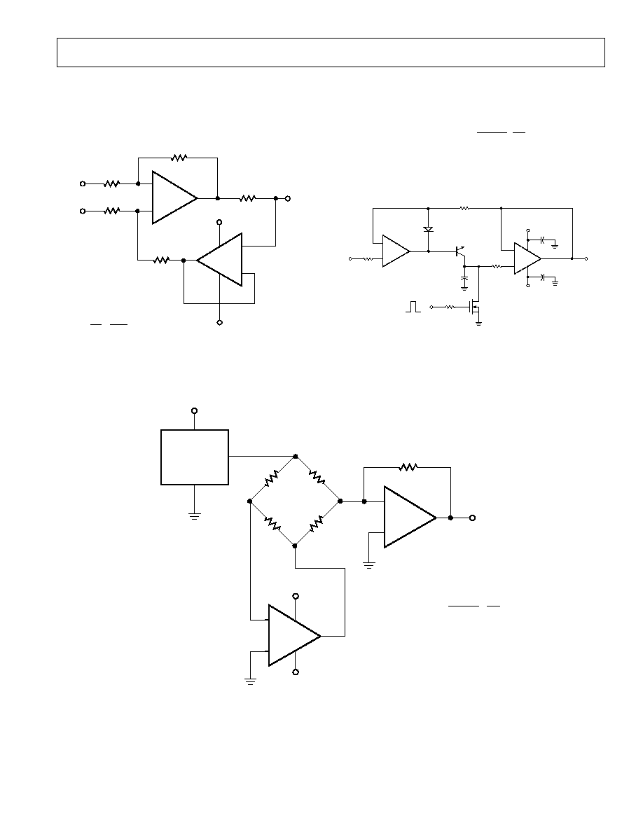
PRECISION ABSOLUTE VALUE AMPLIFIER
The circuit of Figure 30 is a precision absolute value amplifier
with an input impedance of 30 M
. The high gain and low
TCV
OS
of the OP297 insure accurate operation with microvolt
input signals. In this circuit, the input always appears as a
common-mode signal to the op amps. The CMR of the OP297
exceeds 120 dB, yielding an error of less than 2 ppm.
+
≠
0V < V
OUT
< 10V
7
6
5
R
3
1k
1/2
OP-297
R
2
2k
R
1
1k
D
1
1N4148
D
2
1N4148
+
≠
1/2
OP-297
C
1
30pF
≠15V
C
3
0.1
µ
F
4
1
8
2
3
V
IN
C
2
0.1
µ
F
+15V
Figure 30. Precision Absolute Value Amplifier
PRECISION CURRENT PUMP
Maximum output current of the precision current pump shown
in Figure 31 is
±
10 mA. Voltage compliance is
±
10 V with
±
15 V supplies. Output impedance of the current transmitter
exceeds 3 M
with linearity better than 16 bits.
≠
+
UNITY-GAIN FOLLOWER
INVERTING AMPLIFIER
NONINVERTING AMPLIFIER
1/2
OP-297
1/2
OP-297
≠
+
MINI-DIP
BOTTOM VIEW
1/2
OP-297
≠
+
1
8
B
A
Figure 28. Guard Ring Layout and Connections
8/21/97 4:00 PM
OP297
≠9≠
REV. D
PRECISION POSITIVE PEAK DETECTOR
In Figure 32, the C
H
must be of polystyrene, Teflon
Æ
*, or poly-
ethylene to minimize dielectric absorption and leakage. The
droop rate is determined by the size of C
H
and the bias current
of the OP297.
+
≠
V
IN
+
≠
≠
+
R
1
10k
R
2
10k
R
4
10k
1/2
OP-297
R
3
10k
2
3
1
R
5
100
I
OUT
±
10mA
+15V
5
6
4
8
7
≠15V
1/2
OP-297
I
OUT
=
V
IN
R
5
=
V
IN
100
= 10mA/V
Figure 31. Precision Current Pump
SIMPLE BRIDGE CONDITIONING AMPLIFIER
Figure 33 shows a simple bridge conditioning amplifier using
the OP297. The transfer function is:
V
OUT
=
V
REF
R
R
+
R
R
F
R
The REF43 provides an accurate and stable reference voltage
for the bridge. To maintain the highest circuit accuracy, R
F
should be 0.1% or better with a low temperature coefficient.
0.1
µ
F
0.1
µ
F
≠
+
1/2
OP-297
3
2
1
≠
+
5
6
8
7
4
+15V
≠15V
OUT
V
1k
IN
V
1N4148
2N930
1k
1k
RESET
H
C
1k
1/2
OP-297
Figure 32. Precision Positive Peak Detector
*Teflon is a registered trademark of the Dupont Company
Figure 33. A Simple Bridge Conditioning Amplifier Using the OP297
REF-43
R
R +
R
R
R
+5V
8
7
4
5
6
≠5V
1/2
OP-297
1/2
OP-297
2
1
3
V
OUT
R
F
+5V
2
6
V
REF
2.5V
4
≠
+
≠
+
V
OUT
V
REF
=
R
R +
R
R
F
R
(
(
8/21/97 4:00 PM
OP297
≠10≠
REV. D
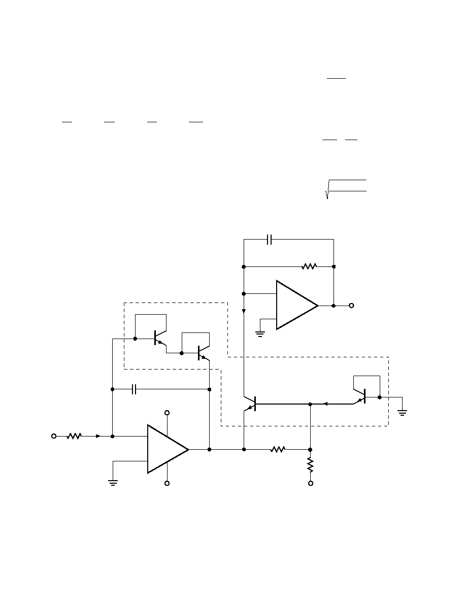
NONLINEAR CIRCUITS
Due to its low input bias currents, the OP297 is an ideal log
amplifier in nonlinear circuits such as the square and square-
root circuits shown in Figures 34 and 35. Using the squaring
circuit of Figure 34 as an example, the analysis begins by writing
a voltage loop equation across transistors Q
1
, Q
2
, Q
3
and Q
4
.
V
T1
ln
I
IN
I
S1
+
V
T 2
ln
I
IN
I
S2
=
V
T 3
ln
I
O
I
S3
+
V
T 4
ln
I
REF
I
S4
All the transistors of the MAT04 are precisely matched and at
the same temperature, so the I
S
and V
T
terms cancel, giving:
2 ln I
IN
= ln I
O
+ ln I
REF
= ln (I
O
◊
I
REF
)
Exponentiating both sides of the equation leads to:
I
O
=
(I
IN
)
2
I
REF
Op amp A
2
forms a current-to-voltage converter which gives
V
OUT
= R2
◊
10. Substituting (V
IN
/R1) for I
IN
and the above
equation for I
O
yields:
V
OUT
=
R2
I
REF
V
IN
R1
2
A similar analysis made for the square-root circuit of Figure 35
leads to its transfer function:
V
OUT
=
R2
(V
IN
)(I
REF
)
R1
Figure 34. Squaring Amplifier
V
IN
33k
1/2
OP-297
A
1
2
3
8
1
4
V≠
V+
C
1
100pF
C
2
100pF
R
2
33k
R
1
I
O
I
IN
I
REF
V
OUT
1/2
OP-297
A
2
6
5
7
MAT-04E
Q
1
1
3
2
Q
4
14
12
13
Q
2
7
5
6
Q
3
8
10
9
50k
R
3
50k
R
4
≠15V
≠
+
≠
+

8/21/97 4:00 PM
OP297
≠11≠
REV. D
In these circuits, I
REF
is a function of the negative power supply.
To maintain accuracy, the negative supply should be well regu-
lated. For applications where very high accuracy is required, a
voltage reference may be used to set I
REF
. An important consid-
eration for the squaring circuit is that a sufficiently large input
voltage can force the output beyond the operating range of the
output op amp. Resistor R4 can be changed to scale I
REF
, or R1,
and R2 can be varied to keep the output voltage within the
usable range.
Unadjusted accuracy of the square-root circuit is better than
0.1% over an input voltage range of 100 mV to 10 V. For a
similar input voltage range, the accuracy of the squaring circuit
is better than 0.5%.
Figure 35. Square-Root Amplifier
V
IN
33k
1/2
OP-297
2
3
8
1
4
V≠
V+
C
1
100pF
C
2
100pF
R
2
33k
R
1
I
O
I
IN
I
REF
V
OUT
1/2
OP-297
6
5
7
MAT-04E
Q
1
1
3
2
Q
4
14
12
13
Q
2
7
5
6
Q
3
8
10
9
2k
R
5
50k
R
3
50k
R
4
≠15V
≠
+
≠
+
OP297 SPICE MACRO-MODEL
Figures 36 and 37 show the node end net list for a SPICE
macro model of the OP297. The model is a simplified version of
the actual device and simulates important dc parameters such as
V
OS
, I
OS
, I
B
, A
VO
, CMR, V
O
and I
SY
. AC parameters such as
slew rate, gain and phase response and CMR change with fre-
quency are also simulated by the model.
The model uses typical parameters for the OP297. The poles
and zeros in the model were determined from the actual open
and closed-loop gain and phase response of the OP297. In this
way, the model presents an accurate ac representation of the
actual device. The model assumes an ambient temperature
of 25
∞
C.

8/21/97 4:00 PM
OP297
≠12≠
REV. D
Figure 36. OP297 Macro-Model
D
1
R
5
2
R
1
≠IN
+IN
1
I
OS
R
2
3
D
2
9
10
11
4
98
R
6
Q
2
Q
1
C
2
D
4
D
3
E
1
R
8
R
9
C
4
V
2
C
3
G
1
12
R
7
13
14
E
REF
50
I
1
R
3
R
4
5
6
15
16
C
IN
7
+≠
E
OS
R
IN1
R
IN2
8
99
V
3
≠
+
≠
+
≠
+
≠
+
98
C
8
G
3
22
R
15
E
3
R
13
R
14
C
7
C
5
E
2
R
11
R
12
G
2
17
R
10
C
6
≠
+
≠
+
99
D
10
22
26
27
28
29
25
L
1
50
+ ≠
≠ +
D
5
D
6
D
7
D
8
G
6
R
18
V
5
V
4
G
7
R
19
G
5
G
4
D
9
I
SY
R
16
23
R
17

8/21/97 4:00 PM
OP297
≠13≠
REV. D
OP297 SPICE MACRO-MODEL
∑
∑ NODE ASSIGNMENTS
∑NONINVERTING INPUT
INVERTING INPUT
OUTPUT
POSITIVE SUPPLY
NEGATIVE SUPPLY
∑
SUBCKT OP297
1 2
30 99 50
∑
INPUT STAGE & POLE AT 6 MHz
∑
RIN1
1
7
2500
RIN2
2
8
2500
R1
8
3
5E11
R2
7
3
5E11
R3
5
99
612
R4
6
99
612
CIN
7
8
3E-12
C2
5
6
21.67E-12
I1
4
50
0.1E-3
IOS
7
8
20E-12
EOS
9
7
POLY(1) 19
23
25E-6
1
Q1
5
8
10
QX
Q2
6
9
11
QX
R5
10
4
96
R6
11
4
96
D1
8
9
DX
D2
9
8
DX
∑
EREF 98
0
23
0
1
∑
GAIN STAGE & DOMINANT POLE AT 0.13 HZ
∑
R7
12
98
2.45E9
C3
12
98
500E-12
G1
98
12
5 6 1.634E-3
V2
99
13
1.5
V3
14
50
1.5
D3
12
13
DX
D4
14
12
DX
∑
∑ NEGATIVE ZERO AT -1 8 MHz
∑
R8
15
16
1E6
C4
15
16
≠88.4E-15
R9
16
98
1
E1
15
98
12
23
1E6
∑
Table I. SPICE Net-List
∑ POLE AT 1.8 MHz
∑
R10
17
98
1E6
C5
17
98
88 4E-15
G2
98
17
16 23 1 E-6
∑
∑ COMMON-MODE GAIN NETWORK WITH ZERO AT 50 HZ
∑
R11
18
19
1E6
C6
18
19
3.183E-9
R12
19
98
1
E2
18
98
3 23 100E-3
∑
∑ POLE AT 6 MHz
∑
R15
22
98
1E6
C8
22
98
26.53E-15
G3
98
22
17 23 1 E-6
∑
∑ OUTPUT STAGE
∑
R16
23
99
160K
R17
23
50
160K
ISY
99
50
331 E-6
R18
25
99
200
R19
25
50
200
L1
25
30
1 E-7
G4
28
50
22 25 5E-3
G5
29
50
25 22 5E-3
G6
25
99
99 22 5E-3
G7
50
25
22 50 5E-3
V4
26
25
1.8
V5
25
27
1.3
D5
22
26
DX
D6
27
22
DX
D7
99
28
DX
D8
99
29
DX
D9
50
28
DY
D10
50
29
DY
∑
∑ MODELS USED
∑
∑ MODEL QX NPN BF=2.5E6)
∑ MODEL DX D IS = 1 E-15)
∑ MODEL DY D IS = 1 E-15 BV = 50)
∑ ENDS OP297
8/21/97 4:00 PM
OP297
≠14≠
REV. D
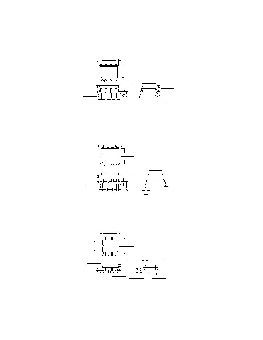
8-Lead Plastic DIP
(N-8)
OUTLINE DIMENSIONS
Dimensions shown in inches and (mm).
8-Lead Narrow Body (SOIC)
(SO-8)
8
1
4
5
0.430 (10.92)
0.348 (8.84)
0.280 (7.11)
0.240 (6.10)
PIN 1
SEATING
PLANE
0.022 (0.558)
0.014 (0.356)
0.060 (1.52)
0.015 (0.38)
0.210 (5.33)
MAX
0.130
(3.30)
MIN
0.070 (1.77)
0.045 (1.15)
0.100
(2.54)
BSC
0.160 (4.06)
0.115 (2.93)
0.325 (8.25)
0.300 (7.62)
0.015 (0.381)
0.008 (0.204)
0.195 (4.95)
0.115 (2.93)
8-Lead Cerdip
(Q-8)
8
1
4
5
0.310 (7.87)
0.220 (5.59)
PIN 1
0.005 (0.13)
MIN
0.055 (1.4)
MAX
SEATING
PLANE
0.023 (0.58)
0.014 (0.36)
0.200 (5.08)
MAX
0.150
(3.81)
MIN
0.070 (1.78)
0.030 (0.76)
0.200 (5.08)
0.125 (3.18)
0.100
(2.54)
BSC
0.060 (1.52)
0.015 (0.38)
0.405 (10.29)
MAX
15
∞
0
∞
0.320 (8.13)
0.290 (7.37)
0.015 (0.38)
0.008 (0.20)
0.1968 (5.00)
0.1890 (4.80)
8
5
4
1
0.2440 (6.20)
0.2284 (5.80)
PIN 1
0.1574 (4.00)
0.1497 (3.80)
0.0688 (1.75)
0.0532 (1.35)
SEATING
PLANE
0.0098 (0.25)
0.0040 (0.10)
0.0192 (0.49)
0.0138 (0.35)
0.0500
(1.27)
BSC
0.0098 (0.25)
0.0075 (0.19)
0.0500 (1.27)
0.0160 (0.41)
8
∞
0
∞
0.0196 (0.50)
0.0099 (0.25)
x 45
∞

≠15≠

8/21/97 4:00 PM
OP297
≠16≠
REV. D
000000000
PRINTED IN U.S.A.