 | –≠–ª–µ–∫—Ç—Ä–æ–Ω–Ω—ã–π –∫–æ–º–ø–æ–Ω–µ–Ω—Ç: OP400GS | –°–∫–∞—á–∞—Ç—å:  PDF PDF  ZIP ZIP |

REV. 0
Information furnished by Analog Devices is believed to be accurate and
reliable. However, no responsibility is assumed by Analog Devices for its
use, nor for any infringements of patents or other rights of third parties
which may result from its use. No license is granted by implication or
otherwise under any patent or patent rights of Analog Devices.
a
120 kHz Bandwidth, Low Distortion,
Isolation Amplifier
AD215
© Analog Devices, Inc., 1996
One Technology Way, P.O. Box 9106, Norwood, MA 02062-9106, U.S.A.
Tel: 617/329-4700
Fax: 617/326-8703
FUNCTIONAL BLOCK DIAGRAM
FEATURES
Isolation Voltage Rating: 1,500 V rms
Wide Bandwidth: 120 kHz, Full Power (≠3 dB)
Rapid Slew Rate: 6 V/ s
Fast Settling Time: 9 s
Low Harmonic Distortion: ≠80 dB @ 1 kHz
Low Nonlinearity:
0.005%
Wide Output Range:
10 V, min (Buffered)
Built-in Isolated Power Supply:
15 V dc @ 10 mA
Performance Rated over ≠40 C to +85 C
APPLICATIONS INCLUDE
High Speed Data Acquisition Systems
Power Line and Transient Monitors
Multichannel Muxed Input Isolation
Waveform Recording Instrumentation
Power Supply Controls
Vibration Analysis
Flexible Input and Buffered Output Stages: An uncommit-
ted op amp is provided on the input stage of the AD215 to
allow for input buffering or amplification and signal condition-
ing. The AD215 also features a buffered output stage to drive
low impedance loads and an output voltage trim for zeroing the
output offset where needed.
High Accuracy: The AD215 has a typical nonlinearity of
±
0.005% (B grade) of full-scale range and the total harmonic
distortion is typically ≠80 dB at 1 kHz. The AD215 provides
designers with complete isolation of the desired signal without
loss of signal integrity or quality.
Excellent Common-Mode Performance: The AD215BY
(AD215AY) provides 1,500 V rms (750 V rms) common-mode
voltage protection from its input to output. Both grades feature
a low common-mode capacitance of 4.5 pF inclusive of the
dc/dc power isolation. This results in a typical common-mode
rejection specification of 105 dB and a low leakage current of
2.0
µ
A rms max (240 V rms, 60 Hz).
Isolated Power: An unregulated isolated power supply of
±
15 V dc @
±
10 mA is available at the isolated input port of
the AD215. This permits the use of ancillary isolated front-end
amplifiers or signal conditioning components without the need
for a separate dc/dc supply. Even the excitation of transducers
can be accomplished in most applications.
Rated Performance over the ≠40 C to +85 C Temperature
Range: With an extended industrial temperature range rating,
the AD215 is an ideal isolation solution for use in many indus-
trial environments.
GENERAL DESCRIPTION
The AD215 is a high speed input isolation amplifier designed to
isolate and amplify wide bandwidth analog signals. The innova-
tive circuit and transformer design of the AD215 ensures wide-
band dynamic characteristics while preserving key dc performance
specifications.
The AD215 provides complete galvanic isolation between the
input and output of the device including the user-available
front-end isolated power supplies. The functionally complete
design, powered by a
±
15 V dc supply, eliminates the need for a
user supplied isolated dc/dc converter. This permits the designer
to minimize circuit overhead and reduce overall system design
complexity and component costs.
The design of the AD215 emphasizes maximum flexibility and
ease of use in a broad range of applications where fast analog
signals must be measured under high common-mode voltage
(CMV) conditions. The AD215 has a
±
10 V input/output
range, a specified gain range of 1 V/V to 10 V/V, a buffered out-
put with offset trim and a user-available isolated front-end
power supply which produces
±
15 V dc at
±
10 mA.
PRODUCT HIGHLIGHTS
High Speed Dynamic Characteristics: The AD215 features
a typical full-power bandwidth of 120 kHz (100 kHz min), rise
time of 3
µ
s and settling time of 9
µ
s. The high speed perfor-
mance of the AD215 allows for unsurpassed galvanic isolation
of virtually any wideband dynamic signal.
OUT HI
TRIM
OUT LO
+15V
IN
≠15V
IN
PWR RTN
FB
IN≠
IN+
IN COM
+V
ISO
≠V
ISO
1
3
MODULATOR
37
36
38
42
44
43
6
2
5
4
UNCOMMITTED
INPUT OP AMP
R
R
OUTPUT
BUFFER
33k
0.01µF
DEMODULATOR
LOW-PASS
FILTER
150kHz
POWER
ISOLATED
DC
SUPPLY
430kHz
POWER
OSCILLATOR
T1
T2
AD215
SIGNAL

REV. 0
≠2≠
AD215≠SPECIFICATIONS
(Typical @ +25 C, V
S
= 15 V dc, 2 k
output load, unless otherwise noted.)
AD215AY/BY
Parameter
Conditions
Min
Typ
Max
Units
GAIN
Range
1
1
10
V/V
Error
G = 1 V/V, No Load on V
ISO
±
0.5
±
2
%
vs. Temperature
0
∞
C to +85
∞
C
+15
ppm/
∞
C
≠40
∞
C to 0
∞
C
+50
ppm/
∞
C
vs. Supply Voltage
±
(14.5 V dc to 16.5 V dc)
+100
ppm/V
vs. Isolated Supply Load
2
+20
ppm/mA
Nonlinearity
3
AD215BY Grade
±
10 V Output Swing, G = 1 V/V
±
0.005
±
0.015
%
±
10 V Output Swing, G = 10 V/V
±
0.01
%
AD215AY Grade
±
10 V Output Swing, G = 1 V/V
±
0.01
±
0.025
%
±
10 V Output Swing, G = 10 V/V
±
0.025
%
INPUT VOLTAGE RATINGS
Input Voltage Rating
G = 1 V/V
±
10
V
Maximum Safe Differential Range
IN+ or IN≠, to IN COM
±
15
V
CMRR of Input Op Amp
100
dB
Isolation Voltage Rating
4
Input to Output, AC, 60 Hz
AD215BY Grade
100% Tested
4
1500
V rms
AD215AY Grade
100% Tested
4
750
V rms
IMRR (Isolation Mode Rejection Ratio)
R
S
100
(IN+ & IN≠), G = 1 V/V, 60 Hz
120
dB
R
S
100
(IN+ & IN≠), G = 1 V/V, 1 kHz
100
dB
R
S
100
(IN+ & IN≠), G = 1 V/V, 10 kHz
80
dB
R
S
1 k
(IN+ & IN≠), G = 1 V/V, 60 Hz
105
dB
R
S
1 k
(IN+ & IN≠), G = 1 V/V, 1 kHz
85
dB
R
S
1 k
(IN+ & IN≠), G = 1 V/V, 10 kHz
65
dB
Leakage Current, Input to Output
240 V rms, 60 Hz
2
µ
A rms
INPUT IMPEDANCE
Differential
G = 1 V/V
16
M
Common Mode
2 4.5
G
pF
INPUT OFFSET VOLTAGE
Initial
@ +25
∞
C
±
0.4
±
2.0
mV
vs. Temperature
0
∞
C to +85
∞
C
±
2
µ
V/
∞
C
≠40
∞
C to 0
∞
C
±
20
µ
V/
∞
C
OUTPUT OFFSET VOLTAGE
Initial
@ +25
∞
C, Trimmable to Zero
0
≠35
≠80
mV
vs. Temperature
0
∞
C to +85
∞
C
±
30
µ
V/
∞
C
≠40
∞
C to 0
∞
C
±
80
µ
V/
∞
C
vs. Supply Voltage
±
350
µ
V/V
vs. Isolated Supply Load
2
≠35
µ
V/mA
INPUT BIAS CURRENT
Initial
@ +25
∞
C
300
nA
vs. Temperature
≠40
∞
C to +85
∞
C
±
400
nA
INPUT DIFFERENCE CURRENT
Initial
@ +25
∞
C
±
3
nA
vs. Temperature
≠40
∞
C to +85
∞
C
±
40
nA
INPUT VOLTAGE NOISE
Input Voltage Noise
Frequency > 10 Hz
20
nV/
Hz
DYNAMIC RESPONSE (2 k
Load)
Full Signal Bandwidth (≠3 dB)
G = 1 V/V, 20 V pk-pk Signal
100
120
kHz
Transport Delay
6
2.2
µ
s
Slew Rate
±
10 V Output Swing
6
V/
µ
s
Rise Time
10% to 90%,
±
10 V Output Swing
3
µ
s

AD215
REV. 0
≠3≠
AD215AY/BY
Parameter
Conditions
Min
Typ
Max
Units
DYNAMIC RESPONSE (2 k
Load) Cont.
Settling Time
to
±
0.10%,
±
10 V Output Swing
9
µ
s
Overshoot
1
%
Harmonic Distortion Components
@ 1 kHz
≠80
dB
@ 10 kHz
≠65
dB
Overload Recovery Time
G = 1 V/V,
±
15 V Drive
5
µ
s
Output Overload Recovery Time
G > 5
10
µ
s
RATED OUTPUT
Voltage
Out HI to Out LO
±
10
V
Current
2 k
Load
±
5
mA
Max Capacitive Load
500
pF
Output Resistance
1
Output Ripple and Noise
7
1 MHz Bandwidth
10
mV pk-pk
50 kHz Bandwidth
2.5
mV pk-pk
ISOLATED POWER OUTPUT
8
Voltage
No Load
±
14.25
±
15
±
17.25
V
vs. Temperature
0
∞
C to +85
∞
C
+20
mV/
∞
C
≠40
∞
C to 0
∞
C
+25
mV/
∞
C
Current at Rated Supply Voltage
2, 9
±
10
mA
Regulation
No Load to Full Load
≠90
mV/V
Line Regulation
290
mV/V
Ripple
1 MHz Bandwidth, No Load
2
50
mV rms
POWER SUPPLY
Supply Voltage
Rated Performance
±
14.5
±
15
±
16.5
V dc
Operating
10
±
14.25
±
17
V dc
Current
Operating (+15 V dc/≠15 V dc Supplies)
+40/≠18
mA
TEMPERATURE RANGE
Rated Performance
≠40
+85
∞
C
Storage
≠40
+85
∞
C
NOTES
1
1
The gain range of the AD215 is specified from 1 to 10 V/V. The AD215 can also be used with gains of up to 100 V/V. With a gain of 100 V/V a 20% reduction in the
≠3 dB bandwidth specification occurs and the nonlinearity degrades to
±
0.02% typical.
1
2
When the isolated supply load exceeds
±
1 mA, external filter capacitors are required in order to ensure that the gain, offset, and nonlinearity specifications are pre-
served and to maintain the isolated supply full load ripple below the specified 50 mV rms. A value of 6.8
µ
F is recommended.
1
3
Nonlinearity is specified as a percent (of full-scale range) deviation from a best straight line.
1
4
The isolation barrier (and rating) of every AD215 is 100% tested in production using a 5 second partial discharge test with a failure detection threshold of 150 pC. All
"B" grade devices are tested with a minimum voltage of 1,800 V rms. All "A" grade devices are tested with a minimum voltage of 850 V rms.
1
5
The AD215 should be allowed to warm up for approximately 10 minutes before any gain and/or offset adjustments are made.
1
6
Equivalent to a 0.8 degrees phase shift.
1
7
With the
±
15 V dc power supply pins bypassed by 2.2
µ
F capacitors at the AD215 pins.
1
8
Caution: The AD215 design does not provide short circuit protection of its isolated power supply. A current limiting resistor may be placed in series with the isolated
power terminals and the load in order to protect the supply against inadvertent shorts.
1
9
With an input power supply voltage greater than or equal
±
15 V dc, the AD215 may supply up to
±
15 mA from the isolated power supplies.
10
Voltages less than 14.25 V dc may cause the AD215 to cease operating properly. Voltages greater than
±
17.5 V dc may damage the internal components of the
AD215 and consequently should not be used.
Specifications subject to change without notice.
WARNING!
ESD SENSITIVE DEVICE
CAUTION
ESD (electrostatic discharge) sensitive device. Electrostatic charges as high as 4000 V readily
accumulate on the human body and test equipment and can discharge without detection.
Although the AD215 features proprietary ESD protection circuitry, permanent damage may
occur on devices subjected to high energy electrostatic discharges. Therefore, proper ESD
precautions are recommended to avoid performance degradation or loss of functionality.
AD215
REV. 0
≠4≠
OUT HI
TRIM
OUT LO
+15V
IN
≠15V
IN
PWR RTN
AD215
SIGNAL
1
3
UNCOMMITTED
INPUT OP AMP
FB
IN≠
IN+
POWER
T2
T1
33k
R
R
0.01µF
OUTPUT
BUFFER
IN COM
+V
ISO
≠V
ISO
MODULATOR
DEMODULATOR
LOW-PASS
FILTER
150kHz
37
36
38
42
44
43
430kHz
POWER
OSCILLATOR
6
2
5
ISOLATED
DC
SUPPLY
4
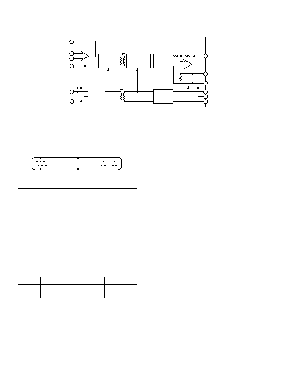
Figure 1. Functional Block Diagram
PIN CONFIGURATIONS
36 38
37
42 44
43
BOTTOM VIEW OF
FOOTPRINT
4
6
2
3
5
1
AD215 PIN DESIGNATIONS
Pin
Designation
Function
1
IN+
Noninverting Input
2
IN COM
Input Common
3
IN≠
Inverting Input
4
FB
Amplifier Feedback
5
≠V
ISO
OUT
Isolated ≠15 V dc Power Supply
6
+V
ISO
OUT
Isolated +15 V dc Power Supply
36
TRIM
Output Offset Trim Adjust
37
OUT LO
Output Low
38
OUT HI
Output High
42
+15 V
IN
+15 V dc Power
43
PWR RTN
±
15 V dc Power Supply Common
44
≠15 V
IN
≠15 V dc Power
ORDERING GUIDE
Model
Temperature Range
V
CMV
Nonlinearity
*
AD215AY
≠40
∞
C to +85
∞
C
750
0.01%
AD215BY
≠40
∞
C to +85
∞
C
1500
0.005%
*Typical @ +25
∞
C, G = 1 V/V.
INSIDE THE AD215
The AD215 is a fully self-contained analog signal and power
isolation solution. It employs a double-balanced amplitude
modulation technique to perform transformer coupling of sig-
nals ranging in frequency from true dc values to those having
frequencies of 120 kHz or less.
To generate the power supplies used for the isolated front-end
circuitry, an internal clock oscillator drives the primary winding
of the integral dc/dc power supply's transformer, T2. The
resultant voltage developed across the secondary winding is
then rectified and filtered for use as the isolated power supply.
This built-in isolated dc/dc converter provides sufficient power
for both the internal isolated circuit elements of the AD215 as
well as any ancillary components supplied by the user. It saves
onboard space and component cost where additional amplifica-
tion or signal conditioning is required.
After an input signal is amplified by the uncommitted op amp,
it is modulated at a carrier frequency of approximately 430 kHz
and applied across the primary winding of the signal isolation
transformer T1.
The resultant signal induced on the secondary winding of the
transformer is then demodulated and filtered using a low-pass
Bessel response filter set at a frequency of 150 kHz. The func-
tion of the filter reconstructs the original signal as it appears on
the input.
The signal transformer design and construction allow non-
linearity to be independent of both the specified temperature
and gain ranges.
After complete reconstruction, the signal is subjected to an off-
set trim stage and final output buffer. The trim circuit allows
the designer flexibility to adjust for any offset as desired.

Performance Characteristics≠AD215
REV. 0
≠5≠
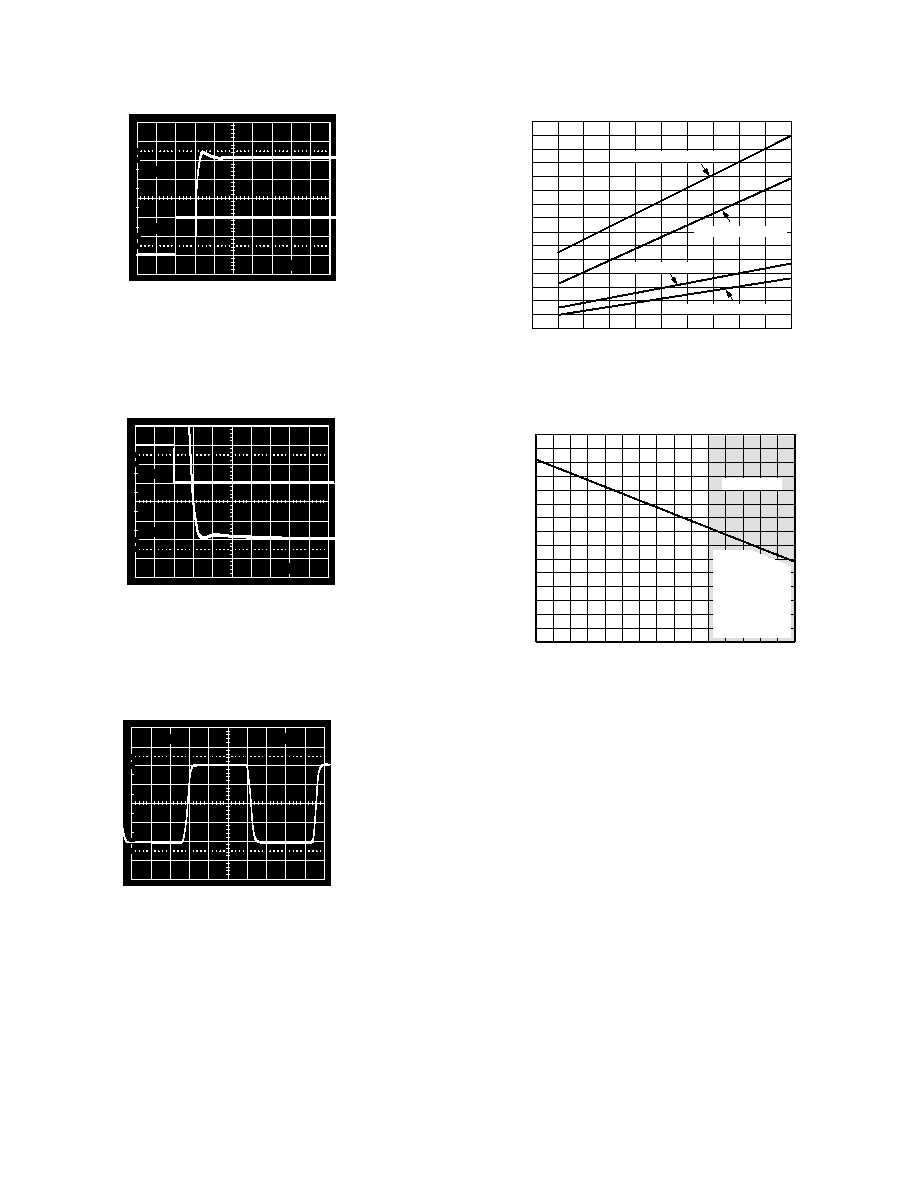
TEMPERATURE ≠
∞
C
GAIN ERROR ≠ %
0.10
≠0.25
≠40
100
≠20
0
20
40
60
80
0.05
≠0.05
≠0.10
≠0.15
≠0.20
0
Figure 2. Gain Error vs. Temperature
10
0%
100
90
1mV
+1
0
≠1
+0.004
≠0.004
≠10 ≠8
≠6
≠4
≠2
0
2
4
6
8
10
NONLINEARITY ≠ mV
NONLINEARITY ≠ %
OUTPUT VOLTAGE ≠ Volts
Figure 3. Gain Nonlinearity vs. Output Voltage (G = 1 V/V)
FREQUENCY ≠ Hz
150
140
60
10
100k
100
CMR ≠ dB
1k
10k
130
120
110
100
90
80
70
R
S
100
R
S
1k
Figure 4. Typical Common-Mode Rejection vs. Frequency
INPUT SIGNAL FREQUENCY ≠ kHz
1
0
≠12
0.1
1000
1.0
GAIN ≠ dB
10
100
≠1
≠2
≠3
≠4
≠5
≠6
≠7
≠8
≠9
≠10
≠11
G = 100
G = 10
G = 1
Figure 5. Normalized Gain as a Function of Signal
Frequency
3
2
1
0
0
45
90
130
10
20
30
40
50
60
70
80
90 100 110 120
FREQUENCY ≠ kHz
G = 100
G =10
G = 1
G = 100
G =10
G = 1
PHASE SHIFT ≠ Degrees
TRANSPORT
DELAY ≠ µs
Figure 6. Phase Shift and Transport Delay vs. Frequency
AD215≠Performance Characteristics
REV. 0
≠6≠
10
0%
100
90
5V
100mV
OUTPUT
INPUT
(+10V STEP)
OVERSHOOT
5µs
Figure 7a. Overshoot to a Full-Scale Step Input
(G = 1 V/V)
10
0%
100
90
5µs
5V
100mV
INPUT
(≠10V STEP)
OUTPUT
UNDERSHOOT
Figure 7b. Undershoot to a Full-Scale Input
(G = 1 V/V)
10
0%
100
90
10µs
5V
±
10V, 15kHz STEP OUTPUT RESPONSE (G=1)
Figure 8. Output Response to Full-Scale Step Input
(G = 1 V/V)
V
ISO
LOAD ≠ mA
60
36
0
0
10
1
2
3
4
5
6
7
8
9
56
40
32
24
48
44
28
52
16
20
12
4
8
0.33µF BYPASS CAPS
1.0µF BYPASS CAPS
3.3µF BYPASS CAPS
10µF BYPASS CAPS
V
ISO
RIPPLE ≠ mV p-p
Figure 9.
±
V
ISO
Supply Ripple vs. Load
V
ISO
LOAD ≠
±
mA
16.2
15.2
14.8
15
5
10
16.0
15.4
15.8
15.6
15.0
V
ISO
≠
±
V
V
S
=
±
15V dc
NOTE:
THE GAIN AND
OFFSET ERRORS
WILL INCREASE
WHEN THE
ISOLATED
POWER SUPPLY
LOAD EXCEEDS
±
10mA
Figure 10.
±
V
ISO
Supply Voltage vs. Load
AD215
REV. 0
≠7≠
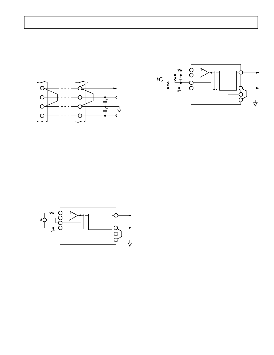
POWERING THE AD215
The AD215 is powered by a bipolar
±
15 V dc power supply
connected as shown in Figure 11. External bypass capacitors
should be provided in bused applications. Note that a small
signal-related current (50 mA/V
OUT
) will flow out of the OUT
LO pin (Pin 37). Therefore, the OUT LO terminals should be
bused together and referenced at a single "Analog Star Ground"
to the
±
15 V dc supply common as illustrated Figure 11.
AD215
N
AD215
1
OUT LO
N
N
TH
CHANNEL
1
ST
CHANNEL
ANALOG STAR GROUND
OUT LO
1
SIG COM
+V
IN
PWR RTN
≠V
IN
+15V dc
COM
≠15V dc
2.2µF
37
42
43
44
42
44
43
2.2µF
37
Figure 11. Typical Power Supply Connections
Power Supply Voltage Considerations
The rated performance of the AD215 remains unaffected for
power supply voltages in the
±
14.5 V dc to
±
16.5 V dc range.
Voltages below
±
14.25 V dc may cause the AD215 to cease op-
erating properly.
Note: Power supply voltages greater than
±
17.5 V dc may damage
the internal components and consequently should not be used.
USING THE AD215
Unity Gain Input Configuration
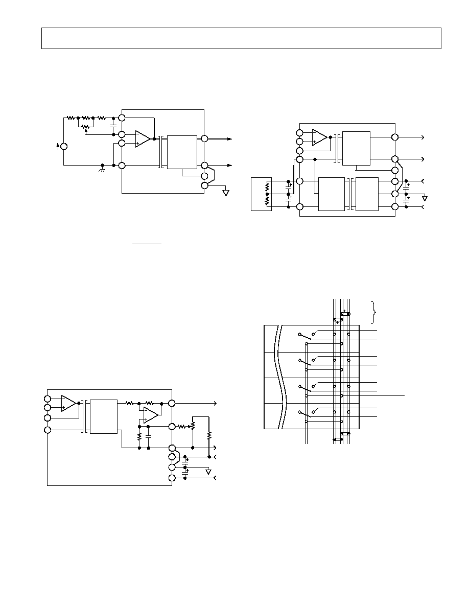
The basic unity gain configuration for input signals of up to
±
10 V is shown in Figure 12.
R
IN
= 2k
V
SIGNAL
IN+
IN≠
FB
IN COM
OUT HI
OUT LO
PWR
RTN
COM
TRIM
OUTPUT FILTER,
BUFFER AND
TRIM CIRCUITRY
1
3
4
2
38
36
37
43
AD215
Figure 12. Basic Unity Gain
Noninverting Configuration for Gain Greater Than Unity
Figure 13 shows how to achieve a gain greater than one while
continuing to preserve a very high input impedance. A recom-
mended PC board layout for multichannel applications is shown
in Figure 20b.
R
IN
= 2k
V
SIGNAL
IN+
IN≠
FB
IN COM
OUT HI
OUT LO
PWR
RTN
COM
TRIM
OUTPUT
FILTER,
BUFFER
AND
TRIM
CIRCUITRY
1
3
4
2
38
36
37
43
AD215
C
F
47pF
R
F
R
G
Figure 13. Noninverting Input Configuration for
Gain > 1 V/V
In this circuit, the gain equation is as follows:
V
O
= (1 + R
F
/R
G
)
◊
V
SIG
where:
V
O
= Output Voltage (V)
V
SIG
= Input Signal Voltage (V)
R
F
= Feedback Resistor Value (
)
R
G
= Gain Resistor Value (
)
The values for resistors R
F
and R
G
are subject to the following
constraints:
∑ The total impedance of the gain network should be less than
10 k
.
∑ The current drawn in R
F
is less than 1 mA at
±
10 V. Note that
for each mA drawn by the feedback resistor, the isolated
power supply drive capability decreases by 1 mA.
∑ Amplifier gain is set by the feedback (R
F
) and gain resistor
(R
G
).
It is recommended that R
F
is bypassed with a 47 pF capacitor as
shown.
Note: The 2 k
input resistor (R
IN
) in series with the input
signal source and the IN+ terminal in Figures 12 and 13 is rec-
ommended to limit the current at the input terminals of the to
5.0 mA when the AD215 is not powered.
AD215
REV. 0
≠8≠
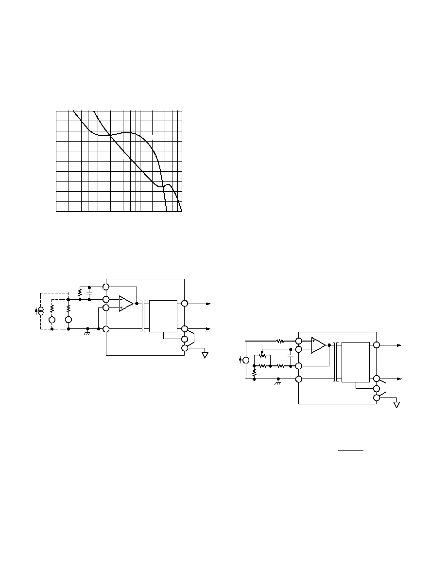
Compensating the Uncommitted Input Op Amp
The open-loop gain and phase versus frequency for the uncom-
mitted input op amp are given in Figure 14. These curves can
be used to determine appropriate values for the feedback resis-
tor (R
F
) and compensation capacitor (C
F
) to ensure frequency
stability when reactive or nonlinear components are used.
FREQUENCY ≠ Hz
100k
100M
1M
AVERAGE VOLTAGE GAIN ≠ dB
10M
25
20
≠25
15
10
5
0
≠5
≠10
≠15
≠20
PHASE
GAIN
ÿ, EXCESS PHASE ≠ Degrees
80
100
280
120
140
160
180
200
220
240
260
Figure 14. Open-Loop Gain and Frequency Response
Inverting, Summing or Current Input Configuration
Figure 14 shows how the AD215 can measure currents or sum
currents or voltages.
V
S1
IN+
IN≠
FB
IN COM
OUT HI
OUT LO
PWR
RTN
COM
TRIM
OUTPUT
FILTER,
BUFFER
AND
TRIM
CIRCUITRY
1
3
4
2
38
36
37
43
AD215
C
F
47pF
R
F
R
S1
V
S2
R
S2
I
S
Figure 15. Noninverting Summing/Current Configuration
For this circuit, the output voltage equation is:
V
O
= ≠R
F
◊
(I
S
+ V
S1
/R
S1
+ V
S2
/R
S2
+ . . .)
where:
V
= Output Voltage (V)
V
S1
= Input Voltage Signal 1 (V)
V
S2
= Input Voltage Signal 2 (V)
I
S
= Input Current Source (A)
R
F
= Feedback Resistor (
) (10 k
, typ)
R
S1
= Input Signal 1 Source Resistance (
)
R
S2
= Input Signal 2 Source Resistance (
)
The circuit of Figure 15 can also be used when the input signal
is larger than the
±
10 V input range of the isolator. For example,
in Figure 15, if only V
S1
, R
S1
and R
F
were connected as shown
with the solid lines, the input voltage span of V
S1
could accom-
modate up to
±
50 V when R
F
= 10 k
and R
S1
= 50 k
.
GAIN AND OFFSET ADJUSTMENTS
General Comments
The AD215 features an output stage TRIM pin useful for zero-
ing the output offset voltage through use of user supplied circuitry.
When gain and offset adjustments are required, the actual com-
pensation circuit ultimately used depends on the following:
∑ The input configuration mode of the isolation amplifier (non-
inverting or inverting).
∑ The placement of any adjusting potentiometer (on the
isolator's input or output side).
As a general rule:
∑ Gain adjustments should be accomplished at the gain-setting
resistor network at the isolator's input.
∑ To ensure stability in the gain adjustment, potentiometers
should be located as close as possible to the isolator's input
and its impedance should be kept low. Adjustment ranges
should also be kept to a minimum since their resolution and
stability is dependent upon the actual potentiometers used.
∑ Output adjustments may be necessary where adjusting poten-
tiometers placed near the input would present a hazard to the
user due to the presence of high common-mode voltages dur-
ing the adjustment procedure.
∑ It is recommended that input offset adjustments are made
prior to gain adjustments.
∑ The AD215 should be allowed to warm up for approximately
10 minutes before gain or offset adjustments are made.
Input Gain Adjustments for Noninverting Mode
Figure 16 shows a suggested noninverting gain adjustment cir-
cuit. Note that the gain adjustment potentiometer R
P
is incorpo-
rated into the gain-setting resistor network.
R
IN
= 2k
V
SIGNAL
IN+
IN≠
FB
IN COM
OUT HI
OUT LO
PWR
RTN
COM
TRIM
OUTPUT
FILTER,
BUFFER
AND
TRIM
CIRCUITRY
1
3
4
2
38
36
37
43
AD215
C
F
0.47pF
R
F
R
G
R
C
R
P
Figure 16. Gain Adjustment for Noninverting Configuration
For a
±
1% trim range:
(R
P
1k
), R
C
0.02
◊
R
G
◊
R
F
R
G
+
R
F
AD215
REV. 0
≠9≠
Input Gain Adjustments for the Inverting Mode
Figure 17 shows a suggested inverting gain adjustment circuit.
In this circuit, gain adjustment is made using a potentiometer
(R
P
) in the feedback loop. The adjustments are effective for all
gains in the 1 to 10 V/V range.
V
SIGNAL
R
F
R
C
R
IN
IN+
IN≠
FB
IN COM
OUT HI
OUT LO
PWR
RTN
COM
TRIM
OUTPUT
FILTER,
BUFFER
AND
TRIM
CIRCUITRY
1
3
4
2
38
36
37
43
AD215
C
F
47pF
R
F
1k
Figure 17. Gain Adjustment for Inverting Configuration
For an approximate
±
1% gain trim range,
R
X
=
R
IN
◊
R
F
R
IN
+
R
F
and select
R
C
= 0.02
◊
R
IN
while
R
F
< 10 k
C
F
= 47 pF
Note: R
F
and R
IN
should have matched temperature coefficient
drift characteristics.
Output Offset Adjustments
Figure 18 illustrates one method of adjusting the output offset
voltage. Since the AD215 exhibits a nominal output offset of
≠35 mV, the circuit shown was chosen to yield an offset correc-
tion of 0 mV to +73 mV. This results in a total output offset
range of approximately ≠35 mV to +38 mV.
IN+
IN≠
FB
IN COM
OUT HI
OUT LO
COM
TRIM
LOW-PASS
FILTER,
(150k
)
1
3
4
2
38
AD215
R
T
1M
R
S
100k
R
P2
10k
OUTPUT
BUFFER
33k
0.01µF
37
36
42
+15V
IN
PWR RTN
≠15V
IN 44
43
2.2µF
2.2µF
≠15V dc
+15V dc
Figure 18. Output Offset Adjustment Circuit
Output Gain Adjustments
Since the output amplifier stage of the AD215 is fixed at unity
gain, any adjustments can be made only in a subsequent stage.
USING ISOLATED POWER
Each AD215 provides an unregulated, isolated bipolar power
source of
±
15 V dc @
±
10 mA, referred to the input common.
This source may be used to power various ancillary components
such as signal conditioning and/or adjustment circuitry, refer-
ences, op amps or remote transducers. Figure 19 shows typical
connections.
IN+
IN≠
FB
IN COM
OUT HI
OUT LO
COM
TRIM
1
3
4
2
AD215
37
36
+V
S
PWR
RTN
≠V
S
43
2.2µF
2.2µF
≠15V dc
+15V dc
+V
ISO
≠V
ISO
C1
6.8µF
6
C2
6.8µF
5
1.5k
1.5k
LOAD
ISOLATED
DC
SUPPLY
430kHz
POWER
OSCIL-
LATOR
OUTPUT
FILTER,
BUFFER
AND
TRIM
CIRCUITRY
42
44
38
Figure 19. Using the Isolated Power Supplies
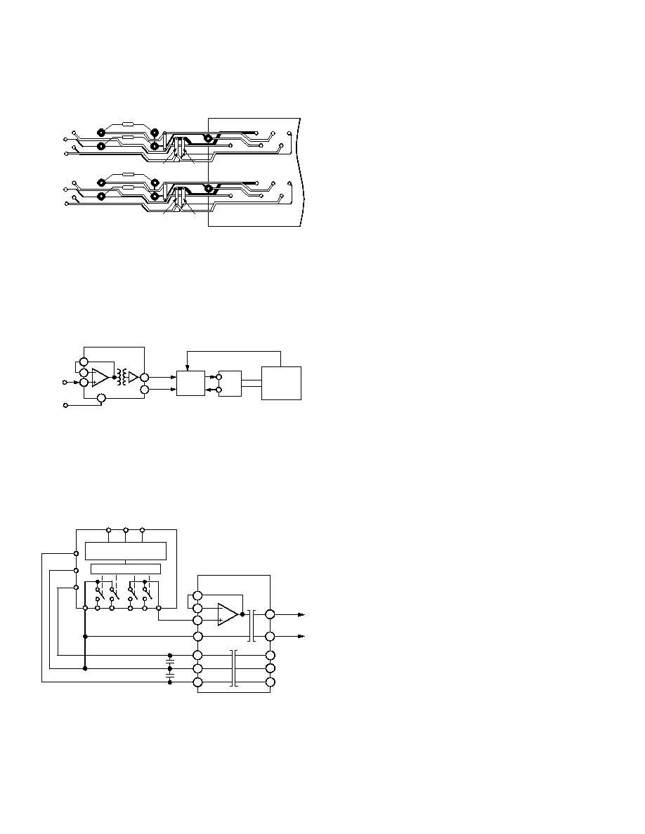
PCB LAYOUT FOR MULTICHANNEL APPLICATIONS
The pin out of the AD215 has been designed to easily facilitate
multichannel applications. Figure 20a shows a recommended
circuit board layout for a unity gain configuration.
38
36
42
44
37
43
38
36
42
44
37
43
38
36
42
44
37
43
38
36
42
44
37
43
2.2µF
2.2µF
2.2µF
2.2µF
+15V dc
≠15V dc
PWR
RTN
SUPPLY BYPASS
CAPACITORS FOR
EVERY FOUR
AD215s
OUT HI
0
TRIM
0
OUT HI
1
TRIM
1
OUT HI
2
TRIM
2
OUT HI
3
TRIM
3
ANALOG
STAR
GROUND
Figure 20a. PCB Layout for Unity Gain
CAUTION
The AD215 design does not provide short-circuit protection of
its isolated power supply. A current limiting resistor should be
placed in series with the supply terminals and the load in order
to protect against inadvertent shorts.
AD215
REV. 0
≠10≠
When gain setting resistors are used, 0.325" channel centers can
still be achieved as shown in Figure 20b.
R
G
R
F
C
F
C2
C1
1
2
3
4
5
6
IN
IN COM
+V
ISO
≠VI
SO
C1, C2 ARE V
ISO
FILTER CAPACITORS.
R
F
, R
G
ARE FEEDBACK, GAIN RESISTORS.
C
F
IS A FEEDBACK BYPASS CAPACITOR.
R
G
R
F
C
F
C2
C1
1
2
3
4
5
6
IN
IN COM
+V
ISO
≠VI
SO
Figure 20b. PCB Layout for Gain Greater than Unity
APPLICATIONS EXAMPLES
Motor Control
Figure 21 shows an AD215 used in a dc motor control applica-
tion. Its excellent phase characteristics and wide bandwidth are
ideal for this type of application.
1
3
4
38
37
AD215
MOTOR
COMMAND
±
10 VOLTS
2
COM
G = 1
ISOLATED
MOTOR
COMMAND
±
10V V
C
OUT LO
SHAFT
I
MOTOR
MOTOR
OPTICAL
RESOLVER
OR
TACHOMETER
ENCODER
ENCODER FEEDBACK
MOTOR
CONTROL
UNIT
Figure 21. Motor Control Application
Multichannel Data Acquisition
The current drive capabilities of the AD215's bipolar
±
15 V dc
isolated power supply is more than adequate to meet the modest
±
800
µ
A supply current requirements for the AD7502 multi-
plexer. Digital isolation techniques should be employed to iso-
late the Enable (EN), A0 and A1 logic control signals.
IN+
IN≠
FB
IN COM
OUT HI
OUT LO
1
3
4
AD215
PWR
RTN
≠15V
+15V
+V
ISO
≠V
ISO
6.8µF
6
6.8µF
G = 1
42
38
(≠15V)
GND
(+15V)
EN
A1
A0
AD7502
37
2
5
2
COM
43
44
S1 ≠ S4
S5 ≠ S8
DTL/TTL TO CMOS LEVEL
TRANSLATOR
DECODER/DRIVER
Figure 22. Multichannel Data Acquisition Application
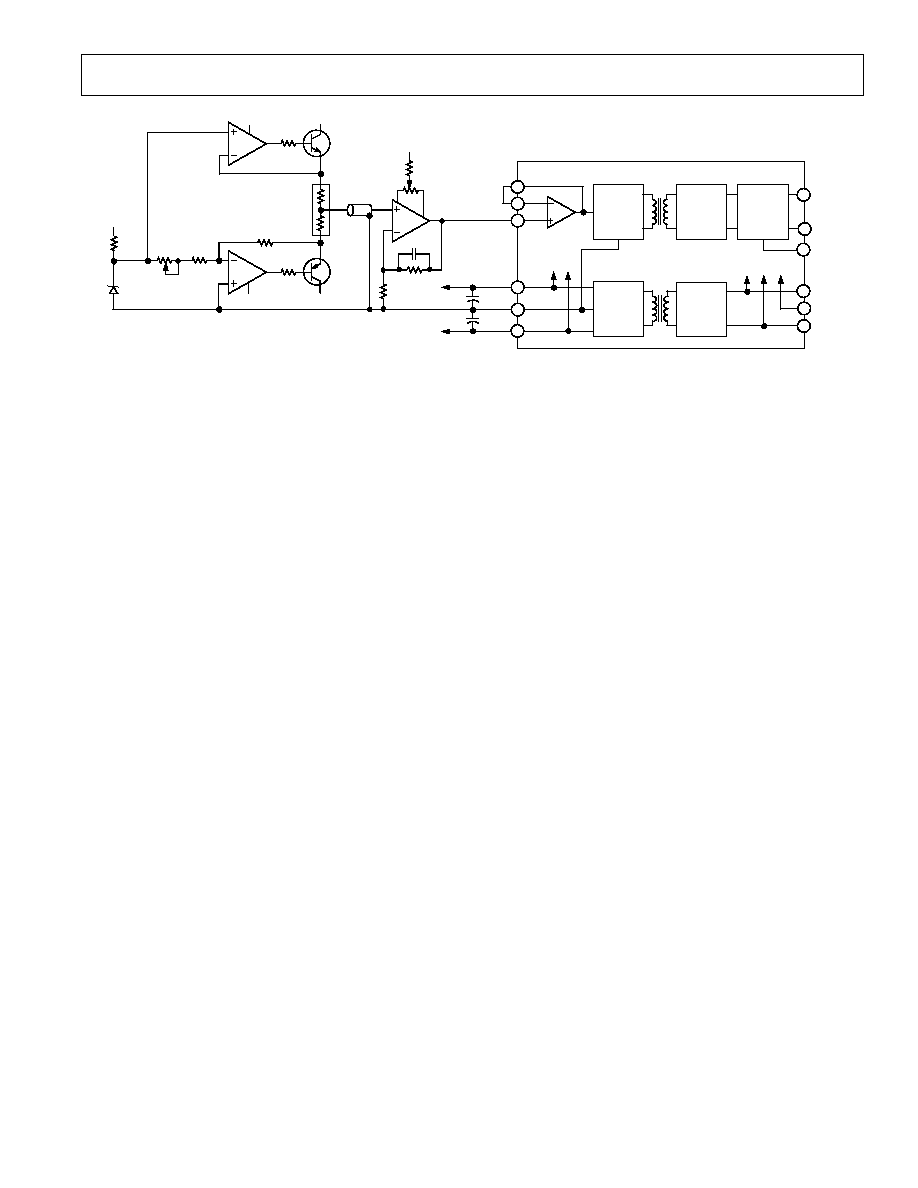
AC Transducer Applications
In applications such as vibration analysis, where the user must
acquire and process the spectral content of a sensor's signal
rather than its "dc" level, the wideband characteristics of the
AD215 prove most useful. Key specifications for ac transducer
applications include bandwidth, slew rate and harmonic distor-
tion. Since the transducer may be mechanically bonded or
welded to the object under test, isolation is typically required to
eliminate ground loops as well as protect the electronics used in
the data acquisition system. Figure 23 shows an isolated strain
gage circuit employing the AD215 and a high speed operational
amplifier (AD744).
To alleviate the need for an instrumentation amplifier, the
bridge is powered by a bipolar excitation source. Under this ap-
proach the common-mode voltage is
±
V
SPAN
which is typically
only a few millivolts, rather than the V
EXC
2 that would be
achieved with a unipolar excitation source and Wheatstone
bridge configuration.
Using two strain gages with a gage factor of 3 mV/V and a
±
1.2 V excitation signal, a
±
6.6 mV output signal will result. A
gain setting of 454 will scale this low level signal to
±
3 V, which
can then be digitized by a high speed, 100 kHz sampling ADC
such as the AD7870.
The low voltage excitation is used to permit the front-end cir-
cuitry to be powered from the isolated power supplies of the
AD215, which can supply up to
±
10 mA of isolated power at
±
15 V. The bridge draws only 3.5 mA, leaving sufficient cur-
rent to power the micropower dual BiFET (400
µ
A quiescent
current) and the high speed AD744 BiFET amplifier (4 mA
quiescent current).
AD215
REV. 0
≠11≠
IN+
IN≠
FB
COM
OUT HI
OUT LO
TRIM
3
4
AD215
36
PWR
RTN
≠15V
+15V
+V
ISO
≠V
ISO
6.8µF
6.8µF
350
≠
350
+
Q1
2N3904
38
+V
ISO
220
+V
ISO
1/2
AD648
220
≠V
ISO
1/2
AD648
9.76k
500
+V
ISO
6.8k
Q2
2N3906
≠V
ISO
AD589
2M
1M
AD744
2.2pF
453k
≠1.2V
+1.2V
10k
≠V
ISO
1k
ISOLATED
DC
SUPPLY
430kHz
POWER
OSC
37
43
42
44
MOD
DEMOD
OUTPUT
FILTER
AND
BUFFER
2
6
5
C2
C1
1
Figure 23. Strain Gage Signal Conditioning Application
AD215
REV. 0
≠12≠
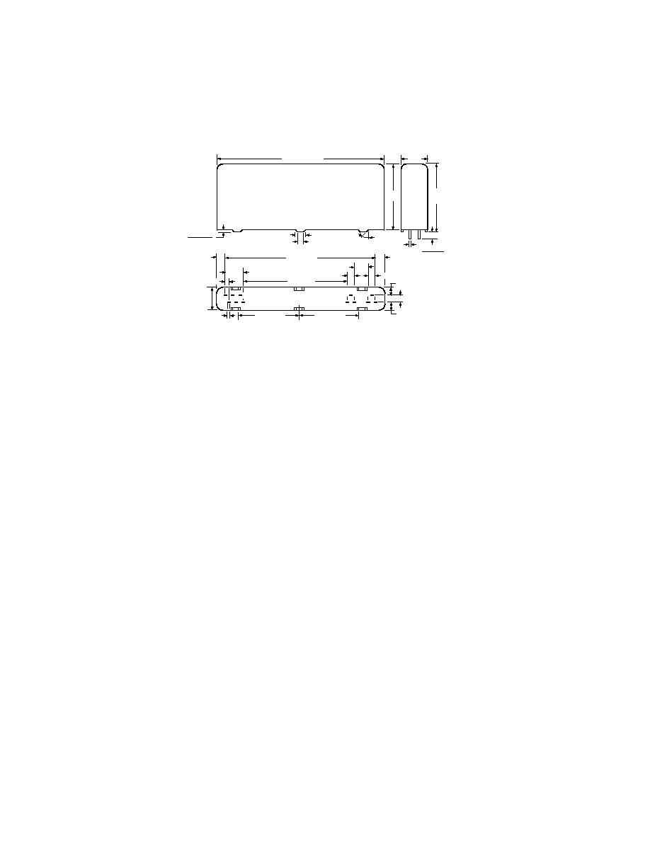
OUTLINE DIMENSIONS
Dimensions shown in inches and (mm).
AD215 SIP PACKAGE
0.094 (2.4)
0.12 (3.0) TYP
30
∞
TYP
0.020 (0.5)
0.015 (0.4)
2.480 (63.0) MAX
0.815
(20.7)
0.010
(0.25)
0.165 (4.2)
0.135 (3.4)
0.840
(21.4)
MAX
0.325 (8.3)
MAX
36 38
37
42 44
43
BOTTOM VIEW OF
FOOTPRINT
0.712 (18.2)
4
6
2
3
5
0.712 (18.2)
0.1
(2.5)
0.11 (2.8)
0.11 (2.8)
0.2
(5.1)
0.1 (2.5)
0.325
(8.3)
MAX
0.022 (0.56)
1.50 (38.1)
1
0.250
(6.4)
2.15 (54.6)
0.05 (1.3)
0.16 (4.1)
0.16 (4.1)
0.1 (2.5)
NOTE: PINS MEASURE 0.022 (0.56) x 0.010 (0.25) PRIOR TO TINNING.
TINNING MAY ADD UP TO 3 mils (0.003") TO THESE DIMENSIONS.
C
L
C2134≠20≠4/96
PRINTED IN U.S.A.