 | –≠–ª–µ–∫—Ç—Ä–æ–Ω–Ω—ã–π –∫–æ–º–ø–æ–Ω–µ–Ω—Ç: OP482 | –°–∫–∞—á–∞—Ç—å:  PDF PDF  ZIP ZIP |
REV. B
Information furnished by Analog Devices is believed to be accurate and
reliable. However, no responsibility is assumed by Analog Devices for its
use, nor for any infringements of patents or other rights of third parties
which may result from its use. No license is granted by implication or
otherwise under any patent or patent rights of Analog Devices.
a
Dual/Quad Low Power, High Speed
JFET Operational Amplifiers
OP282/OP482
One Technology Way, P.O. Box 9106, Norwood, MA 02062-9106, U.S.A.
Tel: 617/329-4700
Fax: 617/326-8703
GENERAL DESCRIPTION
The OP282/OP482 dual and quad operational amplifiers feature
excellent speed at exceptionally low supply currents. Slew rate
exceeds 7 V/
µ
s with supply current under 250
µ
A per amplifier.
These unity gain stable amplifiers have a typical gain bandwidth
of 4 MHz.
The JFET input stage of the OP282/OP482 insures bias current
is typically a few picoamps and below 500 pA over the full
temperature range. Offset voltage is under 3 mV for the dual
and under 4 mV for the quad.
With a wide output swing, within 1.5 volts of each supply, low
power consumption and high slew rate, the OP282/OP482 are
ideal for battery-powered systems or power restricted applica-
tions. An input common-mode range that includes the positive
supply makes the OP282/OP482 an excellent choice for high-
side signal conditioning.
The OP282/OP482 are specified over the extended industrial
temperature range. Both dual and quad amplifiers are available
in plastic and ceramic DIP plus SOIC surface mount packages.
FEATURES
High Slew Rate: 9 V/ s
Wide Bandwidth: 4 MHz
Low Supply Current: 250 A/Amplifier
Low Offset Voltage: 3 mV
Low Bias Current: 100 pA
Fast Settling Time
Common-Mode Range Includes V+
Unity Gain Stable
APPLICATIONS
Active Filters
Fast Amplifiers
Integrators
Supply Current Monitoring
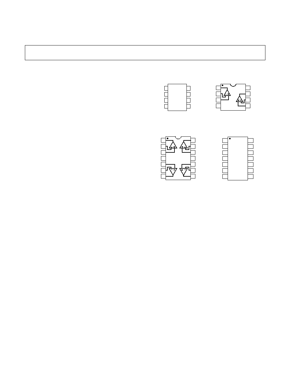
PIN CONNECTIONS
8-Lead Narrow-Body SOIC
8-Lead Epoxy DIP
(S Suffix)
(P Suffix)
1
2
3
4
5
6
7
8
OUT A
≠IN A
+IN A
V≠
OP-482
V+
OUT B
≠IN B
+IN B
OP282
OUT A
≠IN A
+IN A
V≠
V+
OUT B
≠IN B
+IN B
1
2
3
4
5
6
7
8
OP282
14-Lead Epoxy DIP
14-Lead Narrow-Body SOIC
(P Suffix)
(S Suffix)
1
2
3
4
5
6
7
14
13
12
11
10
9
8
OUT A
≠IN A
+IN A
V+
+IN B
≠IN B
OUT B
OUT B
≠IN D
+IN D
V≠
+IN C
≠IN C
OUT C
OP482
1
2
3
4
5
6
7
14
13
12
11
10
9
8
OUT A
≠IN A
+IN A
V+
+IN B
≠IN B
OUT B
OUT D
≠IN D
+IN D
V≠
+IN C
≠IN C
OUT C
OP482

≠2≠
OP282/OP482≠SPECIFICATIONS
ELECTRICAL CHARACTERISTICS
(@ V
S
= 15.0 V, T
A
= +25 C unless otherwise noted)
Parameter
Symbol
Conditions
Min
Typ
Max
Units
INPUT CHARACTERISTICS
Offset Voltage
V
OS
OP282
0.2
3
mV
OP282, ≠40
T
A
+85
∞
C
4.5
mV
Offset Voltage
V
OS
OP482
0.2
4
mV
OP482, ≠40
T
A
+85
∞
C
6
mV
Input Bias Current
I
B
V
CM
= 0 V
3
100
pA
V
CM
= 0 V, Note 1
500
pA
Input Offset Current
I
OS
V
CM
= 0 V
1
50
pA
V
CM
= 0 V, Note 1
250
pA
Input Voltage Range
≠11
+15
V
Common-Mode Rejection
CMR
≠11 V
V
CM
+15 V, ≠40
T
A
+85
∞
C
70
90
dB
Large Signal Voltage Gain
A
VO
R
L
= 10 k
20
V/mV
R
L
= 10 k
, ≠40
T
A
+85
∞
C
15
V/mV
Offset Voltage Drift
V
OS
/
T
10
µ
V/
∞
C
Bias Current Drift
I
B
/
T
8
pA/
∞
C
OUTPUT CHARACTERISTICS
Output Voltage Swing
V
O
R
L
= 10 k
≠13.5
±
13.9 13.5
V
Short Circuit Limit
I
SC
Source
3
10
mA
Sink
≠8
≠12
mA
Open-Loop Output Impedance
Z
OUT
f = 1 MHz
200
POWER SUPPLY
Power Supply Rejection Ratio
PSRR
V
S
=
±
4.5 V to
±
18 V,
≠40
T
A
+85
∞
C
25
316
µ
V/V
Supply Current/Amplifier
I
SY
V
O
= 0 V, 40
T
A
+85
∞
C
210
250
µ
A
Supply Voltage Range
V
S
±
4.5
±
18
V
DYNAMIC PERFORMANCE
Slew Rate
SR
R
L
= 10 k
7
9
V/
µ
s
Full-Power Bandwidth
BW
P
1% Distortion
125
kHz
Settling Time
t
S
To 0.01%
1.6
µ
s
Gain Bandwidth Product
GBP
4
MHz
Phase Margin
ÿ
O
55
Degrees
NOISE PERFORMANCE
Voltage Noise
e
n
p-p
0.1 Hz to 10 Hz
1.3
µ
V p-p
Voltage Noise Density
e
n
f = 1 kHz
36
nV/
Hz
Current Noise Density
i
n
0.01
pA/
Hz
NOTE
1
The input bias and offset currents are tested at T
A
= T
J
= +85
∞
C. Bias and offset currents are guaranteed but not tested at ≠40
∞
C.
Specifications subject to change without notice.
WAFER TEST LIMITS
(@ V
S
= 15.0 V, T
A
= +25 C unless otherwise noted)
Parameter
Symbol
Conditions
Limit
Units
Offset Voltage
V
OS
OP282
3
mV max
Offset Voltage
V
OS
OP482
4
mV max
Input Bias Current
I
B
V
CM
= 0 V
100
pA max
Input Offset Current
I
OS
V
CM
= 0 V
50
pA max
Input Voltage Range
1
≠11, +15
V min/max
Common-Mode Rejection
CMRR
≠11 V
V
CM
+15 V
70
dB min
Power Supply Rejection Ratio
PSRR
V =
±
4.5 V to
±
18 V
316
µ
V/V
Large Signal Voltage Gain
A
VO
R
L
= 10 k
20
V/mV min
Output Voltage Range
V
O
R
L
= 10 k
±
13.5
V min
Supply Current/Amplifier
I
SY
V
O
= 0 V, R
L
=
250
µ
A max
NOTES
Electrical tests and wafer probe to the limits shown. Due to variations in assembly methods and normal yield loss, yield after packaging is not guaranteed for standard
product dice. Consult factory to negotiate specifications based on dice lot qualifications through sample lot assembly and testing.
1
Guaranteed by CMR test.
Specifications subject to change without notice.
REV. B

OP282/OP482
REV. B
≠3≠
ABSOLUTE MAXIMUM RATINGS
Supply Voltage . . . . . . . . . . . . . . . . . . . . . . . . . . . . . . . .
±
18 V
Input Voltage
1
. . . . . . . . . . . . . . . . . . . . . . . . . . . . . . . .
±
18 V
Differential Input Voltage
1
. . . . . . . . . . . . . . . . . . . . . . . 36 V
Output Short-Circuit Duration . . . . . . . . . . . . . . . . Indefinite
Storage Temperature Range
P, S Packages . . . . . . . . . . . . . . . . . . . . . . ≠65
∞
C to +150
∞
C
Operating Temperature Range
OP282A, OP482A . . . . . . . . . . . . . . . . . . ≠55
∞
C to +125
∞
C
OP282G, OP482G . . . . . . . . . . . . . . . . . . . ≠40
∞
C to +85
∞
C
Junction Temperature Range
P, S Packages . . . . . . . . . . . . . . . . . . . . . . ≠65
∞
C to +125
∞
C
Lead Temperature Range (Soldering, 60 sec) . . . . . . +300
∞
C
Package Type
JA
2
JC
Units
8-Pin Plastic DIP (P)
103
43
∞
C/W
8-Pin SOIC (S)
158
43
∞
C/W
14-Pin Plastic DIP (P)
83
39
∞
C/W
14-Pin SOIC (S)
120
36
∞
C/W
NOTES
1
For supply voltages less than
±
18 V, the absolute maximum input voltage is
equal to the supply voltage.
2
JA
is specified for the worst case conditions, i.e.,
JA
is specified for device in
socket for cerdip, P-DIP;
JA
is specified for device soldered in circuit board for
SOIC package.
ORDERING GUIDE
Temperature
Package
Package
Model
Range
Description
Option
OP282GP
≠40
∞
C to +85
∞
C
8-Pin Plastic DIP
N-8
OP282GS
≠40
∞
C to +85
∞
C
8-Pin SOIC
SO-8
OP482GP
≠40
∞
C to +85
∞
C
14-Pin Plastic DIP N-14
OP482GS
≠40
∞
C to +85
∞
C
14-Pin SOIC
SO-14
DICE CHARACTERISTICS
OP282 Die Size 0.063 0.060 Inch, 3,780 Sq. Mils
OP482 Die Size 0.070 0.098 Inch, 6,860 Sq. Mils

OP282/OP482
REV. B
≠4≠
APPLICATIONS INFORMATION
The OP282 and OP482 are single and dual JFET op amps that
have been optimized for high speed at low power. This
combination makes these amplifiers excellent choices for battery
powered or low power applications requiring above average
performance. Applications benefiting from this performance
combination include telecom, geophysical exploration, portable
medical equipment and navigational instrumentation.
HIGH SIDE SIGNAL CONDITIONING
There are many applications that require the sensing of signals
near the positive rail. OP282s and OP482s have been tested and
guaranteed over a common-mode range (≠11 V
V
CM
+15 V)
that includes the positive supply.
One application where this is commonly used is in the sensing of
power supply currents. This enables it to be used in current
sensing applications such as the partial circuit shown in Figure
1. In this circuit, the voltage drop across a low value resistor,
such as the 0.1
shown here, is amplified and compared to 7.5
volts. The output can then be used for current limiting.
+15V
100k
100k
100k
500k
0.1
1/2
OP282
+
R
L
Figure 1. Phase Inversion
PHASE INVERSION
Most JFET-input amplifiers will invert the phase of the input
signal if either input exceeds the input common-mode range.
For the OP282 and OP482 negative signals in excess of approxi-
mately 14 volts will cause phase inversion. The cause of this
effect is saturation of the input stage leading to the forward-
biasing of a drain-gate diode. A simple fix for this in noninverting
applications is to place a resistor in series with the noninverting
input. This limits the amount of current through the forward-
biased diode and prevents the shutting down of the output
stage. For the OP282/OP482, a value of 200 k
has been found
to work. However, this adds a significant amount of noise.
-15
15
10
5
0
-5
-10
-15
-10
-5
0
5
10
15
V
IN
OUT
V
Figure 2. OP282 Phase Reversal
ACTIVE FILTERS
The OP282 and OP482's wide bandwidth and high slew rates
make either an excellent choice for many filter applications.
There are many types of active filter configurations, but the four
most popular configurations are Butterworth, elliptical, Bessel,
and Chebyshev. Each type has a response that is optimized for a
given characteristic as shown in Table I.
PROGRAMMABLE STATE-VARIABLE FILTER
Table I.
Amplitude
Amplitude
Type
Selectivity
Overshoot
Phase
(Pass Band)
(Stop Band)
Butterworth
Moderate
Good
Max Flat
Chebyshev
Good
Moderate
Nonlinear
Equal Ripple
Elliptical
Best
Poor
Equal Ripple
Equal Ripple
Bessel (Thompson)
Poor
Best
Linear

OP282/OP482
REV. B
≠5≠
The circuit shown in Figure 3 can be used to accurately
program the "Q," the cutoff frequency f
C
, and the gain of a two
pole state-variable filter. OP482s have been used in this design
because of their high bandwidths, low power and low noise.
This circuit takes only three packages to build because of the
quad configuration of the op amps and DACs.
The DACs shown are all used in the voltage mode so all values
are dependent only on the accuracy of the DAC and not on the
absolute values of the DAC's resistive ladders. This make this
circuit unusually accurate for a programmable filter.
Adjusting DAC 1 changes the signal amplitude across R1;
therefore, the DAC attenuation times R1 determines the
amount of signal current that charges the integrating capacitor,
C1. This cutoff frequency can now be expressed as:
fc
=
1
2
R
1
C
1
D
1
256
where D
1
is the digital code for the DAC.
Gain of this circuit is set by adjusting D
3
. The gain equation is:
Gain
=
R
4
R
5
D
3
256
DAC 2 is used to set the "Q" of the circuit. Adjusting this DAC
controls the amount of feedback from the bandpass node to the
input summing node. Note that the digital value of the DAC is
in the numerator, therefore zero code is not a valid operating point.
Q
=
R
2
R
3
256
D
2
R5
2k
1/4
OP482
-
+
LOW
PASS
R6
2k
R7
2k
BANDPASS
R1
2k
1/4
OP482
-
+
V
IN
1/4
DAC8408
R4
2k
1/4
DAC8408
1/4
OP482
-
+
1/4
OP482
-
+
HIGH PASS
1/4
DAC8408
-
+
1/4
OP482
R1
2k
1/4
DAC8408
1/4
OP482
-
+
1/4
OP482
-
+
R2
1k
R3
2k
1/4
OP482
-
+
C1
1000pF
C1
1000pF
Figure 3.

OP282/OP482
REV. B
≠6≠
OP282/OP482 SPICE MACRO MODEL
Figure 4 shows the OP282 SPICE macro model. The model for
the OP482 is similar to that of the OP282, but there are some
minor changes in the circuit values. Contact ADI for a copy of
the latest SPICE model diskette for both listings.
IN-
IN+
CIN
R1
R2
IOS
3
J1
J2
5
6
C2
R3
R4
50
EOS
I1
99
4
7
G1
9
V2
D1
R5
C3
98
EREF
V3
D2
8
C4
11
E2
R6
R7
98
13
12
R8
G2
14
19
G3
G11
20
C5
C6
C13
R21
R9
R19
21
E13
C14
27
G17
D7
G18
28
D8
D3 25
26
D4
D5
D6
V4
V5
G19
G20
ISY
R25
24
23
C15
R23
G15
98
R26
R27
29
R28
L5
30
VOUT
50
99
R22
2
1
10
Figure 4.

OP282/OP482
REV. B
≠7≠
OP282 SPICE MACRO MODEL
* Node assignments
*
noninverting input
*
inverting input
*
positive supply
*
negative supply
*
output
*
.SUBCKT OP282
1
2
99
50
30
*
* INPUT STAGE & POLE AT 15 MHZ
*
R1
1
3
5E11
R2
2
3
5E11
R3
5
50
3871.3
R4
6
50
3871.3
CIN
1
2
5E-12
C2
5
6
1.37E-12
I1
99
4
0.1E-3
IOS
1
2
5E-13
EOS
7
1
POLY(1) 21 24 200E-6 1
J1
5
2
4
JX
J2
6
7
4
JX
*
EREF
98
0
24
0 1
*
* GAIN STAGE & POLE AT 124 HZ
*
R5
9
98
1.16E8
C3
9
98
1.11E-11
G1
98
9
5 6
2.58E-4
V2
99
8
1.2
V3
10
50
1.2
D1
9
8
DX
D2
10
9
DX
*
* NEGATIVE ZERO AT 4 MHZ
*
R6
11
12
1E6
R7
12
98
1
C4
11
12
39.8E-15
E2
11
98
9
24 1E6
*
* POLE AT 15 MHZ
*
R8
13
98
1E6
C5
13
98
10.6E-15
G2
98
13
12
24 1E-6
*
* POLE AT 15 MHZ
*
R9
14
98
1E6
C6
14
98
10.6E-15
G3
98
14
13
24 1E-6
*
* POLE AT 15 MHZ
*
R19
19
98
1E6
C13
19
98
10.6E-15
G11
98
19
14
24 1E-6
*
* COMMON-MODE GAIN NETWORK
WITH ZERO AT 11 KHZ
*
R21
20
21
1E6
R22
21
98
1
C14
20
21
14.38E-12
E13
98
20
3
24 31.62
*
* POLE AT 15 MHZ
*
R23
23
98
1E6
C15
23
98
10.6E-15
G15
98
23
19
24 1E-6
*
* OUTPUT STAGE
*
R25
24
99
5E6
R26
24
50
5E6
ISY
99
50
107E-6
R27
29
99
700
R28
29
50
700
L5
29
30
1E-8
G17
27
50
23
29 1.43E-3
G18
28
50
29
23 1.43E-3
G19
29
99
99
23 1.43E-3
G20
50
29
23
50 1.43E-3
V4
25
29
2.8
V5
29
26
3.5
D3
23
25
DX
D4
26
23
DX
D5
99
27
DX
D6
99
28
DX
D7
50
27
DY
D8
50
28
DY
*
* MODELS USED
*
.MODEL JX PJF(BETA = 3.34E-4
VTO = ≠2.000 IS = 3E-12)
.MODEL DX D(IS = 1E-15)
.MODEL DY D(IS = 1E-15 BV = 50)
.ENDS OP282
OP282/OP482
REV. B
≠8≠
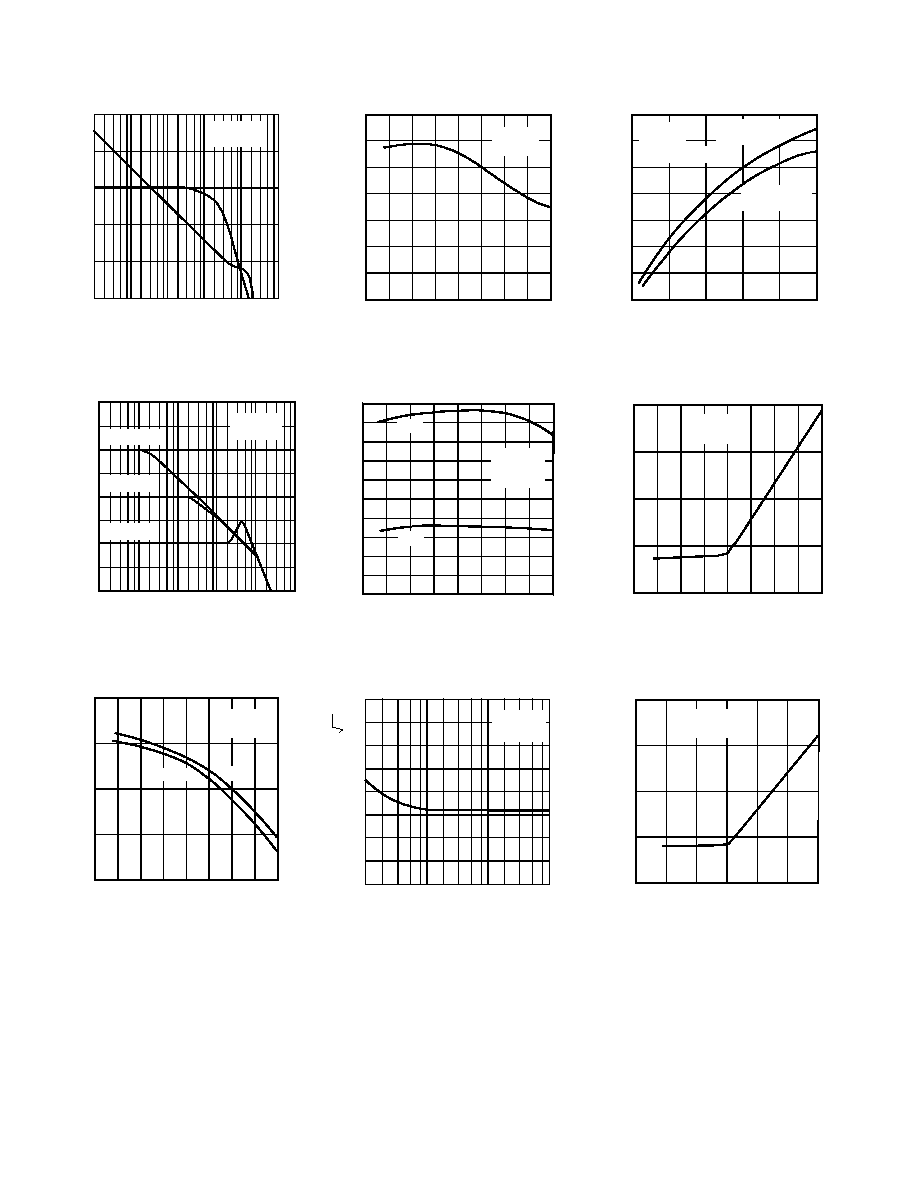
FREQUENCY ≠ Hz
1k
10k
100k
1M
100M
10M
0
40
20
80
60
OPEN-LOOP GAIN ≠ dB
PHASE ≠ Degrees
90
135
0
45
180
V
S
= ±15V
T
A
= +25
∞
C
Figure 5. Open-Loop Gain, Phase
vs. Frequency
FREQUENCY ≠ Hz
1M
1k
10k
100k
100M
10M
A = +100
VCL
A = +1
VCL
A = +10
VCL
CLOSED-LOOP GAIN ≠ dB
10
30
20
40
50
60
0
≠10
≠20
V
S
= ±15V
T
A
= +25
∞
C
Figure 6. Closed-Loop Gain vs.
Frequency
60
45
40
55
50
PHASE MARGIN ≠ Degrees
125
≠75
≠25
≠50
25
0
50
75
100
TEMPERATURE ≠ ∞C
V = ±15V
S
R
L
= 10k
GBW
ÿ
M
50
3.5
3.0
4.5
4.0
GAIN BANDWIDTH PRODUCT ≠ MH
Z
Figure 7. OP482 Phase Margin and
Gain Bandwidth Product vs.
Temperature
OVERSHOOT ≠ %
500
0
300
100
200
400
LOAD CAPACITANCE ≠ pF
70
10
0
60
50
40
30
20
A
VCL
= +1
NEGATIVE EDGE
L
POSITIVE EDGE
V
S
= ±15V
R
L
= 2k
V
IN
= 100mV p-p
A
VCL
= +1
Figure 11. Small Signal Overshoot
vs. Load Capacitance
1000
1.0
0.1
100
10
INPUT BIAS CURRENT ≠ pA
TEMPERATURE ≠ ∞C
125
≠25
≠50
25
0
50
75
100
V
CM
= 0
V
S
= ±15V
Figure 12. OP282 Input Bias Current
vs. Temperature
COMMON - MODE VOLTAGE ≠ V
15
≠15
0
5
10
≠10
≠5
T
A
= +25
∞
C
V
S
= ±15V
INPUT BIAS CURRENT ≠ pA
100
1
1000
0.1
10
Figure 13. OP282 Input Bias Current
vs. Common-Mode Voltage
125
≠75
≠25
≠50
25
0
50
75
100
TEMPERATURE ≠ ∞C
OPEN-LOOP GAIN ≠ V/MV
30
35
20
15
5
25
10
V = ±15V
S
R
L
= 10k
Figure 8. Open-Loop Gain (V/mV)
SLEW RATE ≠ V/µs
20
25
15
10
5
L
125
≠75
≠25
≠50
25
0
50
75
100
TEMPERATURE ≠∞C
≠ SR
+ SR
V
S
= ±15V
R
L
= 10k
C
L
= 50pF
Figure 9. OP282/OP482 Slew Rate
vs. Temperature
FREQUENCY ≠ Hz
10
100
1k
10k
80
0
20
10
40
30
50
60
70
VOLTAGE NOISE DENSITY ≠ nV/ Hz
V = ±15V
S
T = +25∞C
A
Figure 10. Voltage Noise Density
vs. Frequency

OP282/OP482
REV. B
≠9≠
SUPPLY VOLTAGE ≠ Volts
±15
0
±20
±10
±5
RELATIVE SUPPLY CURRENT ≠ ISY
1.10
0.90
1.15
0.85
1.00
1.05
0.95
T
A
= +25∞C
Figure 14. Relative Supply Current
vs. Supply Voltage
RELATIVE SUPPLY CURRENT ≠ ISY
TEMPERATURE ≠ ∞C
1.20
0.80
0.90
0.85
1.00
0.95
1.05
1.10
1.15
≠50
≠75
125
100
75
50
25
0
≠25
V
SUP
= ±15
Figure 15. Relative Supply Current
vs. Temperature
SHORT CIRCUIT CURRENT ≠ mA
20
15
5
10
V
S
= ±15V
SINK
SOURCE
TEMPERATURE ≠ ∞C
75
≠75
0
25
50
≠50
≠25
100 125
Figure 16. OP282/OP482 Short
Circuit Current vs. Temperature
SUPPLY VOLTAGE ≠ Volts
±15
0
±10
±5
±20
≠5
OUTPUT VOLTAGE SWING ≠ Volts
0
15
5
10
20
≠10
≠20
≠15
R
L
= 10k
T
A
= +25∞C
Figure 17. Output Voltage Swing
vs. Supply Voltage
LOAD RESISTANCE ≠
10k
1k
100
ABSOLUTE OUTPUT VOLTAGE ≠ Volts
16
0
2
8
6
10
12
14
4
T
A
= +25∞C
V
S
= ±15V
POSITIVE
SWING
NEGATIVE
SWING
Figure 18. Maximum Output Voltage
vs. Load Resistance
MAXIMUM OUTPUT SWING ≠ Volts
30
0
15
5
10
25
20
V
S
= ±15V
T
A
= +25∞C
R
L
= 10k
A
VCL
= +1
100k
10k
1k
1M
FREQUENCY ≠ Hz
Figure 19. Maximum Output Swing
vs. Frequency
IMPEDANCE ≠
600
0
300
100
200
500
400
V
S
= ±15V
T
A
= +25
∞
C
A = 1000
VCL
A = 100
VCL
A = +10
VCL
A = 1
VCL
1M
1k
100
100k
10k
FREQUENCY ≠ Hz
Figure 20. OP482 Closed-Loop Out-
put Impedance vs. Frequency
PSRR ≠ dB
100
≠20
40
0
20
80
60
1M
1k
100
100k
10k
T
A
= +25
∞
C
V
S
= ±15V
V = 100mV
FREQUENCY ≠ Hz
+ PSRR
≠ PSRR
Figure 21. OP282 Power Supply
Rejection Ratio (PSRR) vs. Frequency
CMRR ≠ dB
100
≠20
40
0
20
80
60
1M
1k
100
100k
10k
FREQUENCY ≠ Hz
T
A
= +25
∞
C
V = ±15V
S
V = 100mV
CM
Figure 22. OP282 Common-Mode
Rejection Ratio (CMRR) vs. Frequency
OP282/OP482
REV. B
≠10≠
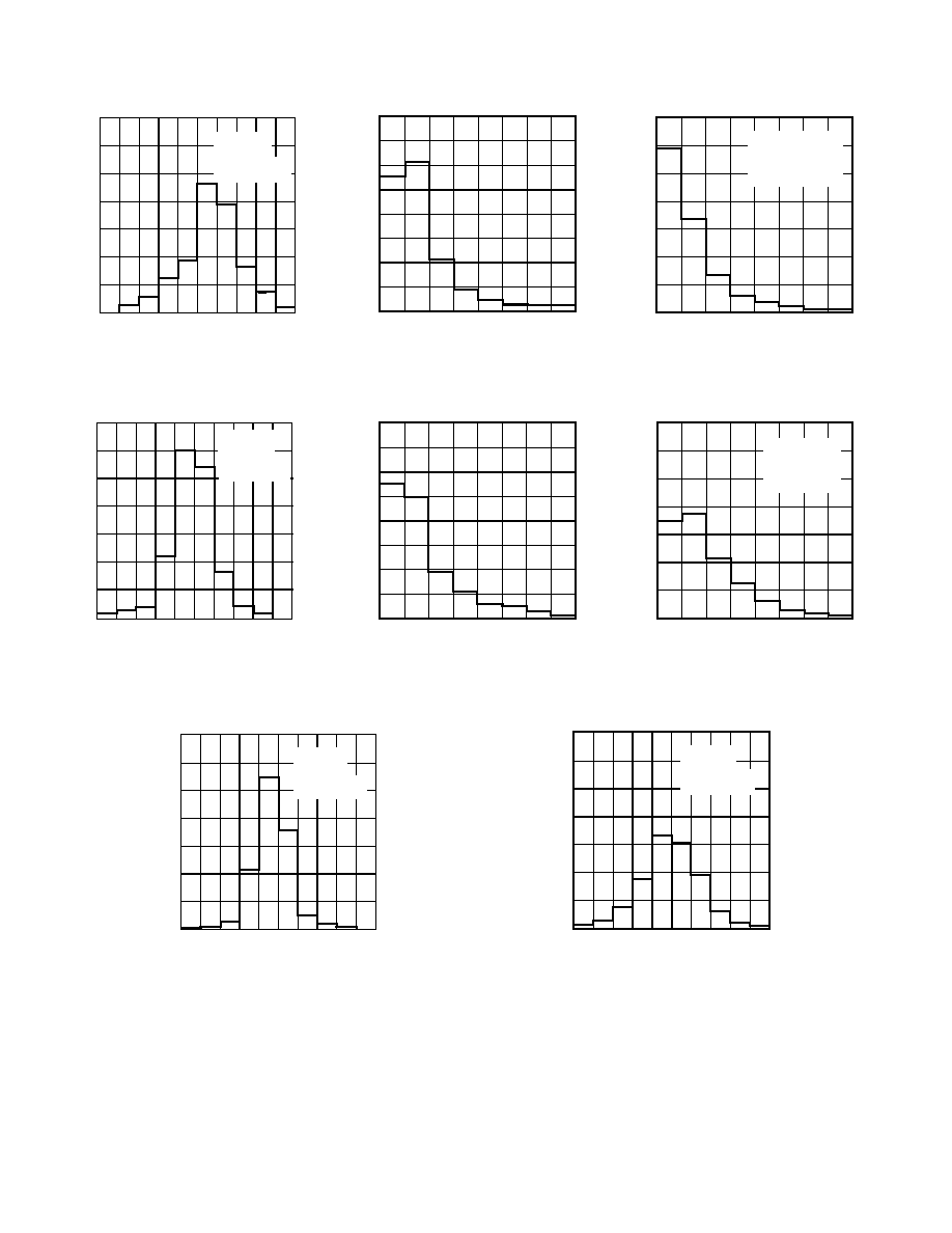
0
UNITS
280
120
40
80
240
160
200
2000
-1600
-2000
1600
1200
800
400
0
-400
-800
-1200
V ≠ µV
OS
V = ±15V
S
T = +25∞C
A
(630 OP
AMPS
)
315 OP282
◊
Figure 23. V
OS
Distribution "P"
Package
0
UNITS
280
120
40
80
240
160
200
2000
≠1600
≠2000
1600
1200
800
400
0
≠400
≠800
≠1200
V ≠ µV
OS
V
S
= ±15V
T
A
= +25
∞
C
(640 OP AMPS)
320 OP282
◊
Figure 24. V
OS
Distribution "Z"
Package
UNITS
0
600
700
300
100
200
400
500
32
4
0
28
24
20
16
12
8
TCV ≠ µV/∞C
OS
1200 OP AMPS
V
S
= ±15V
-40∞C T
A
+125
∞
C
300 OP482
◊
Figure 27. OP482 TCV
OS
Distribution
"Z" Package
UNITS
0
600
700
300
100
200
400
500
32
4
0
28
24
20
16
12
8
TCV ≠ µV/∞C
OS
1200 OP AMPS
V
S
= ±15V
-40∞C T
A
+85
∞
C
300 OP482
◊
Figure 28. TCV
OS
Distribution "P"
Package
UNITS
320
0
80
40
160
120
200
240
280
32
4
0
28
24
20
16
12
8
TCV ≠ µV/∞C
OS
Figure 25. OP282 TCV
OS
(
µ
V/
∞
C)
Distribution "P" Package
UNITS
320
0
80
40
160
120
200
240
280
32
4
0
28
24
20
16
12
8
TCV ≠ µV/∞C
OS
Figure 26. OP282 TCV
OS
(
µ
V/
∞
C)
Distribution "Z" Package
UNITS
0
600
700
300
100
200
400
500
2000
≠1600
≠2000
1600
1200
800
400
0
≠400
≠800
≠1200
V ≠ µV
OS
T
A
= +25
∞
C
V
S
= ±15V
1200 OP AMPS
300 OP482
Figure 30. OP482 V
OS
Distribution "P"
Package
V ≠ µV
OS
2000
≠1600
≠2000
1600
1200
800
400
0
≠400
≠800
≠1200
UNITS
0
600
700
300
100
200
400
500
T
A
= +25
∞
C
V
S
= ±15V
1200 OP AMPS
300 OP482
Figure 29. OP482 V
OS
Distribution "Z"
Package
OP282/OP482
REV. B
≠11≠
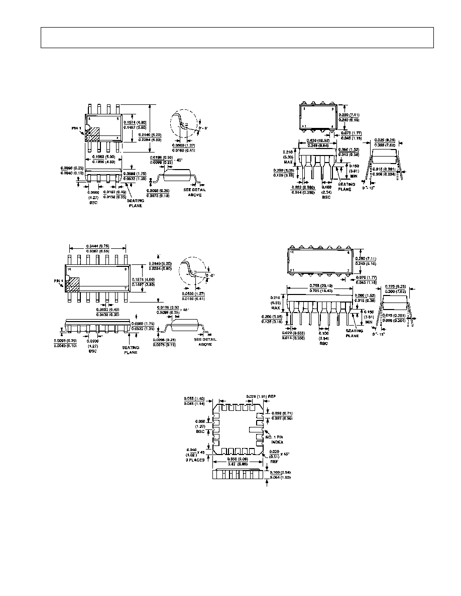
OUTLINE DIMENSIONS
Dimensions shown in inches and (mm).
8-Lead Narrow-Body SOIC
(S Suffix)
14-Lead Narrow-Body SOIC
(S Suffix)
8-Lead Epoxy DIP
(P Suffix)
14-Lead Epoxy DIP
(P Suffix)
20-Position Chip Carrier
(RC Suffix)

C1597≠24≠11/91
PRINTED IN U.S.A.
≠12≠
REV. B