 | ÐлекÑÑоннÑй компоненÑ: OP490A | СкаÑаÑÑ:  PDF PDF  ZIP ZIP |
OP490 Data sheet
REV. C
Information furnished by Analog Devices is believed to be accurate and
reliable. However, no responsibility is assumed by Analog Devices for its
use, nor for any infringements of patents or other rights of third parties
that may result from its use. No license is granted by implication or
otherwise under any patent or patent rights of Analog Devices.
a
OP490
One Technology Way, P.O. Box 9106, Norwood, MA 02062-9106, U.S.A.
Tel: 781/329-4700
www.analog.com
Fax: 781/326-8703
© Analog Devices, Inc., 2002
Low Voltage Micropower
Quad Operational Amplifier
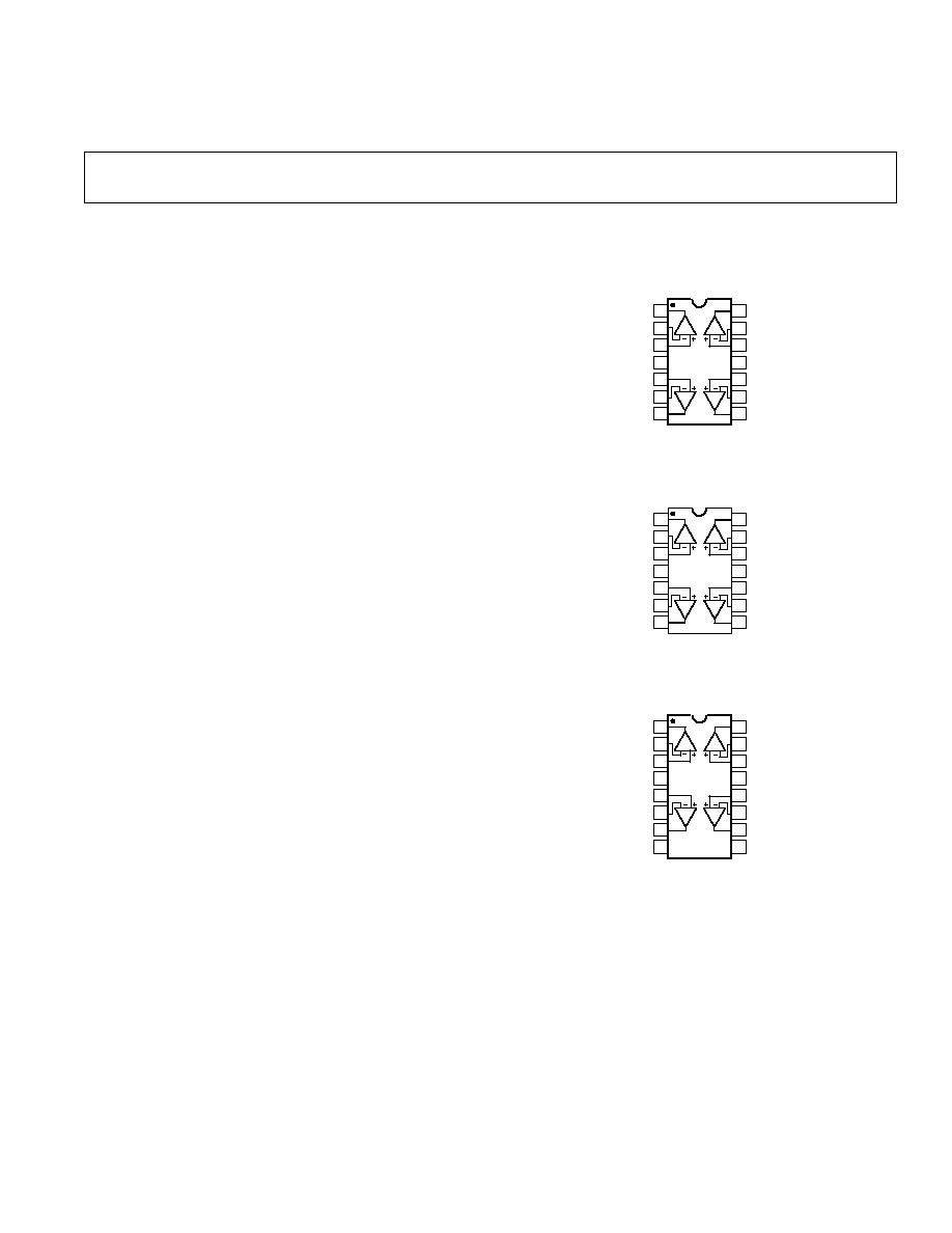
PIN CONNECTION
FEATURES
Single/Dual-Supply Operation
1.6 V to 36 V
0.8 V to 18 V
True Single-Supply Operation; Input and Output
Voltage Ranges Include Ground
Low Supply Current: 80 A Max
High Output Drive: 5 mA Min
Low Offset Voltage: 0.5 mA Max
High Open-Loop Gain: 700 V/mV Min
Outstanding PSRR: 5.6 mV/V Min
Industry Standard Quad Pinouts
Available in Die Form
GENERAL DESCRIPTION
The OP490 is a high-performance micropower quad op amp
that operates from a single supply of 1.6 V to 36 V or from
dual supplies of
±0.8 V to ±18 V. Input voltage range includes
the negative rail allowing the OP490 to accommodate input
signals down to ground in single-supply operation. The
OP490's output swing also includes ground when operating
from a single supply, enabling "zero-in, zero-out" operation.
The quad OP490 draws less than 20
mA of quiescent supply
current per amplifier, but each amplifier is able to deliver
over 5 mA of output current to a load. Input offset voltage is
under 0.5 mV with offset drift below 5
mV/C over the military
temperature range. Gain exceeds over 700,000 and CMR is
better than 100 dB. A PSRR of under 5.6
mV/V minimizes
offset voltage changes experienced in battery-powered systems.
The quad OP490 combines high performance with the space
and cost savings of quad amplifiers. The minimal voltage and
current requirements of the OP490 make it ideal for battery-
and solar-powered applications, such as portable instruments
and remote sensors.
14-Lead Hermetic DIP
(Y Suffix)
1
2
3
4
5
6
7
14
13
12
11
10
9
8
OUT A
IN A
+IN A
V+
+IN B
IN B
OUT B
IN D
+IN D
V
+IN C
IN C
OUT C
OUT D
14-Lead Plastic DIP
(P Suffix)
1
2
3
4
5
6
7
14
13
12
11
10
9
8
OUT A
IN A
+IN A
V+
+IN B
IN B
OUT B
IN D
+IN D
V
+IN C
IN C
OUT C
OUT D
16-Lead SOIC
(S Suffix)
1
2
3
4
5
6
7
8
14
13
12
11
10
9
15
16
OUT A
IN A
+IN A
V+
+IN B
IN B
OUT B
IN D
+IN D
V
+IN C
IN C
OUT C
OUT D
NC
NC
NC = NO CONNECT

REV. C
2
OP490SPECIFICATIONS
OP490E
OP490F
OP490G
Parameter
Symbol
Conditions
Min
Typ
Max
Min
Typ
Max
Min
Typ
Max
Unit
Input Offset
Voltage
V
OS
0.2
0.5
0.4
0.75
0.6
1.0
mV
Input Offset
Current
I
OS
V
CM
= 0 V
0.4
3.0
0.4
5
0.4
5
nA
Input Bias
Current
I
B
V
CM
= 0 V
4.2
15.0
4.2
20
4.2
25
nA
Large Signal
A
VO
V
S
=
±15 V, V
O
=
±10 V,
Voltage Gain
R
L
= 100 k
W
700
1,200
500
1,000
400
800
V/mV
R
L
= 10 k
W
350
600
250
500
200
400
V/mV
R
L
= 2 k
W
125
250
100
200
100
200
V/mV
V+ = 5 V, V = 0 V,
1 V < V
O
< 4 V
R
L
= 100 k
W
200
400
125
300
100
250
V/mV
R
L
= 10 k
W
100
180
75
140
70
140
V/mV
Input Voltage
IVR
V+ = 5 V, V = 0 V
0/4
0/4
0/4
V
Range
V
S
=
±15 V
1
15/+13.5
15/+13.5
15/+13.5
V
Output Voltage
V
O
V
S
=
±15 V, R
L
= 10 k
W
±13.5
±14.2
±13.5
±14.2
±13.5
±14.2
V
Swing
R
L
= 2 k
W
±10.5
±11.5
±10.5
±11.5
±10.5
±11.5
V
V
OH
V+ = 5 V, V = 0 V,
R
L
= 2 k
W
4.0
4.2
4.0
4.2
4.0
4.2
V
V
OL
V+ = 5 V, V = 0 V,
R
L
= 10 k
W
100
500
100
500
100
500
mV
Common-Mode
CMRR
V+ = 5 V, V = 0 V,
90
110
80
100
800
100
dB
Rejection Ratio
0 V < V
CM
< 4 V
V
S
=
±15 V,
100
130
90
120
90
120
dB
15 V < V
CM
< +13.5 V
Power Supply
Rejection Ratio
PSRR
1.0
5.6
3.2
10
3.2
10
mV/V
Slew Rate
SR
V
S
=
±15 V
5
12
5
12
5
12
V/ms
Supply Current
V
S
=
±1.5 V, No Load
40
60
40
60
40
60
mA
(All Amplifiers)
I
SY
V
S
=
±15 V, No Load
60
80
60
80
60
80
mA
Capacitive Load
A
V
= 1
650
650
650
pF
Stability
Input Noise
e
n
p-p
f
O
= 0.1 Hz to 10 Hz,
Voltage
V
S
=
±15 V
3
3
3
mV p-p
Input Resistance
Differential Mode
R
IN
V
S
=
±15 V
30
30
30
M
W
Input Resistance
Common-Mode
R
INCM
V
S
=
±15 V
20
20
20
G
W
Gain Bandwidth
Product
GBWP
A
V
= 1
20
20
20
kHz
Channel Separation
CS
f
O
= 10 Hz, V
O
= 20 V p-p
120
150
120
150
120
150
dB
V
S
=
±15 V
2
NOTES
1
Guaranteed by CMRR test.
2
Guaranteed but not 100% tested.
Specifications subject to change without notice
ELECTRICAL CHARACTERISTICS
(@ V
S
= 1.5 V to 15 V, T
A
= 25 C, unless otherwise noted)

REV. C
3
OP490
(@ V
S
= 1.5 V to 15 V, 25 C
£
T
A
£
+85 C for OP490E/F, 40 C
£
T
A
£
+125 C for
OP490G, unless otherwise noted)
OP490E
OP490F
OP490G
Parameter
Symbol
Conditions
Min
Typ
Max
Min
Typ
Max
Min
Typ
Max
Unit
Input Offset
Voltage
V
OS
0.32
0.8
0.6
1.35
0.8
1.5
mV
Average Input
Offset Voltage Drift
TCV
OS
V
S
=
±15 V
2
5
4
4
mV/C
Input Offset
Current
I
OS
V
CM
= 0 V
0.8
3
1.0
5
1.3
7
nA
Input Bias
Current
I
B
V
CM
= 0 V
4.4
15
4.4
20
4.4
25
nA
Large Signal
A
VO
V
S
=
±15 V, V
O
=
±10 V,
Voltage Gain
R
L
= 100 k
W
500
800
350
700
300
600
V/mV
R
L
= 10 k
W
250
400
175
250
150
250
V/mV
R
L
= 2 k
W
100
200
75
150
75
125
V/mV
V+ = 5 V, V = 0 V,
1 V < V
O
< 4 V
R
L
= 100 k
W
150
280
100
220
80
160
V/mV
R
L
= 10 k
W
75
140
50
110
40
90
V/mV
Input Voltage
IVR
V+ = 5 V, V = 0 V
0.3/5
0.3/5
0.3/5
V
Range
V
S
=
±15 V
*
15/+13.5
15/+13.5
15/+13.5
V
Output Voltage
V
O
V
S
=
±15 V, R
L
= 10 k
W
±13
±14
±13
±14
±13
±14
V
Swing
R
L
= 2 k
W
±10
±11
±10
±11
±10
±11
V
V
OH
V+ = 5 V, V = 0 V,
R
L
= 2 k
W
3.9
4.1
3.9
4.1
3.9
4.1
V
V
OL
V+ = 5 V, V = 0 V,
R
L
= 10 k
W
100
500
100
500
100
500
mV
Common-Mode
CMRR
V+ = 5 V, V = 0 V,
90
110
80
100
800
100
dB
Rejection Ratio
0 V < V
CM
< 3.5 V
V
S
=
±15 V,
100
120
90
110
90
110
dB
15 V < V
CM
< +13.5 V
Power Supply
Rejection Ratio
PSRR
1.0
5.6
3.2
10
5.6
17.8
mV/V
Supply Current
V
S
=
±1.5 V, No Load
65
100
65
100
60
100
mA
(All Amplifiers)
I
SY
V
S
=
±15 V, No Load
80
120
80
120
75
120
mA
NOTE
*Guaranteed by CMRR test.
Specifications subject to change without notice
ELECTRICAL CHARACTERISTICS
REV. C
OP490
4
+IN
IN
OUTPUT
V+
V
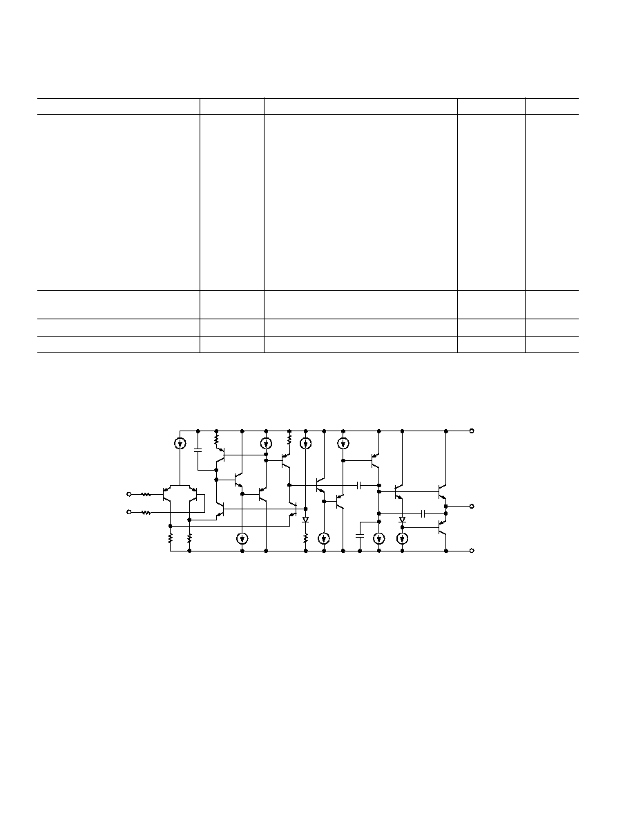
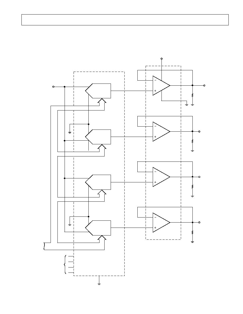
Figure 1. Simplified Schematic
Parameter
Symbol
Conditions
Limits
Unit
Input Offset Voltage
V
OS
0.75
mV max
Input Offset Current
I
OS
V
CM
= 0 V
5
nA max
Input Bias Current
I
B
V
CM
= 0 V
20
nA max
Large Signal Voltage Gain
A
VO
V
S
=
±15 V, V
O
=
±10 V,
R
L
= 100 k
W
500
V/mV min
R
L
= 10 k
W
250
V/mV min
V+ = 5 V, V = 0 V
125
V/mV min
1 V < V
O
< 4 V, R
L
= 100 k
W
Input Voltage Range
IVR
V+ = 5 V, V = 0 V
0/4
V min
V
S
=
±15 V*
15/+13.5
V min
Output Voltage Swing
V
O
V
S
=
±15 V
R
L
= 10 k
W
±13.5
V min
R
L
= 2 k
W
±10.5
V min
V
OH
V+ = 5 V, V = 0 V, R
L
= 2 k
W
4.0
V min
V
OL
V+ = 5 V, V = 0 V, R
L
= 10 k
W
500
mV max
Common-Mode Rejection Ratio
CMRR
V+ = 5 V, V = 0 V, 0 V < V
CM
< 4 V
80
dB min
V
S
=
±15 V, 15 V < V
CM
< +13.5 V
90
dB min
Power Supply Rejection Ratio
PSRR
10
mV/V max
Supply Current (All Amplifiers)
I
SY
V
S
=
±15 V, No Load
80
mA max
NOTE
*Guaranteed by CMRR test.
Electrical tests are performed at wafer probe to the limits shown. Due to variations in assembly methods and normal yield loss, yield after packaging is not guaranteed
for standard product dice. Consult factory to negotiate specifications based on dice lot qualifications through sample lot assembly and testing.
WAFER TEST LIMITS
(@ V
S
= 1.5 V to 15 V, T
A
= 25 C, unless otherwise noted)
REV. C
OP490
5
ABSOLUTE MAXIMUM RATINGS
*
Supply Voltage . . . . . . . . . . . . . . . . . . . . . . . . . . . . . . . .
±18 V
Digital Input Voltage . . . . . . . . [(V) 20 V] to [(V+) + 20 V]
Common-Mode Input Voltage [(V) 20 V] to [(V+) + 20 V]
Output Short Circuit Duration . . . . . . . . . . . . . . . Continuous
Storage Temperature Range
Y and P Packages . . . . . . . . . . . . . . . . . . . 65
C to +150C
Operating Temperature Range
OP490E, OP490F . . . . . . . . . . . . . . . . . . . 25
C to +85C
OP490G . . . . . . . . . . . . . . . . . . . . . . . . . . . 40
C to +85C
Junction Temperature (T
J
) . . . . . . . . . . . . . 65
C to +150C
Lead Temperature Range (Soldering, 60 sec) . . . . . . . . 300
C
*Stresses above those listed under Absolute Maximum Ratings may cause perma-
nent damage to the device. This is a stress rating only; functional operation of the
device at these or any other conditions above those listed in the operational
sections of this specification is not implied. Exposure to absolute maximum rating
conditions for extended periods may affect device reliability.
Package Type
JA
*
JC
Unit
14-Pin Hermetic DIP (Y)
99
12
C/W
14-Pin Plastic DIP (P)
76
33
C/W
16-Pin SOL (S)
92
27
C/W
*
q
JA
is specified for worst case mounting conditions, i.e.,
q
JA
is specified for
device in socket for CERDIP and PDIP packages;
q
JA
is specified for device
soldered to printed circuit board for SOL package
CAUTION
ESD (electrostatic discharge) sensitive device. Electrostatic charges as high as 4000 V readily
accumulate on the human body and test equipment and can discharge without detection. Although
the OP490 features proprietary ESD protection circuitry, permanent damage may occur on devices
subjected to high-energy electrostatic discharges. Therefore, proper ESD precautions are
recommended to avoid performance degradation or loss of functionality.
WARNING!
ESD SENSITIVE DEVICE
SMD Part Number
ADI Equivalent
5962-89670013A
*
OP490ATCMDA
5962-8967001CA
*
OP490AYMDA
*Not recommended for new designs. Obsolete April 2002.
ORDERING GUIDE
Temperature
Package
Package
Model
Range
Description
Option
OP490EY
*
25
C to +85C 14-Lead CERDIP
Y-14
OP490FY
*
25
C to +85C 14-Lead CERDIP
Y-14
OP490GP
40
C to +85C 14-Lead Plastic DIP P-14
OP490GS
40
C to +85C 16-Lead SOIC
S-14
*Not recommended for new designs. Obsolete April 2002.
For Military processed devices, please refer to the Standard
Microcircuit Drawing (SMD) available at
www.dscc.dla.mil/programs/milspec/default.asp
REV. C
OP490
6
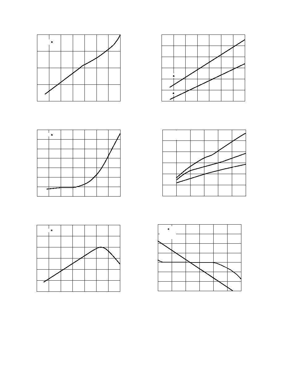
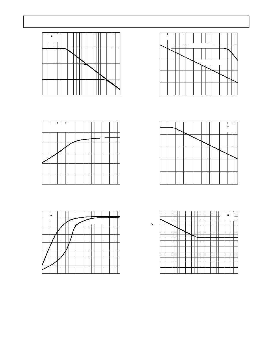
TEMPERATURE C
0
INPUT OFFSET
V
OL
T
A
GE mV
0.3
0.2
0.1
75
125
50
25
0
25
50
0.4
V
S
= 15V
75
TPC 1. Input Offset Voltage vs. Temperature
TEMPERATURE C
0.2
INPUT OFFSET CURRENT nA
1.0
0.8
0.6
0.4
1.4
1.2
75
125
50
25
0
25
50
1.6
V
S
= 15V
75
TPC 2. Input Offset Current vs. Temperature
TEMPERATURE C
3.6
INPUT BIAS CURRENT nA
4.4
4.2
4.0
3.8
4.6
75
125
50
25
0
25
50
4.8
V
S
= 15V
75
TPC 3. Input Bias Current vs. Temperature
TEMPERATURE C
30
TO
TA
L SUPPL
Y CURRENT
A
70
60
50
40
80
75
125
50
25
0
25
50
90
V
S
= 15V
V
S
= 1.5V
75
TPC 4. Total Supply Current vs. Temperature
SINGLE-SUPPLY VOLTAGE V
600
0
0
30
5
OPEN-LOOP GAIN
V/mV
10
15
20
25
500
400
300
200
100
T
A
= 25 C
R
L
= 10k
25 C
85 C
125 C
TPC 5. Open-Loop Gain vs. Single-Supply Voltage
FREQUENCY Hz
140
0
0.1
100k
1
OPEN-LOOP GAIN
dB
10
100
1k
10k
120
100
80
40
20
60
V
S
= 15V
T
A
= 25 C
R
L
= 10k
0
45
135
180
90
PHASE SHIFT Degrees
GAIN
TPC 6. Open-Loop Gain and Phase Shift vs. Frequency
Typical Performance Characteristics
REV. C
7
OP490
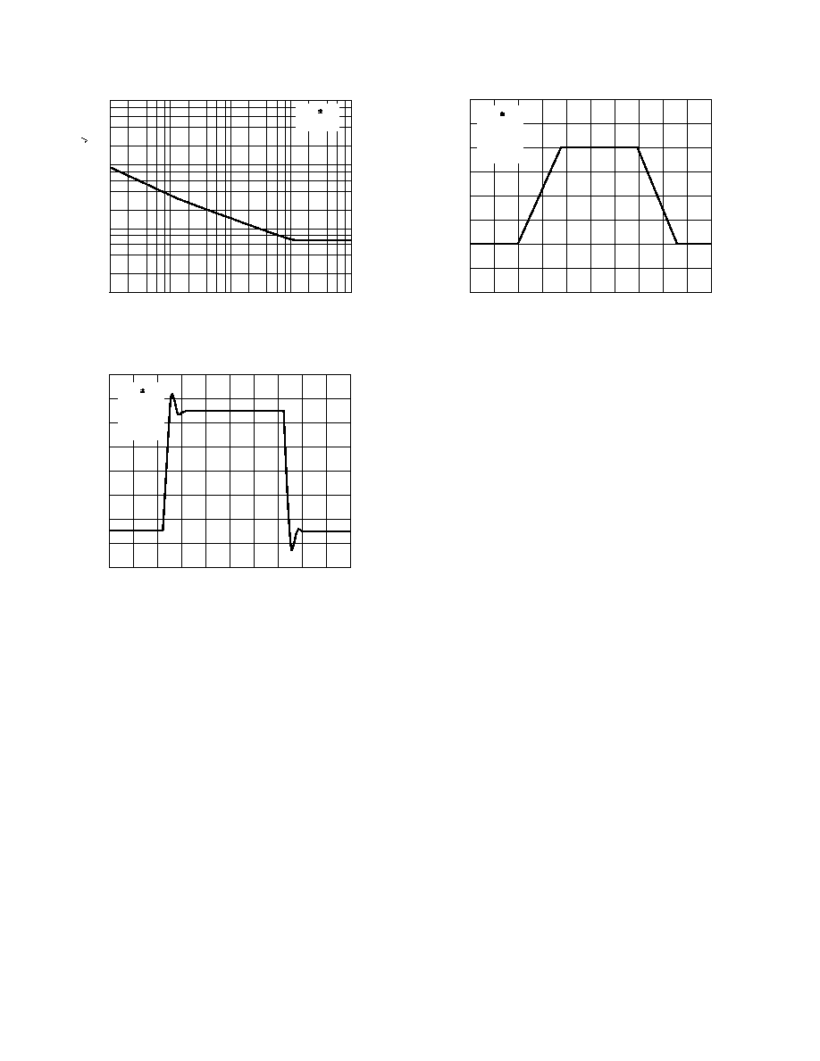
FREQUENCY Hz
60
40
20
10
100k
100
CLOSED-LOOP GAIN dB
1k
10k
20
0
V
S
= 15V
T
A
= 25 C
TPC 7. Closed-Loop Gain vs. Frequency
LOAD RESISTANCE
6
5
0
100
100k
1k
OUTPUT
V
OL
T
A
GE SWING
V
10k
3
2
1
4
V+ = 5V, V = 0V
T
A
= 25 C
TPC 8. Output Voltage Swing vs. Load Resistance
LOAD RESISTANCE
16
14
0
100
100k
1k
OUTPUT SWING
V
10k
10
6
2
12
V
S
= 15
T
A
= 25 C
8
4
POSITIVE
NEGATIVE
TPC 9. Output Voltage Swing vs. Load Resistance
LOAD RESISTANCE
120
20
1
1k
10
PO
WER SUPPL
Y REJECTION dB
100
80
40
T
A
= 25 C
100
60
POSITIVE SUPPLY
NEGATIVE SUPPLY
TPC 10. Power Supply Rejection vs. Frequency
FREQUENCY Hz
140
0.1
1k
COMMON-MODE REJECTION dB
80
1
10
100
120
40
V
S
= 15V
T
A
= 25 C
100
60
TPC 11. Common-Mode Rejection vs. Frequency
VO
LTA
GE NOISE DENSITY nV/
Hz
FREQUENCY Hz
1k
100
1
0.1
1k
1
10
100
10
V
S
= 15V
T
A
= 25 C
TPC 12. Noise Voltage Density vs. Frequency
REV. C
OP490
8
VO
LTA
GE NOISE DENSITY nV/
Hz
FREQUENCY Hz
100
10
0.1
0.1
1k
1
10
100
1
V
S
= 15V
T
A
= 25 C
TPC 13. Current Noise Density vs. Frequency
TIME 100 s/DIV
0
0
0
0
0
0
VO
LTA
G
E
20mV/DIV
0
0
0
0
0
0
0
0
0
0
0
0
0
0
V
S
= 15V
T
A
= 25 C
A
V
= 1
R
L
= 10k
C
L
= 500pF
TPC 14. Small-Signal Transient Response
TIME 1ms/DIV
0
0
0
0
0
0
VO
LTA
G
E
5V/DIV
0
0
0
0
0
0
0
0
0
0
0
0
0
0
V
S
= 15V
T
A
= 25 C
A
V
= 1
R
L
= 10k
C
L
= 500pF
TPC 15. Large-Signal Transient Response
REV. C
OP490
9
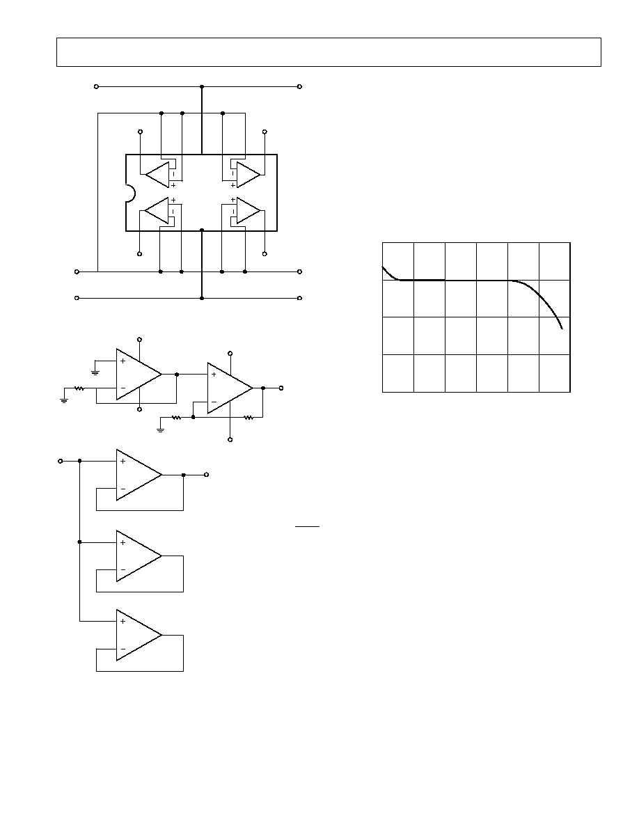
1
2
3
4
5
6
7
14
13
12
11
10
9
8
18V
+18V
GND
C
B
D
A
Figure 2. Burn-In Circuit
+15V
15V
1k
+15V
15V
V2
100
10k
1/4
OP490A
1/4
OP490B
OP37A
V1
V
IN
1/4
OP490C
1/4
OP490D
20V p-p @ 10Hz
CHANNEL SEPARATION = 20 LOG
V1
V2/1000
Figure 3. Channel Separation Test Circuit
APPLICATIONS INFORMATION
Battery-Powered Applications
The OP490 can be operated on a minimum supply voltage of
1.6 V, or with dual supplies of
±0.8 V, and draws only 60 mA of
supply current. In many battery-powered circuits, the OP490
can be continuously operated for hundreds of hours before
requiring battery replacement, reducing equipment downtime,
and operating costs.
High performance portable equipment and instruments fre-
quently use lithium cells because of their long shelf-life, light
weight, and high energy density relative to older primary cells.
Most lithium cells have a nominal output voltage of 3 V and are
noted for a flat discharge characteristic. The low supply current
HOURS
4
3
0
0
1750
250
LITHIUM-SULPHUR DIO
XIDE CELL
V
OL
T
A
GE
V
500
750
2
1
1000
1500
Figure 4. Lithium-Sulphur Dioxide Cell Discharge Charac-
teristic with OP490 and 100 k
W Loads
requirement of the OP490, combined with the flat discharge
characteristic of the lithium cell, indicates that the OP490 can
be operated over the entire useful life of the cell. Figure 4 shows
the typical discharge characteristic of a 1 Ah lithium cell power-
ing an OP490 with each amplifier, in turn, driving full output
swing into a 100 k
W load.
Single-Supply Output Voltage Range
In single-supply operation the OP490's input and output ranges
include ground. This allows true "zero-in, zero-out" operation.
The output stage provides an active pull-down to around 0.8 V
above ground. Below this level, a load resistance of up to 1 M
W
to ground is required to pull the output down to zero.
In the region from ground to 0.8 V, the OP490 has voltage gain
equal to the data sheet specification. Output current source
capability is maintained over the entire voltage range including
ground.
Input Voltage Protection
The OP490 uses a PNP input stage with protection resistors in
series with the inverting and noninverting inputs. The high
breakdown of the PNP transistors coupled with the protection
resistors provides a large amount of input protection, allowing
the inputs to be taken 20 V beyond either supply without dam-
aging the amplifier.
REV. C
OP490
10
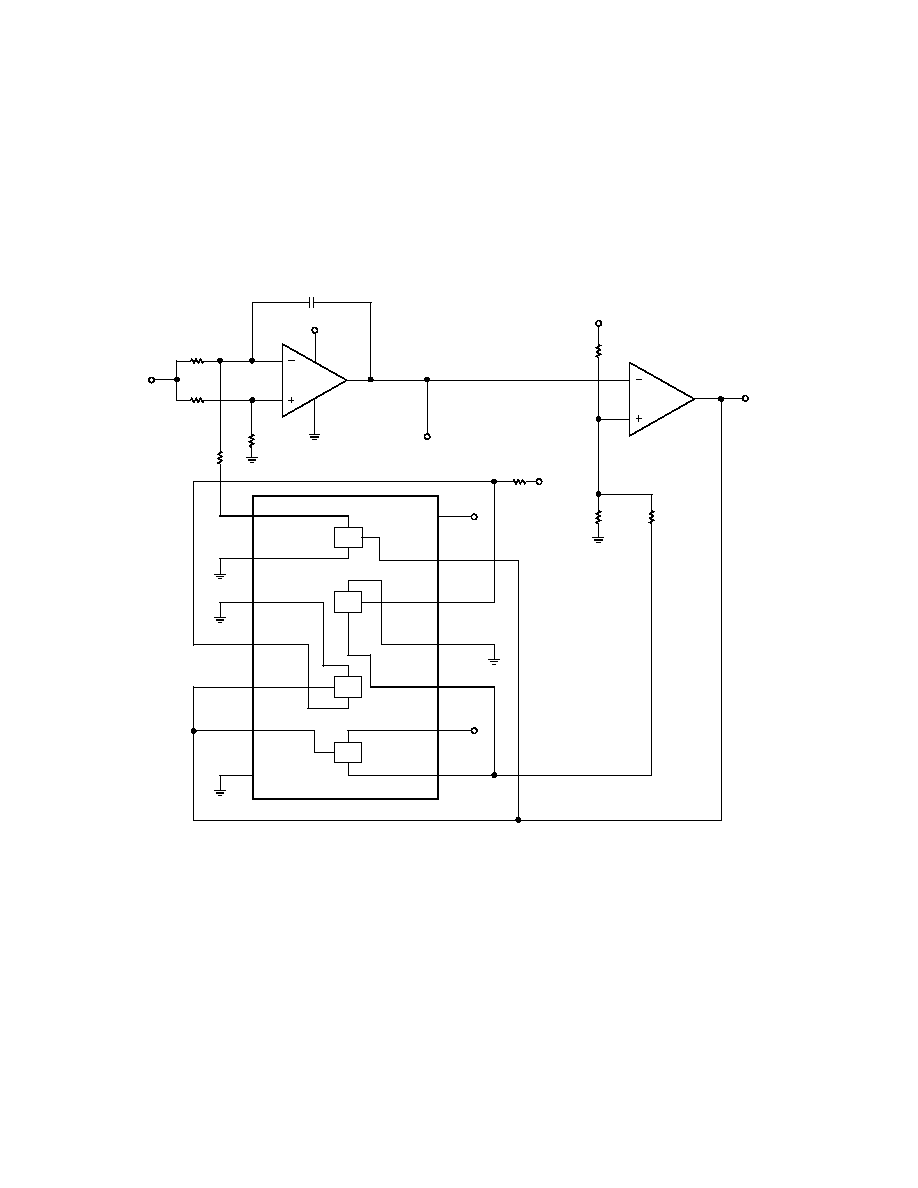
Micropower Voltage-Controlled Oscillator
An OP490 in combination with an inexpensive quad CMOS
switch comprise the precision V
CO
of Figure 5. This circuit
provides triangle and square wave outputs and draws only 75
mA
from a 5 V supply. A acts as an integrator; S1 switches the
charging current symmetrically to yield positive and negative
ramps. The integrator is bounded by B which acts as a Schmitt
trigger with a precise hysteresis of 1.67 V, set by resistors R5,
R6, and R7, and associated CMOS switches. The resulting
1
14
2
13
3
12
4
11
5
10
6
9
7
8
S3
S4
S2
S1
CONT
IN/OUT
CONT
OUT/IN
OUT/IN
IN/OUT
IN/OUT
OUT/IN
IN/OUT
OUT/IN
CONT
CONT
V
SS
V
DD
+5V
+5V
1/4
OP490E
A
+5V
R2
200k
V
CONTROL
R1
200k
R3
100k
R4
200k
11
4
2
3
1
TRIANGLE
OUT
+5V
R8
200k
6
5
7
+5V
R5
200k
SQUARE
OUT
R6
200k
R7
200k
C1
75nF
1/4
OP490E
B
Figure 5. Micropower Voltage Controlled Oscillator
output of A is a triangle wave with upper and lower levels of
3.33 V and 1.67 V. The output of B is a square wave with almost
rail-to-rail swing. With the components shown, frequency of
operation is given by the equation:
f
V
Volts
Hz V
OUT
CONTROL
=
( )
¥10
/
but this is easily changed by varying C1. The circuit operates
well up to a few hundred hertz.
REV. C
OP490
11
10
21
12
27
5
8
1/4
OP490E
A
+5V
R1
100k
11
4
2
V
REF
A
1
V
OUT
A
DAC A
1/4
DAC8408
1/4
OP490E
B
R2
100k
6
7
V
OUT
B
DAC B
1/4
DAC8408
V
REF
B
1/4
OP490E
C
R3
100k
13
14
V
OUT
C
DAC C
1/4
DAC8408
V
REF
C
1/4
OP490E
D
R4
100k
9
8
V
OUT
D
DAC D
1/4
DAC8408
V
REF
D
I
OUT2A/2B
I
OUT1A
I
OUT2C/2D
I
OUT1B
I
OUT1C
DAC DATA BUS
PIN9(LSB) 16(MSB)
2
2
REFERENCE
VOLTAGE
1.5V
21
25
5
4
6
24
23
I
OUT1D
OP490EY
DAC8408ET
A/B
17
R/W
18
DS1
19
20
DS2
DIGITAL
CONTROL
SIGNALS
28
DGND
Figure 6. Micropower Single-Supply Quad Voltage Output 8-Bit DAC
Micropower Single-Supply Quad Voltage-Output 8-Bit DAC
The circuit of Figure 6 uses the DAC8408 CMOS quad 8-bit
DAC, and the OP490 to form a single-supply quad voltage-output
DAC with a supply drain of only 140
mA. The DAC8408 is used
in voltage switching mode and each DAC has an output resistance
(
ª10 kW) independent of the digital input code. The output
amplifiers act as buffers to avoid loading the DACs. The 100 k
W
resistors ensure that the OP490 outputs will swing below 0.8 V
when required.
REV. C
OP490
12
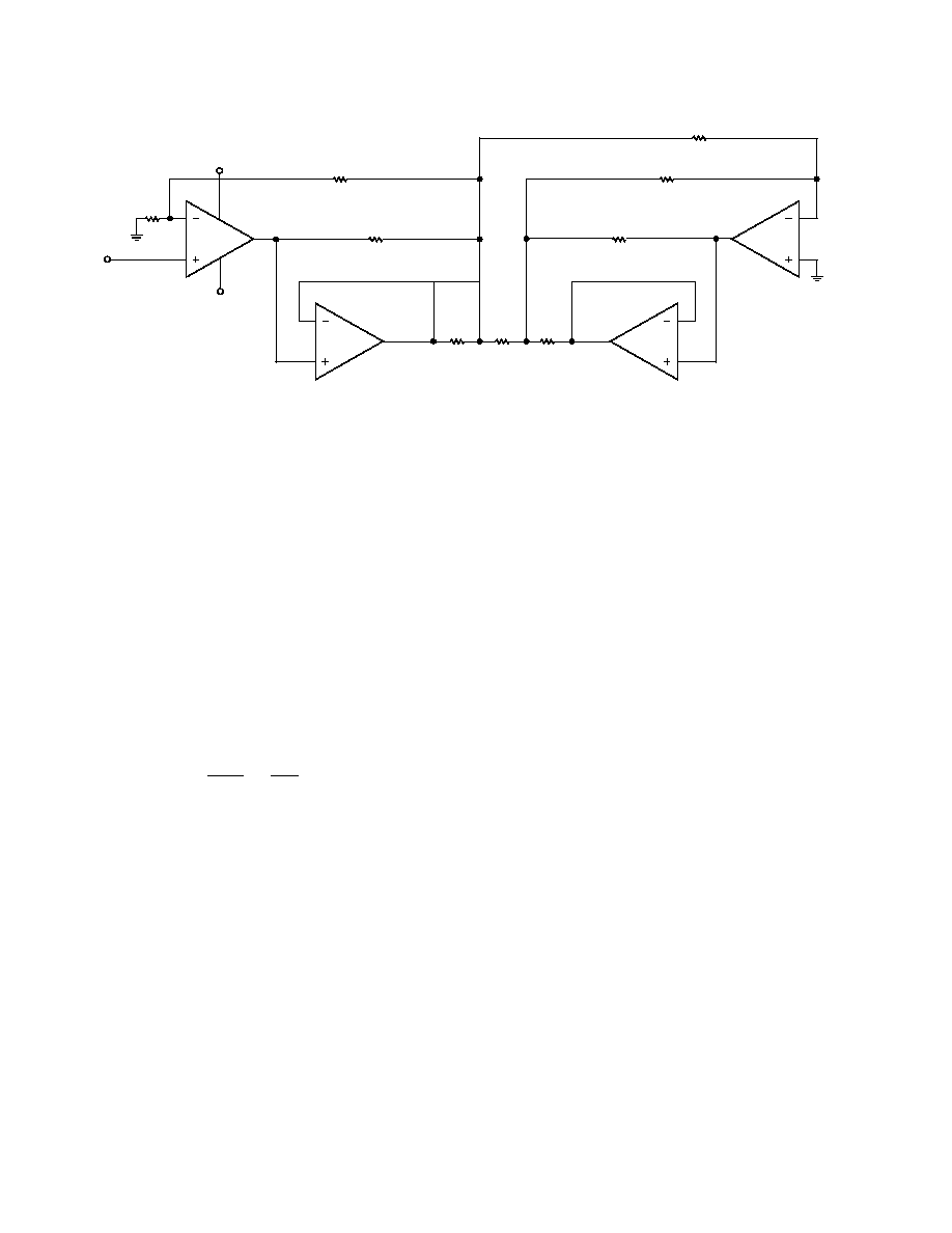
High Output Amplifier
The amplifier shown in Figure 7 is capable of driving 25 V p-p
into a 1 k
W load. Design of the amplifier is based on a bridge
configuration. A amplifies the input signal and drives the load
with the help of B. Amplifier C is a unity-gain inverter which
drives the load with help from D. Gain of the high output amplifier
with the component values shown is 10, but can easily be changed
by varying R1 or R2.
Single-Supply Micropower Quad Programmable Gain Amplifier
The combination of quad OP490 and the DAC8408 quad 8-bit
CMOS DAC, creates a quad programmable-gain amplifier with
a quiescent supply drain of only 140
mA. The digital code present
at the DAC, which is easily set by a microprocessor, determines
the ratio between the fixed DAC feedback resistor and the resis-
tance of the DAC ladder presents to the op amp feedback loop.
Gain of each amplifier is:
V
V
n
OUT
IN
= -
256
+15V
15V
1/4
OP490E
B
R1
1k
V
IN
2
3
11
4
1
R2
9k
1/4
OP490E
B
6
5
7
R3
50
R4
50
R
L
R8
50
8
1/4
OP490E
C
13
12
9
10
1/4
OP490E
D
R6
5k
R7
50
R5
5k
14
Figure 7. High Output Amplifier
where n equals the decimal equivalent of the 8-bit digital code
present at the DAC. If the digital code present at the DAC
consists of all zeros, the feedback loop will be open causing the
op amp output to saturate. The 10 M
W resistors placed in paral-
lel with the DAC feedback loop eliminates this problem with a
very small reduction in gain accuracy. The 2.5 V reference biases
the amplifiers to the center of the linear region providing maximum
output swing.
REV. C
OP490
13
DAC DATA BUS
PIN9(LSB) 16(MSB)
DAC8408ET
A/B
17
R/W
18
DS1
19
20
DS2
DIGITAL
CONTROL
SIGNALS
28
DGND
OP490EY
1/4
OP490E
D
13
14
V
OUT
D
DAC D
1/4
DAC8408
12
23
R4
10M
I
OUT1D
C4
0.1 F
+2.5V
REFERENCE
VOLTAGE
1/4
OP490E
A
11
4
2
V
REF
A
1
DAC A
1/4
DAC8408
3
2
3
+5V
4
1
R1
10M
V
DD
I
OUT1A
R
FB
A
1/4
OP490E
B
6
V
REF
B
7
V
OUT
B
DAC B
1/4
DAC8408
5
8
6
R2
10M
I
OUT1B
R
FB
B
5
I
OUT2A/2B
V
OUT
A
C1
0.1 F
C2
0.1 F
1/4
OP490E
C
9
V
REF
C
8
DAC C
1/4
DAC8408
10
27
25
R3
10M
I
OUT1C
R
FB
C
V
REF
D 21
V
IN
D
R
FB
D
24
I
OUT2C/2D
V
OUT
C
C3
0.1 F
V
IN
C
V
IN
B
V
IN
A
7
25
22
Figure 8. Single-Supply Micropower Quad Programmable Gain Amplifier
REV. C
OP490
14
14-Lead Hermetic DIP
(Y Suffix)
14
1
7
8
0.310 (7.87)
0.220 (5.59)
PIN 1
0.005 (0.13) MIN 0.098 (2.49) MAX
0.100 (2.54) BSC
15
0
0.320 (8.13)
0.290 (7.37)
0.015 (0.38)
0.008 (0.20)
SEATING
PLANE
0.200 (5.08)
MAX
0.785 (19.94) MAX
0.150
(3.81)
MIN
0.200 (5.08)
0.125 (3.18)
0.023 (0.58)
0.014 (0.36)
0.070 (1.78)
0.030 (0.76)
0.060 (1.52)
0.015 (0.38)
OUTLINE DIMENSIONS
Dimensions shown in inches and (mm).
Revision History
Location
Page
Data Sheet changed from REV. B to REV. C.
Deleted 28-Pin LCC (TC-Suffix) PIN CONNECTION DIAGRAM . . . . . . . . . . . . . . . . . . . . . . . . . . . . . . . . . . . . . . . . . . . . . . . . 1
Deleted ELECTRICAL CHARACTERISTICS . . . . . . . . . . . . . . . . . . . . . . . . . . . . . . . . . . . . . . . . . . . . . . . . . . . . . . . . . . . . . . . . 3
Edits to ABSOLUTE MAXIMUM RATINGS . . . . . . . . . . . . . . . . . . . . . . . . . . . . . . . . . . . . . . . . . . . . . . . . . . . . . . . . . . . . . . . . . 5
Edits to ORDERING GUIDE . . . . . . . . . . . . . . . . . . . . . . . . . . . . . . . . . . . . . . . . . . . . . . . . . . . . . . . . . . . . . . . . . . . . . . . . . . . . . . 5
14-Lead Plastic DIP
(P Suffix)
14
1
7
8
PIN 1
0.795 (20.19)
0.725 (18.42)
0.280 (7.11)
0.240 (6.10)
0.100 (2.54)
BSC
SEATING
PLANE
0.060 (1.52)
0.015 (0.38)
0.210 (5.33)
MAX
0.022 (0.558)
0.014 (0.356)
0.160 (4.06)
0.115 (2.93)
0.070 (1.77)
0.045 (1.15)
0.130
(3.30)
MIN
0.195 (4.95)
0.115 (2.93)
0.015 (0.381)
0.008 (0.204)
0.325 (8.25)
0.300 (7.62)
16-Lead SOIC
(S Suffix)
SEATING
PLANE
0.0118 (0.30)
0.0040 (0.10)
0.0192 (0.49)
0.0138 (0.35)
0.1043 (2.65)
0.0926 (2.35)
0.050 (1.27)
BSC
16
9
8
1
0.4193 (10.65)
0.3937 (10.00)
0.2992 (7.60)
0.2914 (7.40)
PIN 1
0.4133 (10.50)
0.3977 (10.00)
0.0125 (0.32)
0.0091 (0.23)
8
0
0.0291 (0.74)
0.0098 (0.25)
45
0.0500 (1.27)
0.0157 (0.40)

15

16
PRINTED IN U.S.A.
C0030804/02(C)