 | –≠–ª–µ–∫—Ç—Ä–æ–Ω–Ω—ã–π –∫–æ–º–ø–æ–Ω–µ–Ω—Ç: OP777 | –°–∫–∞—á–∞—Ç—å:  PDF PDF  ZIP ZIP |
REV. 0
Information furnished by Analog Devices is believed to be accurate and
reliable. However, no responsibility is assumed by Analog Devices for its
use, nor for any infringements of patents or other rights of third parties
which may result from its use. No license is granted by implication or
otherwise under any patent or patent rights of Analog Devices.
a
OP777
One Technology Way, P.O. Box 9106, Norwood, MA 02062-9106, U.S.A.
Tel: 781/329-4700
World Wide Web Site: http://www.analog.com
Fax: 781/326-8703
© Analog Devices, Inc., 2000
Precision Micropower
Single Supply
Operational Amplifier
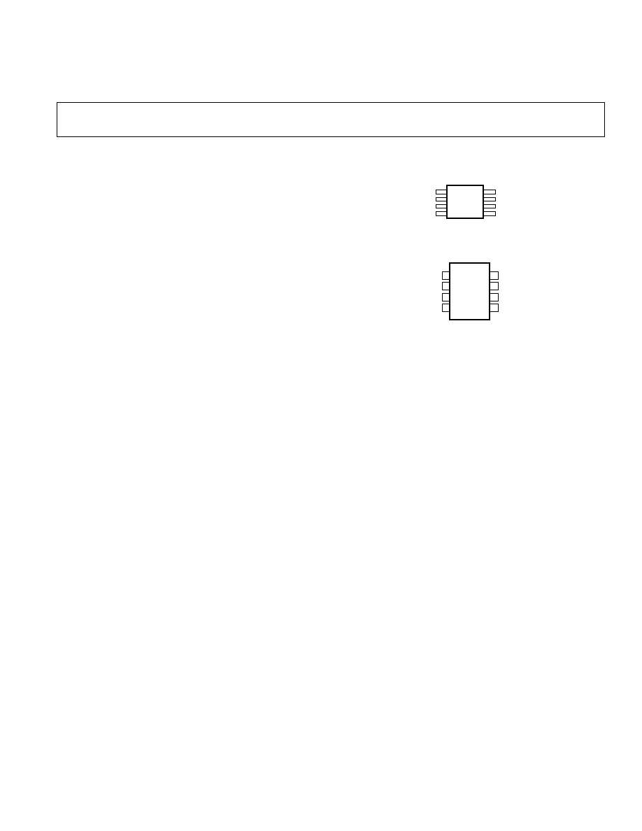
FUNCTIONAL BLOCK DIAGRAMS
8-Lead MSOP
(RM Suffix)
IN
IN
V
V+
OUT
NC
NC
1
4
5
8
OP777
NC
NC = NO CONNECT
8-Lead SOIC
(R Suffix)
1
2
3
4
8
7
6
5
OP777
IN
V
+IN
V+
OUT
NC
NC
NC
NC = NO CONNECT
FEATURES
Low Offset Voltage: 100 V Max
Low Input Bias Current: 10 nA Max
Single-Supply Operation: 2.7 V to 30 V
Dual-Supply Operation: 1.35 V to 15 V
Low Supply Current: 270 A/Amp
Unity Gain Stable
No Phase Reversal
APPLICATIONS
Precision Current Measurement
Line or Battery-Powered Instrumentation
Remote Sensors
Precision Filters
GENERAL DESCRIPTION
The OP777 is a precision single supply amplifier featuring
micropower operation and rail-to-rail output ranges. This ampli-
fier provides improved performance over the industry-standard
OP07 with
±15 V supplies and offers the further advantage of
true single supply operation down to 2.7 V, and smaller package
footprint than any other high-voltage precision bipolar amplifier.
Outputs are stable with capacitive loads of over 1000 pF. Supply
current is less than 300
µA per amplifier at 5 V. 500 series resis-
tors protect the inputs, allowing input signal levels to exceed either
power supply rail by up to 3 V without causing phase reversal of the
output signal or causing damage to the amplifier. The proprietary
fabrication process yields a very low-voltage noise corner frequency
under 10 Hz, greatly improving the low-frequency noise perfor-
mance of the OP07 and similar amplifiers. The specially fabricated
input PNP transistors operate with very low input bias currents while
allowing operation with large differential voltages, eliminating a
common limitation of many precision amplifiers and enabling
application of the OP777 in precision comparator and rectifier
circuits. This large differential voltage capability also further reduces
the need for external protection devices such as clamping diodes.
Applications for these amplifiers include both line powered and
portable instrumentation, remote sensor signal conditioning, and
precision filters.
The OP777 is specified over the extended industrial (≠40
∞C to
+85
∞C) temperature range and is available in 8-lead MSOP and
8-lead SOIC packages. The OP777 uses a standard operational
amplifier pinout, allowing for easy drop-in replacement of lower
performance amplifiers in most circuits. Surface mount devices
in MSOP packages are available in tape and reel only.

≠2≠
REV. 0
OP777≠SPECIFICATIONS
ELECTRICAL CHARACTERISTICS
Parameter
Symbol
Conditions
Min
Typ
Max
Unit
INPUT CHARACTERISTICS
Offset Voltage
V
OS
100
µV
≠40
∞C T
A
+85∞C
200
µV
Input Bias Current
I
B
≠40
∞C T
A
+85∞C
11
nA
Input Offset Current
I
OS
≠40
∞C T
A
+85∞C
2
nA
Input Voltage Range
0
4
V
Common-Mode Rejection Ratio
CMRR
V
CM
= 0 V to 4 V
104
110
dB
Large Signal Voltage Gain
A
VO
R
L
= 10 k
, V
O
= 0.5 V to 4.5 V
300
500
V/mV
Offset Voltage Drift
V
OS
/
T
≠40
∞C T
A
+85∞C
0.3
1.3
µV/∞C
OUTPUT CHARACTERISTICS
Output Voltage High
V
OH
I
L
= 1 mA, ≠40
∞C T
A
+85∞C
4.88
V
Output Voltage Low
V
OL
I
L
= 1 mA, ≠40
∞C T
A
+85∞C
140
mV
Short Circuit Limit
I
OUT
V
DROPOUT
< 1 V
±10
mA
POWER SUPPLY
Power Supply Rejection Ratio
PSRR
V
S
= 3 V to 30 V
120
130
dB
Supply Current/Amplifier
I
SY
V
O
= 0 V
270
µA
≠40
∞C T
A
+85∞C
270
320
µA
DYNAMIC PERFORMANCE
Slew Rate
SR
R
L
= 2 k
0.2
V/
µs
Gain Bandwidth Product
GBP
0.7
MHz
NOISE PERFORMANCE
Voltage Noise
e
n
p-p
0.1 Hz to 10 Hz
0.4
µVp-p
Voltage Noise Density
e
n
f = 1 kHz
15
nV/
Hz
Current Noise Density
i
n
f = 1 kHz
0.13
pA/
Hz
Specifications subject to change without notice.
(V
S
= 5.0 V, V
CM
= 2.5 V, T
A
= 25 C unless otherwise noted)

≠3≠
REV. 0
OP777
ELECTRICAL CHARACTERISTICS
Parameter
Symbol
Conditions
Min
Typ
Max
Unit
INPUT CHARACTERISTICS
Offset Voltage
V
OS
100
µV
≠40
∞C T
A
+85∞C
200
µV
Input Bias Current
I
B
≠40
∞C T
A
+85∞C
10
nA
Input Offset Current
I
OS
≠40
∞C T
A
+85∞C
2
nA
Input Voltage Range
≠15
+14
V
Common-Mode Rejection Ratio
CMRR
V
CM
= ≠15 V to +14 V
110
120
dB
Large Signal Voltage Gain
A
VO
R
L
= 10 k
, V
O
= ≠14.5 V to +14.5 V
1,000
2,500
V/mV
Offset Voltage Drift
V
OS
/
T
≠40
∞C T
A
+85∞C
0.3
1.3
µV/∞C
OUTPUT CHARACTERISTICS
Output Voltage High
V
OH
I
L
= 1 mA, ≠40
∞C T
A
+85∞C
14.9
V
Output Voltage Low
V
OL
I
L
= 1 mA, ≠40
∞C T
A
+85∞C
≠14.9
V
Short Circuit Limit
I
OUT
±30
mA
POWER SUPPLY
Power Supply Rejection Ratio
PSRR
V
S
=
±1.5 V to ±15 V
120
130
dB
Supply Current/Amplifier
I
SY
V
O
= 0 V
350
µA
≠40
∞C T
A
+85∞C
350
400
µA
DYNAMIC PERFORMANCE
Slew Rate
SR
R
L
= 2 k
0.2
V/
µs
Gain Bandwidth Product
GBP
0.7
MHz
NOISE PERFORMANCE
Voltage Noise
e
n
p-p
0.1 Hz to 10 Hz
0.4
µVp-p
Voltage Noise Density
e
n
f = 1 kHz
15
nV/
Hz
Current Noise Density
i
n
f = 1 kHz
0.13
pA/
Hz
Specifications subject to change without notice.
(V
S
= 15.0 V, V
CM
= 0 V, T
A
= 25 C unless otherwise noted)
OP777
≠4≠
REV. 0
ABSOLUTE MAXIMUM RATINGS
*
Supply Voltage . . . . . . . . . . . . . . . . . . . . . . . . . . . . . . . . . 36 V
Input Voltage . . . . . . . . . . . . . . . . . . . . . V
S≠
≠ 3 V to V
S+
+ 3 V
Differential Input Voltage . . . . . . . . . . . . . .
± Supply Voltage
Output Short-Circuit Duration to GND . . . . . . . . . Indefinite
Storage Temperature Range
R, RM Packages . . . . . . . . . . . . . . . . . . . . ≠65
∞C to +150∞C
Operating Temperature Range
OP777 . . . . . . . . . . . . . . . . . . . . . . . . . . . . ≠40
∞C to +85∞C
Junction Temperature Range
R, RM Packages . . . . . . . . . . . . . . . . . . . . ≠65
∞C to +150∞C
Lead Temperature Range (Soldering, 60 sec) . . . . . . . . 300
∞C
ESD (HBM) . . . . . . . . . . . . . . . . . . . . . . . . . . . . . . . . . . 2 kV
*Stresses above those listed under Absolute Maximum Ratings may cause perma-
nent damage to the device. This is a stress rating only; functional operation of the
device at these or any other conditions above those listed in the operational sections
of this specification is not implied. Exposure to absolute maximum rating condi-
tions for extended periods may affect device reliability.
Package Type
JA
1
JC
Unit
8-Lead MSOP (RM)
190
44
∞C/W
8-Lead SOIC (R)
158
43
∞C/W
NOTE
1
JA
is specified for worst-case conditions, i.e.,
JA
is specified for device soldered
in circuit board for surface-mount packages.
CAUTION
ESD (electrostatic discharge) sensitive device. Electrostatic charges as high as 4000 V readily
accumulate on the human body and test equipment and can discharge without detection. Although
the OP777 features proprietary ESD protection circuitry, permanent damage may occur on devices
subjected to high-energy electrostatic discharges. Therefore, proper ESD precautions are recom-
mended to avoid performance degradation or loss of functionality.
WARNING!
ESD SENSITIVE DEVICE
ORDERING GUIDE
Temperature
Package
Package
Branding
Model
Range
Description
Option
Information
OP777ARM
≠40
∞C to +85∞C
8-Lead MSOP
RM-8
A1A
OP777AR
≠40
∞C to +85∞C
8-Lead SOIC
SO-8

OP777
≠5≠
REV. 0
OFFSET VOLTAGE ≠ V
220
60
0
100
80 60
40 20
0
20
40
60 80 100
200
80
40
20
160
120
140
100
180
V
SY
= 15V
V
CM
= 0V
T
A
= 25 C
NUMBER OF AMPLIFIERS
Figure 1. Input Offset Voltage
Distribution
INPUT BIAS CURRENT ≠ nA
NUMBER OF AMPLIFIERS
30
15
0
3
8
4
5
6
7
25
20
10
5
V
SY
= 15V
V
CM
= 0V
T
A
= 25 C
Figure 4. Input Bias Current
Distribution
TEMPERATURE ≠ C
INPUT BIAS CURRENT
≠
nA
10
5
30
60
40
140
20 0
20
40
60
80 100 120
5
0
15
25
10
20
V
SY
= 15V
Figure 7. Input Bias Current vs.
Temperature
OFFSET VOLTAGE ≠ V
220
60
0
100
80 60
40 20
0
20
40
60 80 100
200
80
40
20
160
120
140
100
180
V
SY
= 5V
V
CM
= 2.5V
T
A
= 25 C
NUMBER OF AMPLIFIERS
Figure 2. Input Offset Voltage
Distribution
LOAD CURRENT ≠ mA
OUTPUT VOLTAGE
≠
mV
10k
100
0
0.001
0.01
100
0.1
1
10
1.0
V
S
= 5V
T
A
= 25 C
0.1
10
1k
SINK
SOURCE
Figure 5. Output Voltage to Supply
Rail vs. Load Current
TEMPERATURE ≠ C
SUPPLY CURRENT
≠
A
500
500
60
40
140
20 0
20
40
60
80 100 120
200
100
200
400
100
300
I
SY+
(V
SY
= 15V)
0
400
I
SY+
(V
SY
= 5V)
I
SY
(V
SY
= 5V)
I
SY
(V
SY
= 15V)
Figure 8. Supply Current vs.
Temperature
INPUT OFFSET DRIFT ≠ V/ C
NUMBER OF AMPLIFIERS
30
15
0
0
1.2
0.2
0.4
0.6
0.8
1.0
25
20
10
5
V
SY
= 15V
V
CM
= 0V
T
A
= 40 C TO +85 C
Figure 3. Input Offset Voltage Drift
Distribution
LOAD CURRENT ≠ mA
OUTPUT VOLTAGE
≠
mV
10k
100
0
0.001
0.01
100
0.1
1
10
1.0
SOURCE
V
S
= 15V
T
A
= 25 C
0.1
10
1k
SINK
Figure 6. Output Voltage to Supply
Rail vs. Load Current
SUPPLY VOLTAGE ≠ V
SUPPLY CURRENT
≠
A
350
0
0
5
35
10
15
20
25
30
300
200
150
100
50
250
T
A
= 25 C
Figure 9. Supply Current vs.
Supply Voltage
Typical Performance Characteristics≠