 | ÐлекÑÑоннÑй компоненÑ: REF195B | СкаÑаÑÑ:  PDF PDF  ZIP ZIP |
REF19x Series
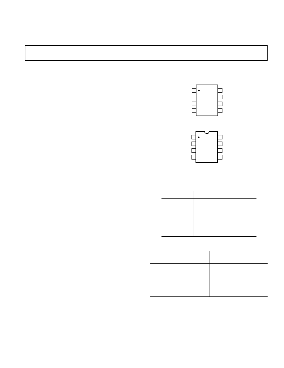
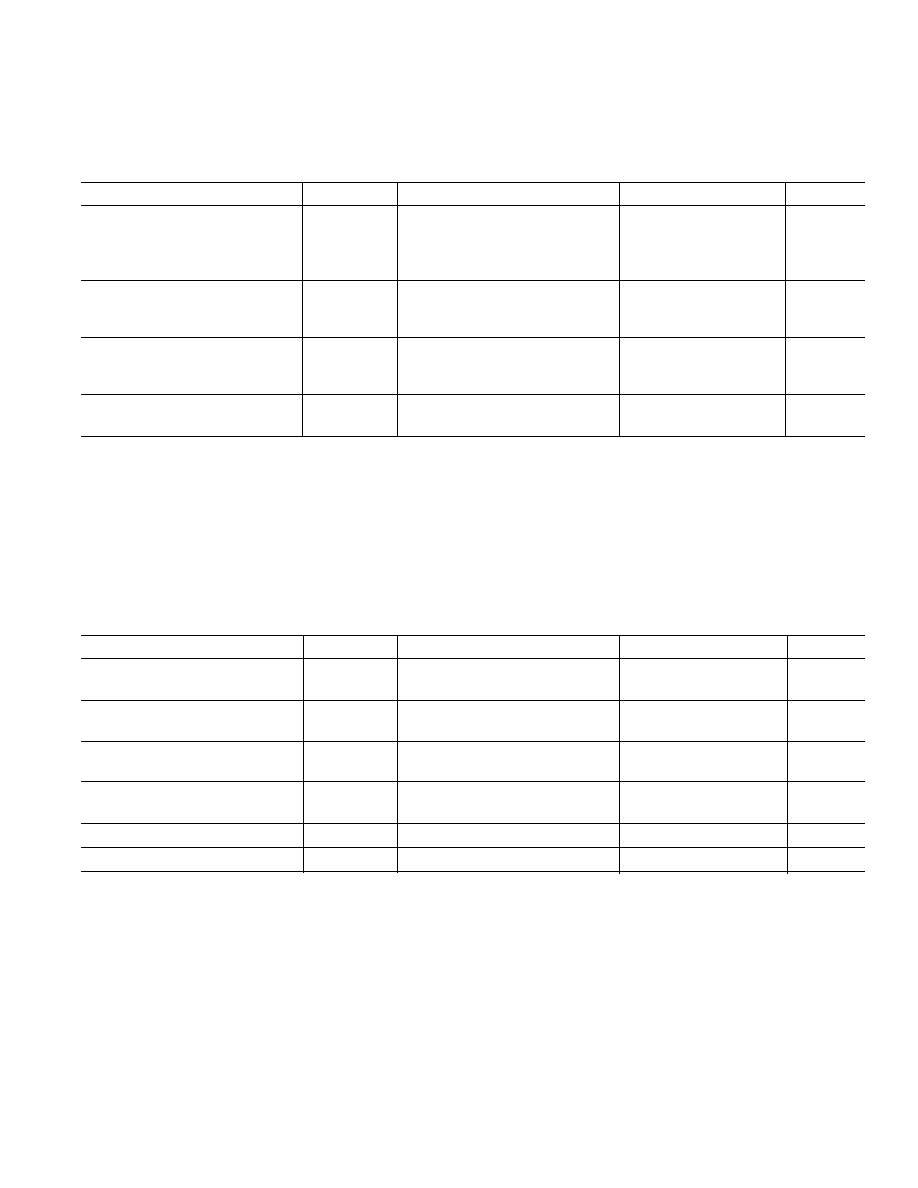
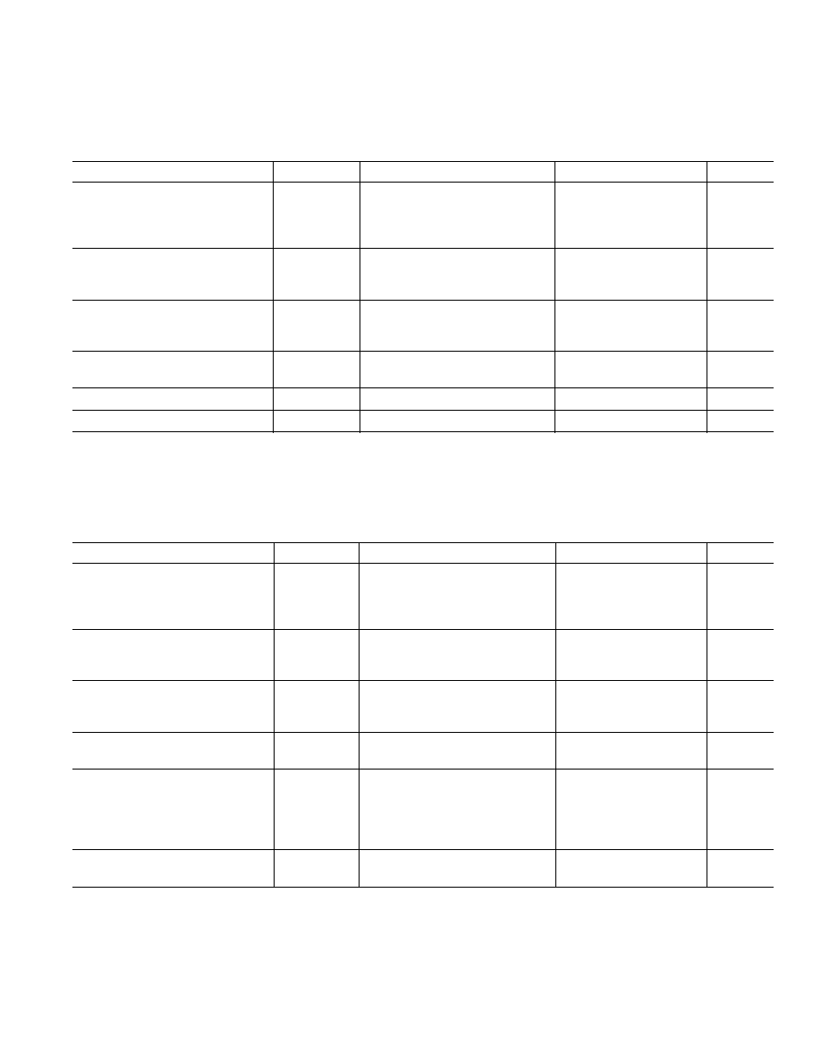
Table I
Part Number
Nominal Output Voltage (V)
REF191
2.048
REF192
2.50
REF193
3.00
REF194
4.50
REF195
5.00
REF196
3.30
REF198
4.096
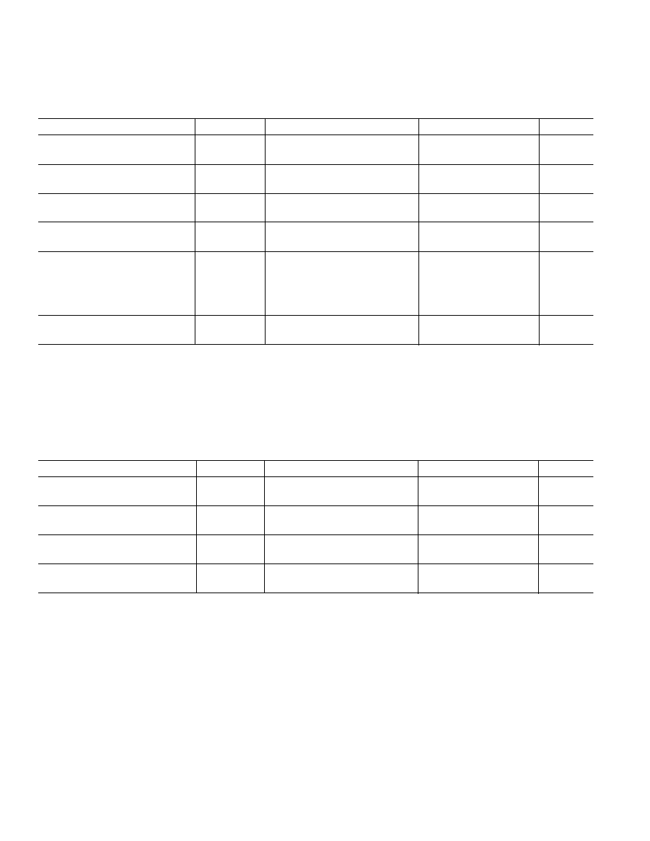
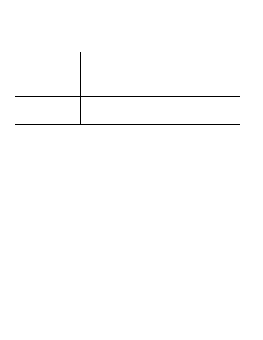
ORDERING GUIDE
Temperature
Package
Package
Model
Range
Description
Option
1
REF19xGP
40
°
C to +85
°
C
8-Lead Plastic DIP
2
N-8
REF19xES
3
40
°
C to +85
°
C
8-Lead SOIC
SO-8
REF19xFS
3
40
°
C to +85
°
C
8-Lead SOIC
SO-8
REF19xGS
40
°
C to +85
°
C
8-Lead SOIC
SO-8
REF19xGRU 40
°
C to +85
°
C
8-Lead TSSOP
RU-8
REF19xGBC
+25
°
C
DICE
NOTES
1
N = Plastic DIP,
SO = Small Outline, RU = Thin Shrink Small Outline.
2
8-Lead plastic DIP only available in "G" grade.
3
REF193 and REF196 are available in "G" grade only.
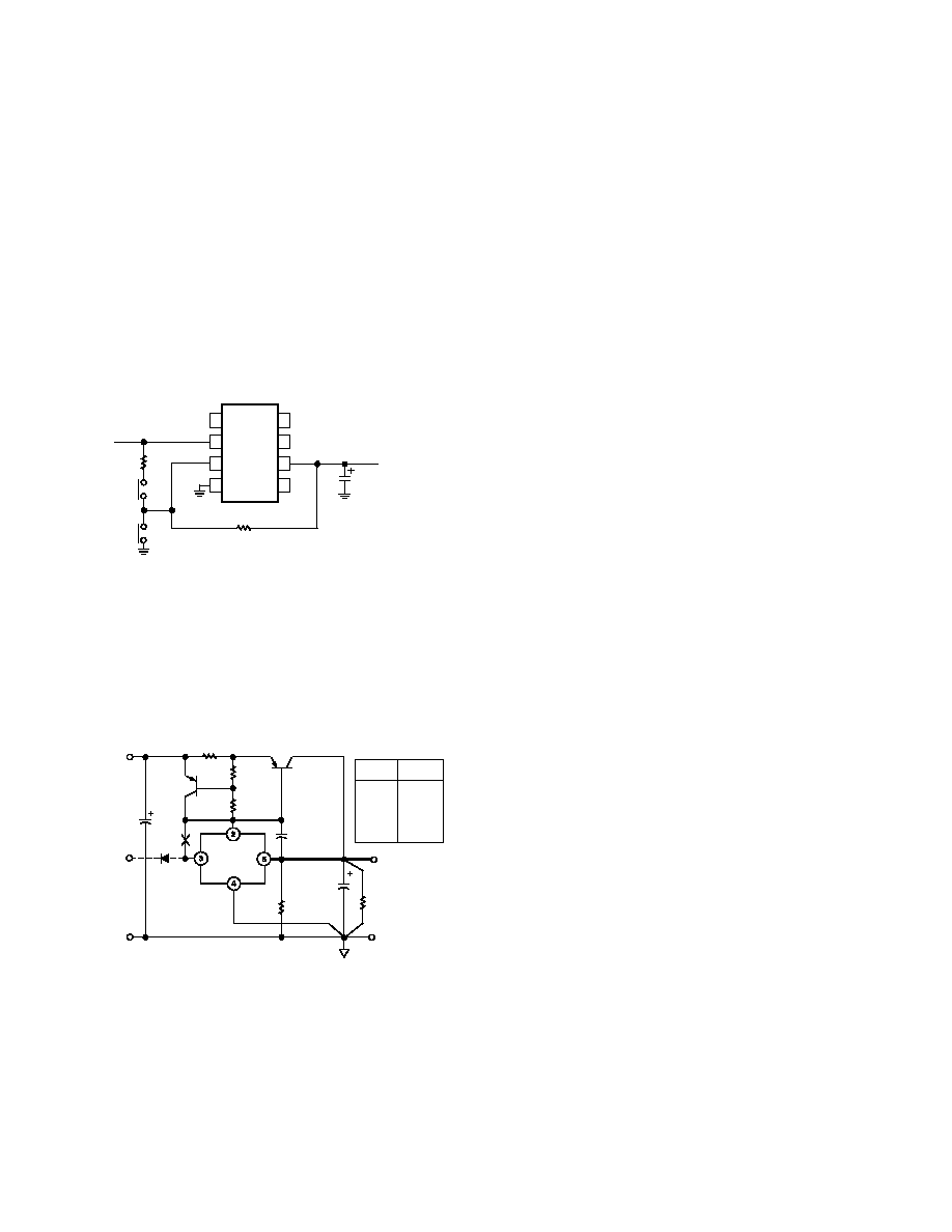
PIN CONFIGURATIONS
a
Precision Micropower, Low Dropout,
Voltage References
REF19x Series
8-Lead Narrow-Body SO and TSSOP
(S Suffix and RU Suffix)
TP
V
S
SLEEP
GND
NC
NC
OUTPUT
TP
1
2
3
4
8
7
6
5
REF19x
SERIES
TOP VIEW
(Not to Scale)
REV. D
Information furnished by Analog Devices is believed to be accurate and
reliable. However, no responsibility is assumed by Analog Devices for its
use, nor for any infringements of patents or other rights of third parties
which may result from its use. No license is granted by implication or
otherwise under any patent or patent rights of Analog Devices.
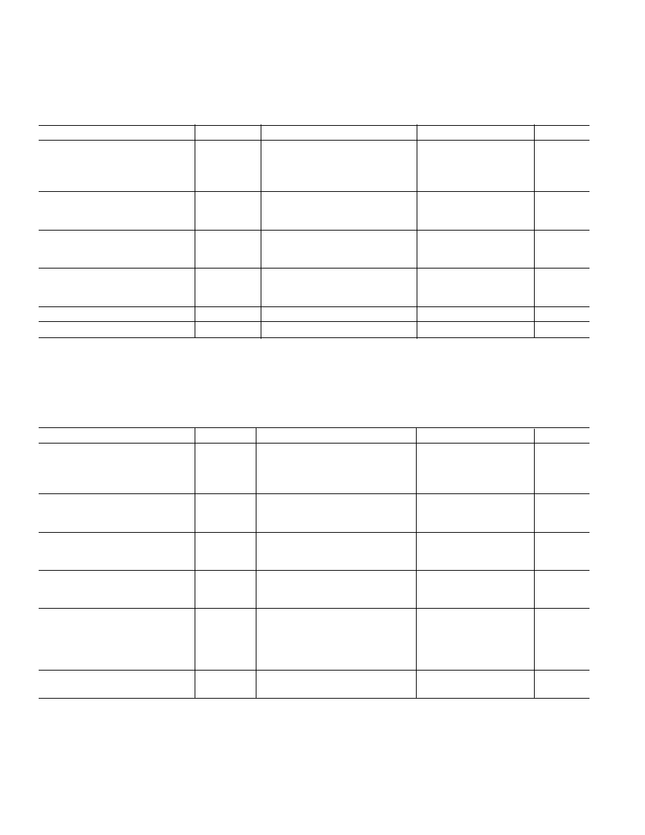
8-Lead Epoxy DIP (P Suffix)
TP
V
S
SLEEP
GND
NC = NO CONNECT
TP PINS ARE FACTORY TEST POINTS
NO USER CONNECTION
NC
NC
OUTPUT
TP
1
2
3
4
8
7
6
5
REF19x
SERIES
TOP VIEW
(Not to Scale)
FEATURES
Initial Accuracy: 2 mV max
Temperature Coefficient: 5 ppm/
°
C max
Low Supply Current: 45 A max
Sleep Mode: 15 A max
Low Dropout Voltage
Load Regulation: 4 ppm/mA
Line Regulation: 4 ppm/V
High Output Current: 30 mA
Short Circuit Protection
APPLICATIONS
Portable Instrumentation
A-to-D and D-to-A Converters
Smart Sensors
Solar Powered Applications
Loop Current Powered Instrumentations
GENERAL DESCRIPTION
REF19x series precision bandgap voltage references use a pat-
ented temperature drift curvature correction circuit and laser
trimming of highly stable thin film resistors to achieve a very low
temperature coefficient and a high initial accuracy.
The REF19x series are micropower, Low Dropout Voltage
(LDV) devices providing a stable output voltage from supplies
as low as 100 mV above the output voltage and consuming less
than 45
µ
A of supply current. In sleep mode, which is enabled
by applying a low TTL or CMOS level to the sleep pin, the
output is turned off and supply current is further reduced to less
than 15
µ
A.
The REF19x series references are specified over the extended
industrial temperature range (40
°
C to +85
°
C) with typical
performance specifications over 40
°
C to +125
°
C for applica-
tions such as automotive.
All electrical grades are available in 8-Lead SOIC; the PDIP and
TSSOP are only available in the lowest electrical grade. Prod-
ucts are also available in die form.
Test Pins (TP)
The test pins, Pin 1 and Pin 5, are reserved for in-package
zener-zap. To achieve the highest level of accuracy at the out-
put, the zener-zapping technique is used to trim the output
voltage. Since each unit may require a different amount of ad-
justment, the resistance value at the test pins will vary widely
from pin-to-pin as well as from part-to-part. The user should
not make any physical nor electrical connections to Pin 1 and
Pin 5.
One Technology Way, P.O. Box 9106, Norwood, MA 02062-9106, U.S.A.
Tel: 781/329-4700
World Wide Web Site: http://www.analog.com
Fax: 781/326-8703
© Analog Devices, Inc., 1999
REF19x Series
2
REV. D
REF191SPECIFICATIONS
ELECTRICAL CHARACTERISTICS
Parameter
Symbol
Condition
Min
Typ
Max
Units
INITIAL ACCURACY
1
"E" Grade
V
O
I
OUT
= 0 mA
2.046
2.048
2.050
V
"F" Grade
2.043
2.053
V
"G" Grade
2.038
2.058
V
LINE REGULATION
2
"E" Grade
V
O
/
V
IN
3.0 V
V
S
15 V, I
OUT
= 0 mA
2
4
ppm/V
"F & G" Grades
4
8
ppm/V
LOAD REGULATION
2
"E" Grade
V
O
/
V
LOAD
V
S
= 5.0 V, 0
I
OUT
30 mA
4
10
ppm/mA
"F & G" Grades
6
15
ppm/mA
DROPOUT VOLTAGE
V
S
V
O
V
S
= 3.15 V, I
LOAD
= 2 mA
0.95
V
V
S
= 3.3 V, I
LOAD
= 10 mA
1.25
V
V
S
= 3.6 V, I
LOAD
= 30 mA
1.55
V
LONG-TERM STABILITY
3
V
O
1000 Hours @ +125
°
C
1.2
mV
NOISE VOLTAGE
e
N
0.1 Hz to 10 Hz
20
µ
V p-p
NOTES
1
Initial accuracy includes temperature hysteresis effect.
2
Line and load regulation specifications include the effect of self-heating.
3
Long-term drift is guaranteed by 1000 hours life test performed on three independent wafer lots at +125
°
C, with an LTPD of 1.3.
Specifications subject to change without notice.
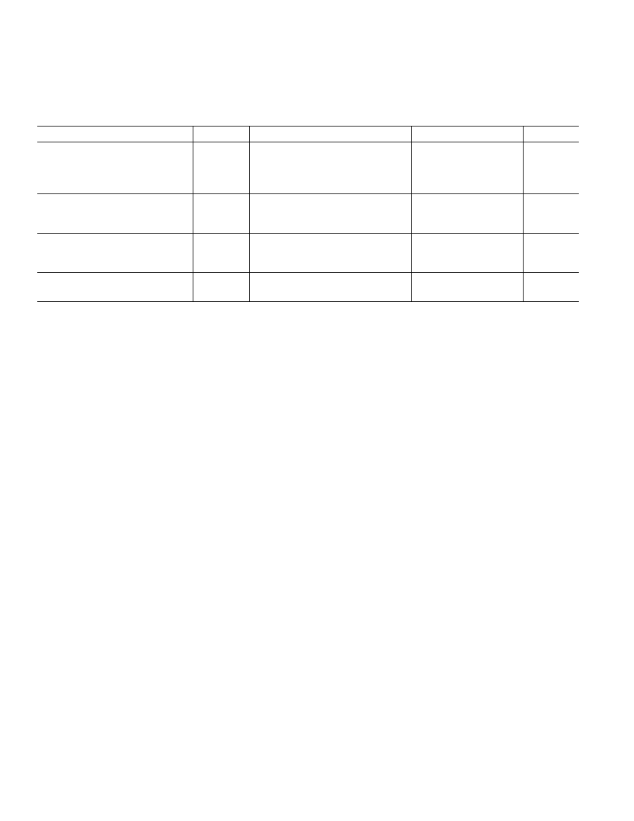
ELECTRICAL CHARACTERISTICS
Parameter
Symbol
Condition
Min
Typ
Max
Units
TEMPERATURE COEFFICIENT
1, 2
"E" Grade
TCV
O
/
°
C
I
OUT
= 0 mA
2
5
ppm/
°
C
"F" Grade
5
10
ppm/
°
C
"G" Grade
3
10
25
ppm/
°
C
LINE REGULATION
4
"E" Grade
V
O
/
V
IN
3.0 V
V
S
15 V, I
OUT
= 0 mA
5
10
ppm/V
"F & G" Grades
10
20
ppm/V
LOAD REGULATION
4
"E" Grade
V
O
/
V
LOAD
V
S
= 5.0 V, 0
I
OUT
25 mA
5
15
ppm/mA
"F & G" Grades
10
20
ppm/mA
DROPOUT VOLTAGE
V
S
V
O
V
S
= 3.15 V, I
LOAD
= 2 mA
0.95
V
V
S
= 3.3 V, I
LOAD
= 10 mA
1.25
V
V
S
= 3.6 V, I
LOAD
= 25 mA
1.55
V
SLEEP PIN
Logic High Input Voltage
V
H
2.4
V
Logic High Input Current
I
H
8
µ
A
Logic Low Input Voltage
V
L
0.8
V
Logic Low Input Current
I
L
8
µ
A
SUPPLY CURRENT
No Load
45
µ
A
Sleep Mode
No Load
15
µ
A
NOTES
1
For proper operation, a 1
µ
F capacitor is required between the output pin and the GND pin of the device.
2
TCV
O
is defined as the ratio of output change with temperature variation to the specified temperature range expressed in ppm/
°
C.
TCV
O
= (V maxV min)/V
O
(T
MAX
T
MIN
).
3
Guaranteed by characterization.
4
Line and load regulation specifications include the effect of self-heating.
Specifications subject to change without notice.
(@ V
S
= 3.3 V, T
A
= +25 C unless otherwise noted)
(@ V
S
= 3.3 V, 40 C
T
A
+85 C unless otherwise noted)
REF191SPECIFICATIONS
ELECTRICAL CHARACTERISTICS
Parameter
Symbol
Condition
Min
Typ
Max
Units
TEMPERATURE COEFFICIENT
1, 2
"E" Grade
TCV
O
/
°
C
I
OUT
= 0 mA
2
ppm/
°
C
"F" Grade
5
ppm/
°
C
"G" Grade
3
10
ppm/
°
C
LINE REGULATION
4
"E" Grade
V
O
/
V
IN
3.0 V
V
S
15 V, I
OUT
= 0 mA
10
ppm/V
"F & G" Grades
20
ppm/V
LOAD REGULATION
4
"E" Grade
V
O
/
V
LOAD
V
S
= 5.0 V, 0
I
OUT
20 mA
10
ppm/mA
"F & G" Grades
20
ppm/mA
DROPOUT VOLTAGE
V
S
V
O
V
S
= 3.3 V, I
LOAD
= 10 mA
1.25
V
V
S
= 3.6 V, I
LOAD
= 20 mA
1.55
V
NOTES
1
For proper operation, a 1
µ
F capacitor is required between the output pin and the GND pin of the device.
2
TCV
O
is defined as the ratio of output change with temperature variation to the specified temperature range expressed in ppm/
°
C.
TCV
O
= (V maxV min)/V
O
(T
MAX
T
MIN
).
3
Guaranteed by characterization.
4
Line and load regulation specifications include the effect of self-heating.
Specifications subject to change without notice.
REF19x Series
REV. D
3
(@ V
S
= 3.3 V, 40 C
T
A
+125 C unless otherwise noted)
REF19x Series
4
REV. D
REF192SPECIFICATIONS
ELECTRICAL CHARACTERISTICS
Parameter
Symbol
Condition
Min
Typ
Max
Units
INITIAL ACCURACY
1
"E" Grade
V
O
I
OUT
= 0 mA
2.498
2.500
2.502
V
"F" Grade
2.495
2.505
V
"G" Grade
2.490
2.510
V
LINE REGULATION
2
"E" Grade
V
O
/
V
IN
3.0 V
V
S
15 V, I
OUT
= 0 mA
2
4
ppm/V
"F & G" Grades
4
8
ppm/V
LOAD REGULATION
2
"E" Grade
V
O
/
V
LOAD
V
S
= 5.0 V, 0
I
OUT
30 mA
4
10
ppm/mA
"F & G" Grades
6
15
ppm/mA
DROPOUT VOLTAGE
V
S
V
O
V
S
= 3.5 V, I
LOAD
= 10 mA
1.00
V
V
S
= 3.9 V, I
LOAD
= 30 mA
1.40
V
LONG-TERM STABILITY
3
V
O
1000 Hours @ +125
°
C
1.2
mV
NOISE VOLTAGE
e
N
0.1 Hz to 10 Hz
25
µ
V p-p
NOTES
1
Initial accuracy includes temperature hysteresis effect.
2
Line and load regulation specifications include the effect of self-heating.
3
Long-term drift is guaranteed by 1000 hours life test performed on three independent wafer lots at +125
°
C, with an LTPD of 1.3.
Specifications subject to change without notice.
ELECTRICAL CHARACTERISTICS
Parameter
Symbol
Condition
Min
Typ
Max
Units
TEMPERATURE COEFFICIENT
1, 2
"E" Grade
TCV
O
/
°
C
I
OUT
= 0 mA
2
5
ppm/
°
C
"F" Grade
5
10
ppm/
°
C
"G" Grade
3
10
25
ppm/
°
C
LINE REGULATION
4
"E" Grade
V
O
/
V
IN
3.0 V
V
S
15 V, I
OUT
= 0 mA
5
10
ppm/V
"F & G" Grades
10
20
ppm/V
LOAD REGULATION
4
"E" Grade
V
O
/
V
LOAD
V
S
= 5.0 V, 0
I
OUT
25 mA
5
15
ppm/mA
"F & G" Grades
10
20
ppm/mA
DROPOUT VOLTAGE
V
S
V
O
V
S
= 3.5 V, I
LOAD
= 10 mA
1.00
V
V
S
= 4.0 V, I
LOAD
= 25 mA
1.50
V
SLEEP PIN
Logic High Input Voltage
V
H
2.4
V
Logic High Input Current
I
H
8
µ
A
Logic Low Input Voltage
V
L
0.8
V
Logic Low Input Current
I
L
8
µ
A
SUPPLY CURRENT
No Load
45
µ
A
Sleep Mode
No Load
15
µ
A
NOTES
1
For proper operation, a 1
µ
F capacitor is required between the output pin and the GND pin of the device.
2
TCV
O
is defined as the ratio of output change with temperature variation to the specified temperature range expressed in ppm/
°
C.
TCV
O
= (V maxV min)/V
O
(T
MAX
T
MIN
).
3
Guaranteed by characterization.
4
Line and load regulation specifications include the effect of self-heating.
Specifications subject to change without notice.
(@ V
S
= 3.3 V, T
A
= +25 C unless otherwise noted)
(@ V
S
= 3.3 V, T
A
= 40 C
T
A
+85 C unless otherwise noted)
REF192SPECIFICATIONS
ELECTRICAL CHARACTERISTICS
Parameter
Symbol
Condition
Min
Typ
Max
Units
TEMPERATURE COEFFICIENT
1, 2
"E" Grade
TCV
O
/
°
C
I
OUT
= 0 mA
2
ppm/
°
C
"F" Grade
5
ppm/
°
C
"G" Grade
3
10
ppm/
°
C
LINE REGULATION
4
"E" Grade
V
O
/
V
IN
3.0 V
V
S
15 V, I
OUT
= 0 mA
10
ppm/V
"F & G" Grades
20
ppm/V
LOAD REGULATION
4
"E" Grade
V
O
/
V
LOAD
V
S
= 5.0 V, 0
I
OUT
20 mA
10
ppm/mA
"F & G" Grades
20
ppm/mA
DROPOUT VOLTAGE
V
S
V
O
V
S
= 3.5 V, I
LOAD
= 10 mA
1.00
V
V
S
= 4.0 V, I
LOAD
= 20 mA
1.50
V
NOTES
1
For proper operation, a 1
µ
F capacitor is required between the output pin and the GND pin of the device.
2
TCV
O
is defined as the ratio of output change with temperature variation to the specified temperature range expressed in ppm/
°
C.
TCV
O
= (V maxV min)/V
O
(T
MAX
T
MIN
).
3
Guaranteed by characterization.
4
Line and load regulation specifications include the effect of self-heating.
Specifications subject to change without notice.
REF19x Series
5
REV. D
(@ V
S
= 3.3 V, 40 C
T
A
+125 C unless otherwise noted)
REF193SPECIFICATIONS
ELECTRICAL CHARACTERISTICS
Parameter
Symbol
Condition
Min
Typ
Max
Units
INITIAL ACCURACY
1
"G" Grade
V
O
I
OUT
= 0 mA
2.990
3.0
3.010
V
LINE REGULATION
2
"G" Grades
V
O
/
V
IN
3.3 V,
V
S
15 V, I
OUT
= 0 mA
4
8
ppm/V
LOAD REGULATION
2
"G" Grade
V
O
/
V
LOAD
V
S
= 5.0 V, 0
I
OUT
30 mA
6
15
ppm/mA
DROPOUT VOLTAGE
V
S
V
O
V
S
= 3.8 V, I
LOAD
= 10 mA
0.80
V
V
S
= 4.0 V, I
LOAD
= 30 mA
1.00
V
LONG-TERM STABILITY
3
V
O
1000 Hours @ +125
°
C
1.2
mV
NOISE VOLTAGE
e
N
0.1 Hz to 10 Hz
30
µ
V p-p
NOTES
1
Initial accuracy includes temperature hysteresis effect.
2
Line and load regulation specifications include the effect of self-heating.
3
Long-term drift is guaranteed by 1000 hours life test performed on three independent wafer lots at +125
°
C, with an LTPD of 1.3.
Specifications subject to change without notice.
(@ V
S
= 3.3 V, T
A
= +25 C unless otherwise noted)
REF19x Series
6
REV. D
REF193SPECIFICATIONS
ELECTRICAL CHARACTERISTICS
Parameter
Symbol
Condition
Min
Typ
Max
Units
TEMPERATURE COEFFICIENT
1, 2
"G" Grade
3
TCV
O
/
°
C
I
OUT
= 0 mA
10
25
ppm/
°
C
LINE REGULATION
4
"G" Grade
V
O
/
V
IN
3.3 V
V
S
15 V, I
OUT
= 0 mA
10
20
ppm/V
LOAD REGULATION
4
"G" Grade
V
O
/
V
LOAD
V
S
= 5.0 V, 0
I
OUT
25 mA
10
20
ppm/mA
DROPOUT VOLTAGE
V
S
V
O
V
S
= 3.8 V, I
LOAD
= 10 mA
0.80
V
V
S
= 4.1 V, I
LOAD
= 30 mA
1.10
V
SLEEP PIN
Logic High Input Voltage
V
H
2.4
V
Logic High Input Current
I
H
8
µ
A
Logic Low Input Voltage
V
L
0.8
V
Logic Low Input Current
I
L
8
µ
A
SUPPLY CURRENT
No Load
45
µ
A
Sleep Mode
No Load
15
µ
A
NOTES
1
For proper operation, a 1
µ
F capacitor is required between the output pin and the GND pin of the device.
2
TCV
O
is defined as the ratio of output change with temperature variation to the specified temperature range expressed in ppm/
°
C.
TCV
O
= (V maxV min)/V
O
(T
MAX
T
MIN
).
3
Guaranteed by characterization.
4
Line and load regulation specifications include the effect of self-heating.
Specifications subject to change without notice.
ELECTRICAL CHARACTERISTICS
Parameter
Symbol
Condition
Min
Typ
Max
Units
TEMPERATURE COEFFICIENT
1, 2
"G" Grade
3
TCV
O
/
°
C
I
OUT
= 0 mA
10
ppm/
°
C
LINE REGULATION
4
"G" Grade
V
O
/
V
IN
3.3 V
V
S
15 V, I
OUT
= 0 mA
20
ppm/V
LOAD REGULATION
4
"G" Grade
V
O
/
V
LOAD
V
S
= 5.0 V, 0
I
OUT
20 mA
10
ppm/mA
DROPOUT VOLTAGE
V
S
V
O
V
S
= 3.8 V, I
LOAD
= 10 mA
0.80
V
V
S
= 4.1 V, I
LOAD
= 20 mA
1.10
V
NOTES
1
For proper operation, a 1
µ
F capacitor is required between the output pin and the GND pin of the device.
2
TCV
O
is defined as the ratio of output change with temperature variation to the specified temperature range expressed in ppm/
°
C.
TCV
O
= (V maxV min)/V
O
(T
MAX
T
MIN
).
3
Guaranteed by characterization.
4
Line and load regulation specifications include the effect of self-heating.
Specifications subject to change without notice.
(@ V
S
= 3.3 V, 40 C
T
A
+125 C unless otherwise noted)
(@ V
S
= 3.3 V, T
A
= 40 C
T
A
+85 C unless otherwise noted)
REF194SPECIFICATIONS
ELECTRICAL CHARACTERISTICS
Parameter
Symbol
Condition
Min
Typ
Max
Units
INITIAL ACCURACY
1
"E" Grade
V
O
I
OUT
= 0 mA
4.498
4.5
4.502
V
"F" Grade
4.495
4.505
V
"G" Grade
4.490
4.510
V
LINE REGULATION
2
"E" Grade
V
O
/
V
IN
4.75 V
V
S
15 V, I
OUT
= 0 mA
2
4
ppm/V
"F & G" Grades
4
8
ppm/V
LOAD REGULATION
2
"E" Grade
V
O
/
V
LOAD
V
S
= 5.8 V, 0
I
OUT
30 mA
2
4
ppm/mA
"F & G" Grades
4
8
ppm/mA
DROPOUT VOLTAGE
V
S
V
O
V
S
= 5.00 V, I
LOAD
= 10 mA
0.50
V
V
S
= 5.8 V, I
LOAD
= 30 mA
1.30
V
LONG-TERM STABILITY
3
V
O
1000 Hours @ +125
°
C
2
mV
NOISE VOLTAGE
e
N
0.1 Hz to 10 Hz
45
µ
V p-p
NOTES
1
Initial accuracy includes temperature hysteresis effect.
2
Line and load regulation specifications include the effect of self-heating.
3
Long-term drift is guaranteed by 1000 hours life test performed on three independent wafer lots at +125
°
C, with an LTPD of 1.3.
Specifications subject to change without notice.
ELECTRICAL CHARACTERISTICS
Parameter
Symbol
Condition
Min
Typ
Max
Units
TEMPERATURE COEFFICIENT
1, 2
"E" Grade
TCV
O
/
°
C
I
OUT
= 0 mA
2
5
ppm/
°
C
"F" Grade
5
10
ppm/
°
C
"G" Grade
3
10
25
ppm/
°
C
LINE REGULATION
4
"E" Grade
V
O
/
V
IN
4.75 V
V
S
15 V, I
OUT
= 0 mA
5
10
ppm/V
"F & G" Grades
10
20
ppm/V
LOAD REGULATION
4
"E" Grade
V
O
/
V
LOAD
V
S
= 5.80 V, 0
I
OUT
25 mA
5
15
ppm/mA
"F & G" Grades
10
20
ppm/mA
DROPOUT VOLTAGE
V
S
V
O
V
S
= 5.00 V, I
LOAD
= 10 mA
0.5
V
V
S
= 5.80 V, I
LOAD
= 25 mA
1.30
V
SLEEP PIN
Logic High Input Voltage
V
H
2.4
V
Logic High Input Current
I
H
8
µ
A
Logic Low Input Voltage
V
L
0.8
V
Logic Low Input Current
I
L
8
µ
A
SUPPLY CURRENT
No Load
45
µ
A
Sleep Mode
No Load
15
µ
A
NOTES
1
For proper operation, a 1
µ
F capacitor is required between the output pin and the GND pin of the device.
2
TCV
O
is defined as the ratio of output change with temperature variation to the specified temperature range expressed in ppm/
°
C.
TCV
O
= (V maxV min)/V
O
(T
MAX
T
MIN
).
3
Guaranteed by characterization.
4
Line and load regulation specifications include the effect of self-heating.
Specifications subject to change without notice.
REF19x Series
7
REV. D
(@ V
S
= 5.0 V, T
A
= 40 C
T
A
+85 C unless otherwise noted)
(@ V
S
= 5.0 V, T
A
= +25 C unless otherwise noted)
REF19x Series
8
REV. D
REF194SPECIFICATIONS
ELECTRICAL CHARACTERISTICS
Parameter
Symbol
Condition
Min
Typ
Max
Units
TEMPERATURE COEFFICIENT
1, 2
"E" Grade
TCV
O
/
°
C
I
OUT
= 0 mA
2
ppm/
°
C
"F" Grade
5
ppm/
°
C
"G" Grade
3
10
ppm/
°
C
LINE REGULATION
4
"E" Grade
V
O
/
V
IN
4.75 V
V
S
15 V, I
OUT
= 0 mA
5
ppm/V
"F & G" Grades
10
ppm/V
LOAD REGULATION
4
"E" Grade
V
O
/
V
LOAD
V
S
= 5.80 V, 0
I
OUT
20 mA
5
ppm/mA
"F & G" Grades
10
ppm/mA
DROPOUT VOLTAGE
V
S
V
O
V
S
= 5.10 V, I
LOAD
= 10 mA
0.60
V
V
S
= 5.95 V, I
LOAD
= 20 mA
1.45
V
NOTES
1
For proper operation, a 1
µ
F capacitor is required between the output pin and the GND pin of the device.
2
TCV
O
is defined as the ratio of output change with temperature variation to the specified temperature range expressed in ppm/
°
C.
TCV
O
= (V maxV min)/V
O
(T
MAX
T
MIN
).
3
Guaranteed by characterization.
4
Line and load regulation specifications include the effect of self-heating.
Specifications subject to change without notice.
(@ V
S
= 5.0 V, 40 C
T
A
+125 C unless otherwise noted)
REF195SPECIFICATIONS
ELECTRICAL CHARACTERISTICS
Parameter
Symbol
Condition
Min
Typ
Max
Units
INITIAL ACCURACY
1
"E" Grade
V
O
I
OUT
= 0 mA
4.998
5.0
5.002
V
"F" Grade
4.995
5.005
V
"G" Grade
4.990
5.010
V
LINE REGULATION
2
"E" Grade
V
O
/
V
IN
5.10 V
V
S
15 V, I
OUT
= 0 mA
2
4
ppm/V
"F & G" Grades
4
8
ppm/V
LOAD REGULATION
2
"E" Grade
V
O
/
V
LOAD
V
S
= 6.30 V, 0
I
OUT
30 mA
2
4
ppm/mA
"F & G" Grades
4
8
ppm/mA
DROPOUT VOLTAGE
V
S
V
O
V
S
= 5.50 V, I
LOAD
= 10 mA
0.50
V
V
S
= 6.30 V, I
LOAD
= 30 mA
1.30
V
LONG-TERM STABILITY
3
V
O
1000 Hours @ +125
°
C
1.2
mV
NOISE VOLTAGE
e
N
0.1 Hz to 10 Hz
50
µ
V p-p
NOTES
1
Initial accuracy includes temperature hysteresis effect.
2
Line and load regulation specifications include the effect of self-heating.
3
Long-term drift is guaranteed by 1000 hours life test performed on three independent wafer lots at +125
°
C, with an LTPD of 1.3.
Specifications subject to change without notice.
ELECTRICAL CHARACTERISTICS
Parameter
Symbol
Condition
Min
Typ
Max
Units
TEMPERATURE COEFFICIENT
1, 2
"E" Grade
TCV
O
/
°
C
I
OUT
= 0 mA
2
5
ppm/
°
C
"F" Grade
5
10
ppm/
°
C
"G" Grade
3
10
25
ppm/
°
C
LINE REGULATION
4
"E" Grade
V
O
/
V
IN
5.15 V
V
S
15 V, I
OUT
= 0 mA
5
10
ppm/V
"F & G" Grades
10
20
ppm/V
LOAD REGULATION
4
"E" Grade
V
O
/
V
LOAD
V
S
= 6.30 V, 0
I
OUT
25 mA
5
10
ppm/mA
"F & G" Grades
10
20
ppm/mA
DROPOUT VOLTAGE
V
S
V
O
V
S
= 5.50 V, I
LOAD
= 10 mA
0.50
V
V
S
= 6.30 V, I
LOAD
= 25 mA
1.30
V
SLEEP PIN
Logic High Input Voltage
V
H
2.4
V
Logic High Input Current
I
H
8
µ
A
Logic Low Input Voltage
V
L
0.8
V
Logic Low Input Current
I
L
8
µ
A
SUPPLY CURRENT
No Load
45
µ
A
Sleep Mode
No Load
15
µ
A
NOTES
1
For proper operation, a 1
µ
F capacitor is required between the output pin and the GND pin of the device.
2
TCV
O
is defined as the ratio of output change with temperature variation to the specified temperature range expressed in ppm/
°
C.
TCV
O
= (V maxV min)/V
O
(T
MAX
T
MIN
).
3
Guaranteed by characterization.
4
Line and load regulation specifications include the effect of self-heating.
Specifications subject to change without notice.
.
REF19x Series
REV. D
9
(@ V
S
= 5.15 V, T
A
= 40 C
T
A
+85 C unless otherwise noted)
(@ V
S
= 5.10 V, T
A
= +25 C unless otherwise noted)
REF19x Series
10
REV. D
REF195SPECIFICATIONS
ELECTRICAL CHARACTERISTICS
Parameter
Symbol
Condition
Min
Typ
Max
Units
TEMPERATURE COEFFICIENT
1, 2
"E" Grade
TCV
O
/
°
C
I
OUT
= 0 mA
2
ppm/
°
C
"F" Grade
5
ppm/
°
C
"G" Grade
3
10
ppm/
°
C
LINE REGULATION
4
"E" Grade
V
O
/
V
IN
5.20 V
V
S
15 V, I
OUT
= 0 mA
5
ppm/V
"F & G" Grades
10
ppm/V
LOAD REGULATION
4
"E" Grade
V
O
/
V
LOAD
V
S
= 6.45 V, 0
I
OUT
20 mA
5
ppm/mA
"F & G" Grades
10
ppm/mA
DROPOUT VOLTAGE
V
S
V
O
V
S
= 5.60 V, I
LOAD
= 10 mA
0.60
V
V
S
= 6.45 V, I
LOAD
= 20 mA
1.45
V
NOTES
1
For proper operation, a 1
µ
F capacitor is required between the output pin and the GND pin of the device.
2
TCV
O
is defined as the ratio of output change with temperature variation to the specified temperature range expressed in ppm/
°
C.
TCV
O
= (V maxV min)/V
O
(T
MAX
T
MIN
).
3
Guaranteed by characterization.
4
Line and load regulation specifications include the effect of self-heating.
Specifications subject to change without notice.
REF196SPECIFICATIONS
ELECTRICAL CHARACTERISTICS
Parameter
Symbol
Condition
Min
Typ
Max
Units
INITIAL ACCURACY
1
"G" Grade
V
O
I
OUT
= 0 mA
3.290
3.3
3.310
V
LINE REGULATION
2
"G" Grades
V
O
/
V
IN
3.50 V
V
S
15 V, I
OUT
= 0 mA
4
8
ppm/V
LOAD REGULATION
2
"G" Grade
V
O
/
V
LOAD
V
S
= 5.0 V, 0
I
OUT
30 mA
6
15
ppm/mA
DROPOUT VOLTAGE
V
S
V
O
V
S
= 4.1 V, I
LOAD
= 10 mA
0.80
V
V
S
= 4.3 V, I
LOAD
= 30 mA
1.00
V
LONG-TERM STABILITY
3
V
O
1000 Hours @ +125
°
C
1.2
mV
NOISE VOLTAGE
e
N
0.1 Hz to 10 Hz
33
µ
V p-p
NOTES
1
Initial accuracy includes temperature hysteresis effect.
2
Line and load regulation specifications include the effect of self-heating.
3
Long-term drift is guaranteed by 1000 hours life test performed on three independent wafer lots at +125
°
C, with an LTPD of 1.3.
Specifications subject to change without notice.
(@ V
S
= +5.20 V, 40 C
T
A
+125 C unless otherwise noted)
(@ V
S
= +3.5 V, T
A
= +25 C unless otherwise noted)
REF196SPECIFICATIONS
ELECTRICAL CHARACTERISTICS
Parameter
Symbol
Condition
Min
Typ
Max
Units
TEMPERATURE COEFFICIENT
1, 2
"G" Grade
3
TCV
O
/
°
C
I
OUT
= 0 mA
10
25
ppm/
°
C
LINE REGULATION
4
"G" Grade
V
O
/
V
IN
3.5 V
V
S
15 V, I
OUT
= 0 mA
10
20
ppm/V
LOAD REGULATION
4
"G" Grade
V
O
/
V
LOAD
V
S
= 5.0 V, 0
I
OUT
25 mA
10
20
ppm/mA
DROPOUT VOLTAGE
V
S
V
O
V
S
= 4.1 V, I
LOAD
= 10 mA
0.80
V
V
S
= 4.3 V, I
LOAD
= 25 mA
1.00
V
SLEEP PIN
Logic High Input Voltage
V
H
2.4
V
Logic High Input Current
I
H
8
µ
A
Logic Low Input Voltage
V
L
0.8
V
Logic Low Input Current
I
L
8
µ
A
SUPPLY CURRENT
No Load
45
µ
A
Sleep Mode
No Load
15
µ
A
NOTES
1
For proper operation, a 1
µ
F capacitor is required between the output pin and the GND pin of the device.
2
TCV
O
is defined as the ratio of output change with temperature variation to the specified temperature range expressed in ppm/
°
C.
TCV
O
= (V maxV min)/V
O
(T
MAX
T
MIN
).
3
Guaranteed by characterization.
4
Line and load regulation specifications include the effect of self-heating.
Specifications subject to change without notice.
ELECTRICAL CHARACTERISTICS
Parameter
Symbol
Condition
Min
Typ
Max
Units
TEMPERATURE COEFFICIENT
1, 2
"G" Grade
3
TCV
O
/
°
C
I
OUT
= 0 mA
10
ppm/
°
C
LINE REGULATION
4
"G" Grade
V
O
/
V
IN
3.50 V
V
S
15 V, I
OUT
= 0 mA
20
ppm/V
LOAD REGULATION
4
"G" Grade
V
O
/
V
LOAD
V
S
= 5.0 V, 0
I
OUT
20 mA
20
ppm/mA
DROPOUT VOLTAGE
V
S
V
O
V
S
= 4.1 V, I
LOAD
= 10 mA
0.80
V
V
S
= 4.4 V, I
LOAD
= 20 mA
1.10
V
NOTES
1
For proper operation, a 1
µ
F capacitor is required between the output pin and the GND pin of the device.
2
TCV
O
is defined as the ratio of output change with temperature variation to the specified temperature range expressed in ppm/
°
C.
TCV
O
= (V maxV min)/V
O
(T
MAX
T
MIN
).
3
Guaranteed by characterization.
4
Line and load regulation specifications include the effect of self-heating.
Specifications subject to change without notice.
REF19x Series
REV. D
11
(@ V
S
= +3.50 V, 40 C
T
A
+125 C unless otherwise noted)
(@ V
S
= +3.5 V, T
A
= 40 C
T
A
+85 C unless otherwise noted)
REF19x Series
12
REV. D
REF198SPECIFICATIONS
ELECTRICAL CHARACTERISTICS
Parameter
Symbol
Condition
Min
Typ
Max
Units
INITIAL ACCURACY
1
"E" Grade
V
O
I
OUT
= 0 mA
4.094
4.096
4.098
V
"F" Grade
4.091
4.101
V
"G" Grade
4.086
4.106
V
LINE REGULATION
2
"E" Grade
V
O
/
V
IN
4.5 V
V
S
15 V, I
OUT
= 0 mA
2
4
ppm/V
"F & G" Grades
4
8
ppm/V
LOAD REGULATION
2
"E" Grade
V
O
/
V
LOAD
V
S
= 5.4 V, 0
I
OUT
30 mA
2
4
ppm/mA
"F & G" Grades
4
8
ppm/mA
DROPOUT VOLTAGE
V
S
V
O
V
S
= 4.6 V, I
LOAD
= 10 mA
0.50
V
V
S
= 5.4 V, I
LOAD
= 30 mA
1.30
V
LONG-TERM STABILITY
3
V
O
1000 Hours @ +125
°
C
1.2
mV
NOISE VOLTAGE
e
N
0.1 Hz to 10 Hz
40
µ
V p-p
NOTES
1
Initial accuracy includes temperature hysteresis effect.
2
Line and load regulation specifications include the effect of self-heating.
3
Long-term drift is guaranteed by 1000 hours life test performed on three independent wafer lots at +125
°
C, with an LTPD of 1.3.
Specifications subject to change without notice.
ELECTRICAL CHARACTERISTICS
Parameter
Symbol
Condition
Min
Typ
Max
Units
TEMPERATURE COEFFICIENT
1, 2
"E" Grade
TCV
O
/
°
C
I
OUT
= 0 mA
2
5
ppm/
°
C
"F" Grade
5
10
ppm/
°
C
"G" Grade
3
10
25
ppm/
°
C
LINE REGULATION
4
"E" Grade
V
O
/
V
IN
4.5 V
V
S
15 V, I
OUT
= 0 mA
5
10
ppm/V
"F & G" Grades
10
20
ppm/V
LOAD REGULATION
4
"E" Grade
V
O
/
V
LOAD
V
S
= 5.4 V, 0
I
OUT
25 mA
5
10
ppm/mA
"F & G" Grades
10
20
ppm/mA
DROPOUT VOLTAGE
V
S
V
O
V
S
= 4.6 V, I
LOAD
= 10 mA
0.50
V
V
S
= 5.4 V, I
LOAD
= 25 mA
1.30
V
SLEEP PIN
Logic High Input Voltage
V
H
2.4
V
Logic High Input Current
I
H
8
µ
A
Logic Low Input Voltage
V
L
0.8
V
Logic Low Input Current
I
L
8
µ
A
SUPPLY CURRENT
No Load
45
µ
A
Sleep Mode
No Load
15
µ
A
NOTES
1
For proper operation, a 1
µ
F capacitor is required between the output pin and the GND pin of the device.
2
TCV
O
is defined as the ratio of output change with temperature variation to the specified temperature range expressed in ppm/
°
C.
TCV
O
= (V maxV min)/V
O
(T
MAX
T
MIN
).
3
Guaranteed by characterization.
4
Line and load regulation specifications include the effect of self-heating.
Specifications subject to change without notice.
.
(@ V
S
= 5.0 V, T
A
= +25 C unless otherwise noted)
(@ V
S
= +5.0 V, 40 C
T
A
+85 C unless otherwise noted)

REF198SPECIFICATIONS
ELECTRICAL CHARACTERISTICS
Parameter
Symbol
Condition
Min
Typ
Max
Units
TEMPERATURE COEFFICIENT
1, 2
"E" Grade
TCV
O
/
°
C
I
OUT
= 0 mA
2
ppm/
°
C
"F" Grade
5
ppm/
°
C
"G" Grade
3
10
ppm/
°
C
LINE REGULATION
4
"E" Grade
V
O
/
V
IN
4.5 V
V
S
15 V, I
OUT
= 0 mA
5
ppm/V
"F & G" Grades
10
ppm/V
LOAD REGULATION
4
"E" Grade
V
O
/
V
LOAD
V
S
= 5.6 V, 0
I
OUT
20 mA
5
ppm/mA
"F & G" Grades
10
ppm/mA
DROPOUT VOLTAGE
V
S
V
O
V
S
= 4.7 V, I
LOAD
= 10 mA
0.60
V
V
S
= 5.6 V, I
LOAD
= 20 mA
1.50
V
NOTES
1
For proper operation, a 1
µ
F capacitor is required between the output pin and the GND pin of the device.
2
TCV
O
is defined as the ratio of output change with temperature variation to the specified temperature range expressed in ppm/
°
C.
TCV
O
= (V maxV min)/V
O
(T
MAX
T
MIN
).
3
Guaranteed by characterization.
4
Line and load regulation specifications include the effect of self-heating.
Specifications subject to change without notice.
REF19x Series
REV. D
13
(@ V
S
= +5.0 V, 40 C
T
A
+125 C unless otherwise noted)
REF19x Series
14
REV. D
WAFER TEST LIMITS
Parameter
Symbol
Condition
Limits
Units
INITIAL ACCURACY
REF191
V
O
2.043/2.053
V
REF192
2.495/2.505
V
REF193
2.990/3.010
V
REF194
4.495/4.505
V
REF195
4.995/5.005
V
REF196
3.290/3.310
V
REF198
4.091/4.101
V
LINE REGULATION
V
O
/
V
IN
(V
O
+ 0.5 V) < V
IN
< 15 V, I
OUT
= 0 mA
15
ppm/V
LOAD REGULATION
V
O
/
I
LOAD
0 mA < I
LOAD
< 30 mA, V
IN
= (V
O
+ 1.3 V)
15
ppm/mA
DROPOUT VOLTAGE
V
O
V+
I
LOAD
= 10 mA
1.25
V
I
LOAD
= 30 mA
1.55
V
SLEEP MODE INPUT
Logic Input High
V
IH
2.4
V
Logic Input Low
V
IL
0.8
V
SUPPLY CURRENT
V
IN
= 15 V
No Load
45
µ
A
Sleep Mode
No Load
15
µ
A
NOTE
For proper operation, a 1
µ
F capacitor is required between the output pins and the GND pin of the REF19x. Electrical tests and wafer probe to the limits shown. Due
to variations in assembly methods and normal yield loss, yield after packaging is not guaranteed for standard product dice. Consult factory to negotiate specifications
based on dice lot qualifications through sample lot assembly and testing.
ABSOLUTE MAXIMUM RATINGS
1
Supply Voltage . . . . . . . . . . . . . . . . . . . . . . . . . . 0.3 V, +18 V
Output to GND . . . . . . . . . . . . . . . . . . . . . . 0.3 V, V
S
+ 0.3 V
Output to GND Short-Circuit Duration . . . . . . . . . . Indefinite
Storage Temperature Range
P, S Package . . . . . . . . . . . . . . . . . . . . . . . . 65
°
C to +150
°
C
Operating Temperature Range
REF19x . . . . . . . . . . . . . . . . . . . . . . . . . . . . 40
°
C to +85
°
C
Junction Temperature Range
P, S Package . . . . . . . . . . . . . . . . . . . . . . . 65
°
C to +150
°
C
Lead Temperature Range (Soldering 60 sec) . . . . . . . . +300
°
C
Package Type
JA
2
JC
Units
8-Lead Plastic DIP (P)
103
43
°
C/W
8-Lead SOIC (S)
158
43
°
C/W
8-Lead TSSOP
240
43
°
C/W
NOTES
1
Absolute maximum rating applies to both DICE and packaged parts, unless
otherwise noted.
2
JA
is specified for worst case conditions, i.e.,
JA
is specified for device in socket for
P-DIP, and
JA
is specified for device soldered in circuit board for SOIC package.
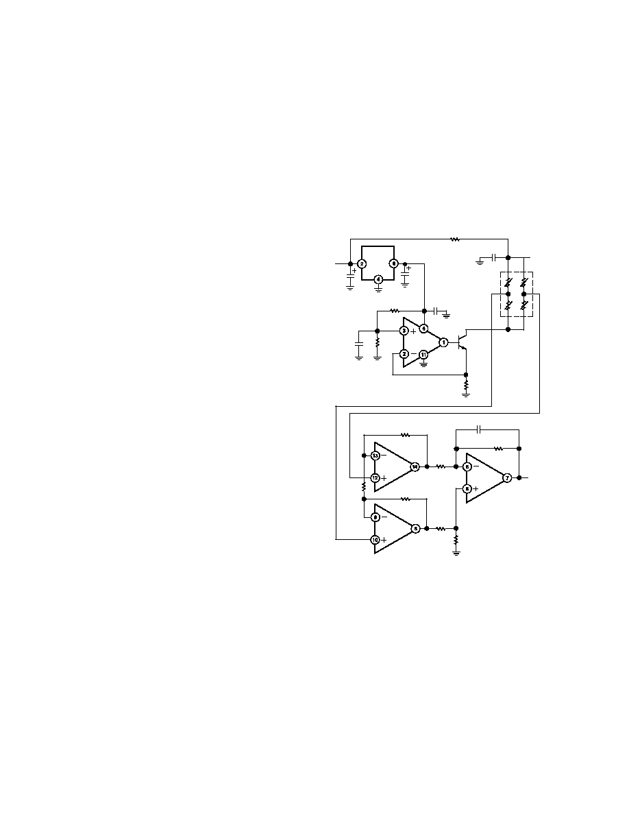
DICE CHARACTERISTICS
OUTPUT
6
OUTPUT
6
4
GND
3
SLEEP
2
V+
REF19x Die Size 0.041
×
0.057 Inch, 2,337 Sq. Mils
Substrate Is Connected to V+, Number of Transistors:
Bipolar 25, MOSFET4. Process: CBCMOS1
(@ I
LOAD
= 0 mA, T
A
= +25
°
C unless otherwise noted)
CAUTION
ESD (electrostatic discharge) sensitive device. Electrostatic charges as high as 4000 V readily
accumulate on the human body and test equipment and can discharge without detection.
Although the REF19x features proprietary ESD protection circuitry, permanent damage may
occur on devices subjected to high energy electrostatic discharges. Therefore, proper ESD
precautions are recommended to avoid performance degradation or loss of functionality.
WARNING!
ESD SENSITIVE DEVICE
REV. D
15
REF19x Series
5.004
4.996
100
4.998
4.997
25
50
5.000
4.999
5.001
5.002
5.003
75
50
25
0
TEMPERATURE C
OUTPUT VOLTAGE Volts
3 TYPICAL PARTS
5.15V < V
IN
< 15V
Figure 1. REF195 Output Voltage vs. Temperature
32
0
30
8
4
5
0
16
12
20
24
28
25
20
15
10
I
LOAD
mA
LINE REGULATION ppm/V
40 C
+25 C
+5.15V V
S
15V
+85 C
Figure 2. REF195 Line Regulation vs. I
LOAD
20
0
16
12
4
6
8
4
16
14
12
10
8
V
IN
Volts
LOAD REGULATION ppm/mA
+85 C
+25 C
40 C
O I
OUT
< 25mA
Figure 3. REF195 Load Regulation vs. V
IN
50
0
20
15
5
15
10
20
30
20
25
35
40
45
15
10
5
0
5
10
T
C
V
OUT
ppm/ C
PERCENTAGE OF PARTS %
40 C
T
A
+85 C
BASED ON 600
UNITS, 4 RUNS
Figure 4. T
C
V
OUT
Distribution
40
0
100
10
5
25
50
20
15
25
30
35
75
50
25
0
TEMPERATURE C
SUPPLY CURRENT
A
NORMAL MODE
SLEEP MODE
Figure 5. Quiescent Current vs. Temperature
6
0
100
3
1
25
2
50
5
4
75
50
25
0
TEMPERATURE C
SLEEP PIN CURRENT
A
V
L
V
H
Figure 6. SLEEP Pin Current vs. Temperature
REF19x Series
16
REV. D
10
100
1M
100k
10k
1k
60
40
20
0
120
100
80
FREQUENCY Hz
RIPPLE REJECTION dB
Figure 7a. Ripple Rejection vs. Frequency
REF19x
6
4
2
1k
REF
10 F
V
IN
= +15V
OUTPUT
1k
10 F
1 F
10 F
Figure 7b. Ripple Rejection vs. Frequency
Measurement Circuit
0
10
100
10M
1M
100k
10k
1k
1
2
3
4
FREQUENCY Hz
V
G
= 2V p-p
V
S
= 4.00V
V
IN
= 7V
REF19x
6
4
2
200
1 F
Z
1 F
I
O
Figure 8. Output Impedance vs. Frequency
100 s
20mV
5V
10
0%
90
ON
OFF
100
Figure 9a. Load Transient Response
V
IN
= 15V
0
10mA
6
REF19x
2
4
1 F
Figure 9b. Load Transient Response Measurement Circuit
10
100
0%
90
2V
2V
1mA
LOAD
30mA
LOAD
100 s
Figure 10a. Power ON Response Time
V
IN
= 7.0V
REF19x
2
4
6
1 F
Figure 10b. Power ON Response Time Measurement
Circuit
10
100
0%
90
1V
2ms
5V
ON
OFF
V
OUT
I
L
= 1mA
I
L
= 10mA
Figure 11a. Sleep Response Time
V
IN
= 15V
REF19x
V
OUT
6
2
4
3
1 F
Figure 11b. Sleep Response Time Measurement Circuit
REV. D
17
REF19x Series
35
0
0.9
15
5
0.1
10
0
30
20
25
0.8
0.7
0.6
0.5
0.4
0.3
0.2
REF195 DROPOUT VOLTAGE V
LOAD CURRENT mA
Figure 13. Dropout Voltage vs. Load Current
10
100
0%
90
5V
200mV
200 s
Figure 12. Line Transient Response
Output Voltage Bypassing
For stable operation, low dropout voltage regulators and refer-
ences, in general, require a bypass capacitor connected from
their V
OUT
pins to their GND pins. Although the REF19x
family of references is capable of stable operation with capacitive
loads exceeding 100
µ
F, a 1
µ
F capacitor is sufficient to guaran-
tee rated performance. The addition of a 0.1
µ
F ceramic ca-
pacitor in parallel with the bypass capacitor will improve load
current transient performance. For best line voltage transient
performance, it is recommended that the voltage inputs of these
devices be bypassed with a 10
µ
F electrolytic capacitor in paral-
lel with a 0.1
µ
F ceramic capacitor.
Sleep Mode Operation
All REF19x devices include a sleep capability that is TTL/CMOS
level compatible. Internal to the REF19x at the SLEEP pin, a
pull-up current source to V
IN
is connected. This permits the
SLEEP pin to be driven from an open collector/drain driver.
A logic LOW or a zero volt condition on the SLEEP pin is re-
quired to turn the output stage OFF. During sleep, the output
of the references becomes a high impedance state where its
potential would then be determined by external circuitry. If the
sleep feature is not used, it is recommended that the SLEEP pin
be connected to V
IN
(Pin 2).
Basic Voltage Reference Connections
The circuit in Figure 15 illustrates the basic configuration for
the REF19x family of references. Note the 10
µ
F/0.1
µ
F bypass
network on the input and the 1
µ
F/0.1
µ
F bypass network on the
output. It is recommended that no connections be made to
Pins 1, 5, 7 and 8. If the sleep feature is not required, Pin 3
should be connected to V
IN
.
NC
NC
V
IN
SLEEP
1
2
3
4
8
7
6
5
NC
NC
1 F
TANT
OUTPUT
0.1 F
10 F
0.1 F
REF19x
Figure 15. Basic Voltage Reference Configuration
+V
V
OUT
SHUTDOWN
GND
Figure 14. Simplified Schematic
APPLICATIONS SECTION
Output Short Circuit Behavior
The REF19x family of devices is totally protected from damage
due to accidental output shorts to GND or to V+. In the event
of an accidental short circuit condition, the reference device will
shutdown and limit its supply current to 100
µ
A.
Device Power Dissipation Considerations
The REF19x family of references is capable of delivering load
currents to 30 mA with an input voltage that ranges from 3.3 V
to 15 V. When these devices are used in applications with large
input voltages, care should be exercised to avoid exceeding these
devices' maximum internal power dissipation. Exceeding the
published specifications for maximum power dissipation or
junction temperature could result in premature device failure.
The following formula should be used to calculate a device's
maximum junction temperature or dissipation:
P
D
=
T
J
T
A
JA
In this equation, T
J
and T
A
are the junction and ambient tem-
peratures, respectively, P
D
is the device power dissipation and
JA
is the device package thermal resistance.
REF19x Series
18
REV. D
Membrane Switch Controlled Power Supply
With output load currents in the tens of mA, the REF19x family
of references can operate as a low dropout power supply in
hand-held instrument applications. In the circuit shown in
Figure 16, a membrane ON/OFF switch is used to control the
operation of the reference. During an initial power-on condi-
tion, the SLEEP pin is held to GND by the 10 k
resistor.
Recall that this condition disables (read: three-state) the
REF19x output. When the membrane ON switch is pressed,
the SLEEP pin is momentarily pulled to V
IN
, enabling the
REF19x output. At this point, current through the 10 k
is
reduced and the internal current source connected to the
SLEEP pin takes control. Pin 3 assumes and remains at the
same potential as V
IN
. When the membrane OFF switch is
pressed, the SLEEP pin is momentarily connected to GND,
which once again disables the REF19x output.
NC
NC
V
IN
1
2
3
4
8
7
6
5
NC
NC
OUTPUT
ON
OFF
10k
1k
5%
REF19x
1 F
TANT
Figure 16. Membrane Switch Controlled Power Supply
Current-Boosted References with Current Limiting
While the 30 mA rated output current of the REF19x series is
higher than typical of other reference ICs, it can be boosted to
higher levels if desired, with the addition of a simple external
PNP transistor, as shown in Figure 17. Full time current limit-
ing is used for protection of the pass transistor against shorts.
U1
REF196
(SEE TABLE)
R4
2
R1
1k
R2
1.5k
Q2
2N3906
C2
100 F/25V
D1
1N4148
(SEE TEXT
ON SLEEP)
R3
1.82k
C1
10 F/25V
(TANTALUM)
S
F
C3
0.1 F
F
S
R1
Q1
TIP32A
(SEE TEXT)
+V
S
= 6 TO 9V
(SEE TEXT)
V
S
COMMON
V
C
V
OUT
COMMON
OUTPUT TABLE
U1
REF192
REF193
REF196
REF194
REF195
V
OUT
(V)
2.5
3.0
3.3
4.5
5.0
+V
OUT
3.3V
@ 150mA
Figure 17. A Boosted 3.3 V Reference with Current
Limiting
In this circuit, the power supply current of reference U1 flowing
through R1R2 develops a base drive for Q1, whose collector
provides the bulk of the output current. With a typical gain of
100 in Q1 for 100 mA200 mA loads, U1 is never required to
furnish more than a few mA, so this factor minimizes tempera-
ture related drift. Short circuit protection is provided by Q2,
which clamps drive to Q1 at about 300 mA of load current with
values as shown. With this separation of control and power
functions, dc stability is optimum, allowing best advantage use
of premium grade REF19x devices for U1. Of course, load
management should still be exercised. A short, heavy, low DCR
(DC Resistance) conductor should be used from U16 to the
V
OUT
sense point "S," where the collector of Q1 connects to the
load, point "F."
Because of the current limiting configuration, the dropout volt-
age circuit is raised about 1.1 V over that of the REF19x de-
vices, due to the V
BE
of Q1 and the drop across current sense
resistor R4. However, overall dropout is typically still low
enough to allow operation of a 5 V to 3.3 V regulator/reference
using the REF196 for U1 as noted, with a V
S
as low as 4.5 V
and a load current of 150 mA.
The requirement for a heat sink on Q1 depends on the maxi-
mum input voltage and short circuit current. With V
S
= 5 V
and a 300 mA current limit, the worst case dissipation of Q1 is
1.5 W, less than the TO-220 package 2 W limit. However, if
smaller TO-39 or TO-5 packaged devices such as the 2N4033
are used, the current limit should be reduced to keep maximum
dissipation below the package rating. This is accomplished by
simply raising R 4.
A tantalum output capacitor is used at C1 for its low ESR
(Equivalent Series Resistance), and the higher value is required
for stability. Capacitor C2 provides input bypassing and can be
an ordinary electrolytic.
Shutdown control of the booster stage is shown as an option,
and when used some cautions are in order. Because of the
additional active devices in the V
S
line to U1, direct drive to
Pin 3 does not work as with an unbuffered REF19x device. To
enable shutdown control, the connection to U1-2 is broken at
the "X," and diode D1 then allows a CMOS control source V
C
to drive U1-3 for ON-OFF operation. Startup from shutdown is
not as clean under heavy load as it is in basic REF19x series and
can require several milliseconds under load. Nevertheless, it is
still effective and can fully control 150 mA loads. When shutdown
control is used, heavy capacitive loads should be minimized.
REV. D
19
REF19x Series
A Negative Precision Reference without Precision Resistors
In many current-output CMOS DAC applications, where the
output signal voltage must be of the same polarity as the
reference voltage, it is often required to reconfigure a cur-
rent-switching DAC into a voltage-switching DAC through the
use of a 1.25 V reference, an op amp and a pair of resistors.
Using a current-switching DAC directly requires an additional
operational amplifier at the output to reinvert the signal. A
negative voltage reference is then desirable from the point that
an additional operational amplifier is not required for either
reinversion (current-switching mode) or amplification (voltage
switching mode) of the DAC output voltage. In general, any
positive voltage reference can be converted into a negative volt-
age reference through the use of an operational amplifier and a
pair of matched resistors in an inverting configuration. The
disadvantage to that approach is that the largest single source of
error in the circuit is the relative matching of the resistors used.
The circuit illustrated in Figure 18 avoids the need for tightly
matched resistors with the use of an active integrator circuit. In
this circuit, the output of the voltage reference provides the
input drive for the integrator. The integrator, to maintain cir-
cuit equilibrium, adjusts its output to establish the proper rela-
tionship between the reference's V
OUT
and GND. Thus, any
desired negative output voltage can be chosen by simply sub-
stituting for the appropriate reference IC. The sleep feature is
maintained in the circuit with the simple addition of a PNP
transistor and a 10 k
resistor. One caveat with this approach
should be mentioned: although rail-to-rail output amplifiers
work best in the application, these operational amplifiers require
a finite amount (mV) of headroom when required to provide
any load current. The choice for the circuit's negative supply
should take this issue into account.
A1
+5V
5V
100
1 F
1k
1 F
V
REF
100k
REF19x
V
IN
GND
V
REF
SLEEP
10k
SLEEP
TTL/CMOS
A1 = 1/2 OP295,
1/2 OP291
V
IN
10k
2N3906
Figure 18. A Negative Precision Voltage Reference
Uses No Precision Resistors
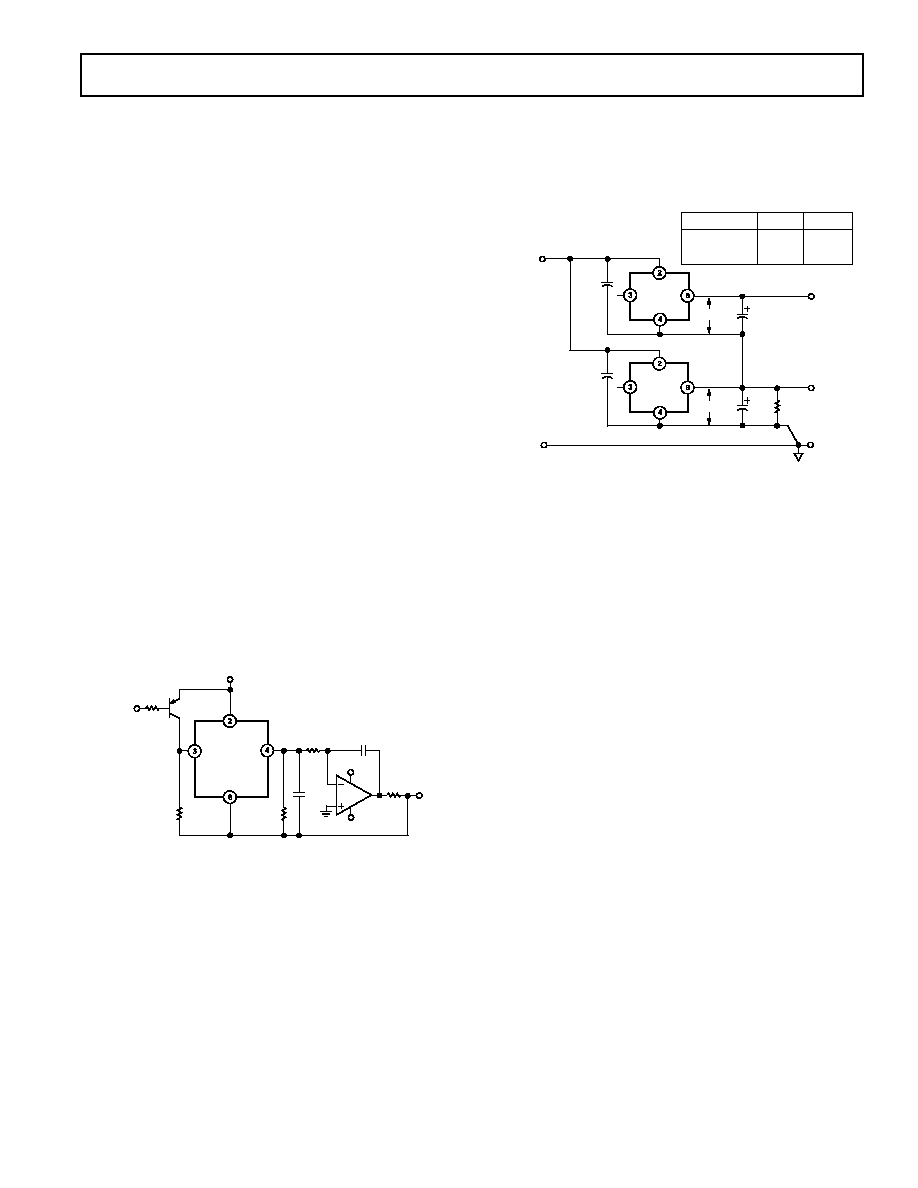
Stacking Reference ICs for Arbitrary Outputs
Some applications may require two reference voltage sources
that are a combined sum of standard outputs. The circuit of
Figure 19 shows how this "stacked output" reference can be
implemented.
U2
REF19x
(SEE TABLE)
R1
3.9k
(SEE TEXT)
C1
0.1 F
+V
S
V
S
> V
OUT2
+0.15V
V
IN
COMMON
V
OUT
COMMON
OUTPUT TABLE
U1/U2
REF192/REF192
REF192/REF194
REF192/REF195
V
OUT1
(V)
2.5
2.5
2.5
V
OUT2
(V)
5.0
7.0
7.5
+V
OUT2
V
O
(U2)
C2
1 F
C3
0.1 F
+V
OUT1
V
O
(U1)
C4
1 F
U1
REF19x
(SEE TABLE)
Figure 19. Stacking Voltage References with the REF19x
Two reference ICs are used, fed from a common unregulated
input, V
S
. The outputs of the individual ICs are simply con-
nected in series as shown, which provides two output voltages,
V
OUT1
and V
OUT2
. V
OUT1
is the terminal voltage of U1, while
V
OUT2
is the sum of this voltage and the terminal voltage of U2.
U1 and U2 are simply chosen for the two voltages that supply
the required outputs (see table). If, for example, both U1 and
U2 are REF192s, the two outputs are 2.5 V and 5.0 V.
While this concept is simple, some cautions are in order. Since
the lower reference circuit must sink a small bias current from
U2 (50
µ
A100
µ
A), plus the base current from the series PNP
output transistor in U2, either the external load of U1 or R1
must provide a path for this current. If the U1 minimum load is
not well defined, resistor R1 should be used, set to a value that
will conservatively pass 600
µ
A of current with the applicable
V
OUT1
across it. Note that the two U1 and U2 reference circuits
are locally treated as macrocells, each having its own bypasses at
input and output for best stability. Both U1 and U2 in this
circuit can source dc currents up to their full rating. The mini-
mum input voltage, V
S
, is determined by the sum of the out-
puts, V
OUT2
, plus the dropout voltage of U2.
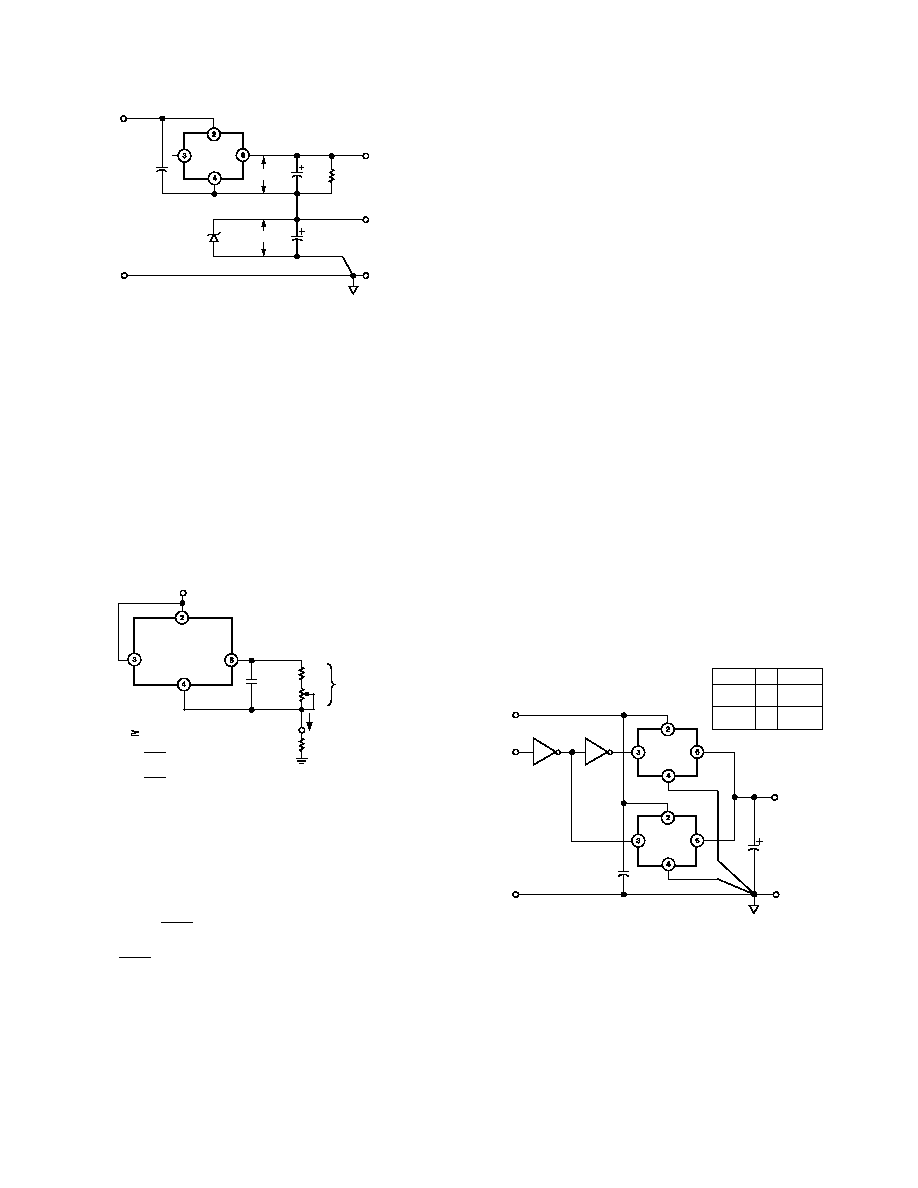
A related variation on stacking two three-terminal references is
shown in Figure 19, where U1, a REF192, is stacked with a
two-terminal reference diode such as the AD589. Like the
three-terminal stacked reference above, this circuit provides two
outputs, V
OUT1
and V
OUT2
, which are the individual terminal
voltages of D1 and U1 respectively. Here this is 1.235 and 2.5,
which provides a V
OUT2
of 3.735 V. When using two-terminal
reference diodes such as D1, the rated minimum and maximum
device currents must be observed and the maximum load cur-
rent from V
OUT1
can be no greater than the current set up by R1
and V
O(U1)
. In the case with V
O(U1)
equal to 2.5 V, R1 provides
a 500
µ
A bias to D1, so the maximum load current available at
V
OUT1
is 450
µ
A or less.
REF19x Series
20
REV. D
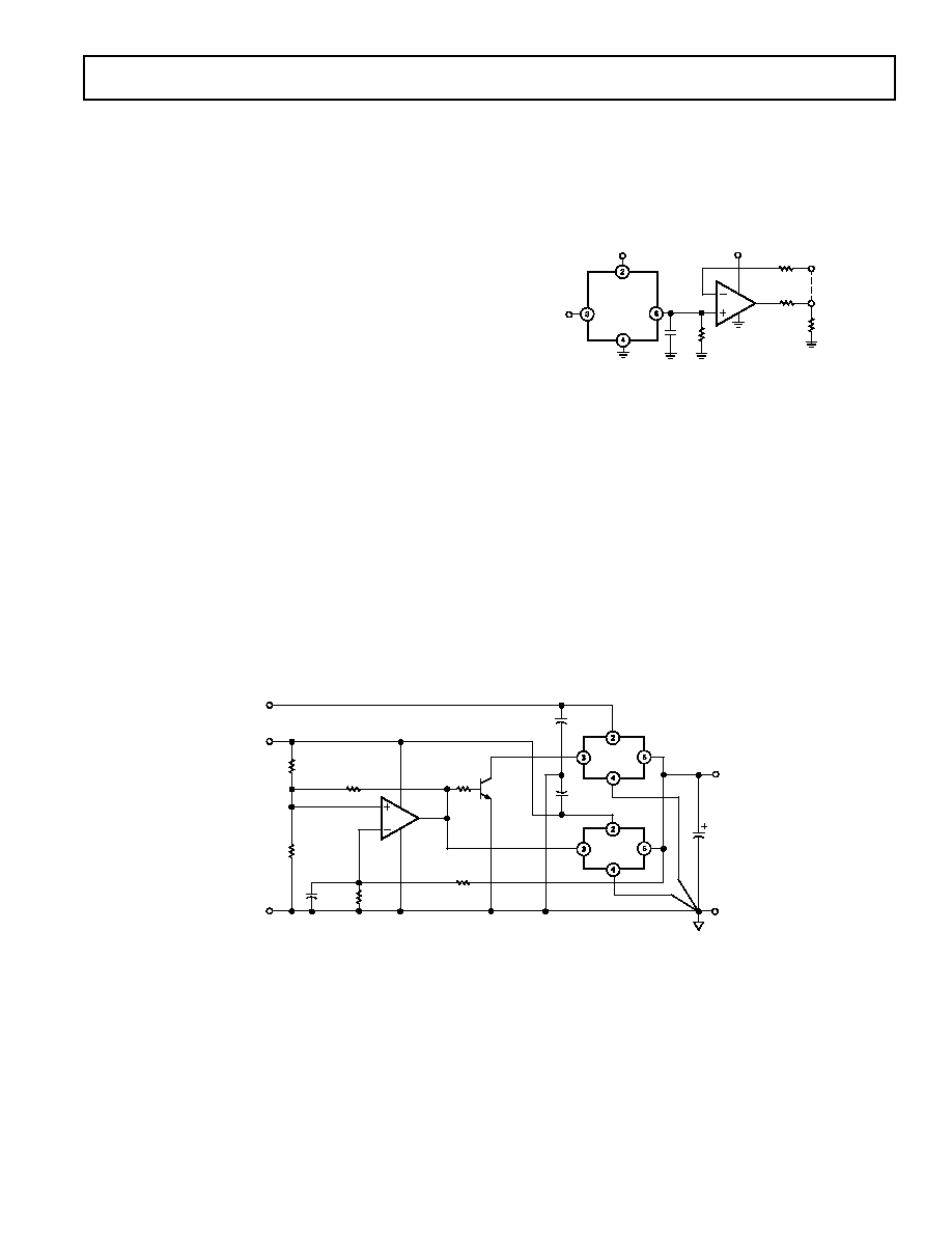
Switched Output 5 V/3.3 V Reference
Applications often require digital control of reference voltages,
selecting between one stable voltage and a second. With the
sleep feature inherent to the REF19x series, switched output
reference configurations are easily implemented with relatively
little additional hardware.
The circuit of Figure 22 illustrates the general technique, which
takes advantage of the output "wire-OR" capability of the
REF19x device family. When OFF, a REF19x device is effec-
tively an open circuit at the output node with respect to the
power supply. When ON, a REF19x device can source current
up to its current rating, but sink only a few
µ
A (essentially just
the relatively low current of the internal output scaling divider).
As a result, for two devices wired together at their common
outputs, the output voltage is simply that of the ON device.
The OFF state device will draw a small standby current of
15
µ
A (max), but otherwise will not interfere with operation of
the ON device, which can operate to its full current rating.
Note that the two devices in the circuit conveniently share
both input and output capacitors, and with CMOS logic
drive, it is power efficient.
Using dissimilar REF19x series devices with this configuration
allows logic selection between the U1/U2 specified terminal
voltages. For example, with U1 (a REF195) and U2 (a REF196),
as noted in the table, changing the CMOS compatible V
C
logic
control voltage from HI to LO selects between a nominal output
of 5.000 V and 3.300 V and vice versa. Other REF19x family
units can also be used for U1/U2, with similar operation in a
logic sense, but with outputs as per the individual paired devices
(see table, again). Of course, the exact output voltage tolerance,
drift and overall quality of the reference voltage will be consis-
tent with the grade of individual U1 and U2 devices.
U1
REF19x
(SEE TABLE)
C1
0.1 F
+V
S
= 6V
V
IN
COMMON
V
OUT
COMMON
+V
OUT
C2
1 F
U2
REF19x
(SEE TABLE)
3
4
1
2
U3B
74HC04
U3A
74HC04
V
C
OUTPUT TABLE
V
OUT
(V)
5.0
3.3
4.5
5.0
V
C
*
HI
LO
HI
LO
U1/U2
REF195/
REF196
REF194/
REF195
* CMOS LOGIC LEVELS
Figure 22. Switched Output Reference
U1
REF192
R1
4.99k
(SEE TEXT)
C1
0.1 F
+V
S
V
S
> V
OUT2
+0.15V
V
IN
COMMON
V
OUT
COMMON
+V
OUT2
3.735V
V
O
(U1)
C2
1 F
D1
AD589
V
O
(D1)
C3
1 F
+V
OUT1
1.235V
Figure 20. Stacking Voltage References with the REF19x
A Precision Current Source
Many times, in low power applications, the need arises for a
precision current source that can operate on low supply volt-
ages. As shown in Figure 21, any one of the devices in the
REF19x family of references can be configured as a precision
current source. The circuit configuration illustrated is a floating
current source with a grounded load. The reference's output
voltage is bootstrapped across R
SET
, which sets the output cur-
rent into the load. With this configuration, circuit precision is
maintained for load currents in the range from the reference's
supply current (typically, 30
µ
A) to approximately 30 mA. The
low dropout voltage of these devices maximizes the current
source's output voltage compliance without excess headroom.
1 F
REF19x
V
IN
GND
V
REF
SLEEP
V
IN
I
SY
ADJUST
R1
P1
R
L
R
SET
I
OUT
V
IN
I
OUT
· R
L
(MAX) + V
SY
(MIN)
I
OUT
= + I
SY
(REF19x)
R
SET
V
OUT
R
SET
V
OUT
>> I
SY
E.G. REF195 : V
OUT
= 5V
I
OUT
= 5mA
R1 = 953
P1 = 100 , 10-TURN
Figure 21. A Low Dropout, Precision Current Source
The circuit's governing equations are:
V
IN
=
I
OUT
×
R
L
(max )
+
V
SY
(min, REF19x)
I
OUT
=
V
OUT
R
SET
+
I
SY
(REF19x)
V
OUT
R
SET
I
SY
(REF19x)
REV. D
21
REF19x Series
resistance within the forcing loop of the op amp. Since the op
amp senses the load voltage, op amp loop control forces the
output to compensate for the wiring error and to produce the
correct voltage at the load. Depending on the reference device
chosen, operational amplifiers that can be used in this applica-
tion are the OP295, the OP291 and the OP183/OP283.
1 F
REF19x
V
IN
GND
V
OUT
V
IN
100k
R
L
R
LW
SLEEP
V
IN
2
3
1
A1
R
LW
+V
OUT
SENSE
+V
OUT
FORCE
A1 = 1/2 OP295
1/2 OP292
1/2 OP283
Figure 23. A Low Dropout, Kelvin Connected Voltage
Reference
A Fail-Safe 5 V Reference
Some critical applications require a reference voltage to be
maintained constant, even with a loss of primary power. The
low standby power of the REF19x series and the switched out-
put capability allow a "fail-safe" reference configuration to be
implemented rather easily. This reference maintains a tight
output voltage tolerance for either a primary power source (ac
line derived) or a standby (battery derived) power source, auto-
matically switching between the two as the power conditions
change.
The circuit in Figure 24 illustrates the concept, which borrows
from the switched output idea of Figure 21, again using the
REF19x device family output "wire-OR" capability. In this
case, since a constant 5 V reference voltage is desired for all
There is one application caveat that should be understood about
this circuit, which comes about due to the wire-OR nature.
Since U1 and U2 can only source current effectively, negative
going output voltage changes, which require the sinking of cur-
rent, will necessarily take longer than positive going changes. In
practice, this means that the circuit is quite fast when undergo-
ing a transition from 3.3 to 5 V, but the transition from 5 to
3.3 V will take longer. Exactly how much longer will be a func-
tion of the load resistance, R
L
,
seen at the output and the
typical 1
µ
F value of C2. In general, a conservative transition
time here will be on the order of several milliseconds for load
resistances in the range of 100
1 k
. Note that for highest
accuracy at the new output voltage, several time constants
should be allowed (>7.6 time constants for <1/2 LSB error @
10 bits, for example).
Kelvin Connections
In many portable instrumentation applications where PC board
cost and area go hand-in-hand, circuit interconnects are very
often of dimensionally minimum width. These narrow lines can
cause large voltage drops if the voltage reference is required to
provide load currents to various functions. In fact, a circuit's
interconnects can exhibit a typical line resistance of 0.45 m
/
square (1 oz. Cu, for example). In those applications where
these devices are configured as low dropout voltage regulators,
these wiring voltage drops can become a large source of error.
To circumvent this problem, force and sense connections can be
made to the reference through the use of an operational ampli-
fier, as shown in Figure 23. This method provides a means by
which the effects of wiring resistance voltage drops can be elimi-
nated. Load currents flowing through wiring resistance produce
an I-R error (I
LOAD
×
R
WIRE
) at the load. However, the Kelvin
connection overcomes the problem by including the wiring
U1
REF195
C1
0.1 F
V
S
, V
BAT
COMMON
V
OUT
COMMON
+5.000V
C3
1 F
U2
REF195
R5
100k
R6
100
C2
0.1 F
6
4
2
3
U3
AD820
R4
900k
C4
0.1 F
R2
100k
R3
10M
R1
1.1M
+V
BAT
+V
S
Q1
2N3904
7
Figure 24. A Fail-Safe 5 V Reference
REF19x Series
22
REV. D
conditions, two REF195 devices are used for U1 and U2, with
their ON/OFF switching controlled by the presence or absence
of the primary dc supply source, V
S
. V
BAT
is a 6 V battery
backup source that supplies power to the load only when V
S
fails. For normal (V
S
present) power conditions, V
BAT
sees only
the 15
µ
A (max) standby current drain of U1 in its OFF state.
In operation, it is assumed that for all conditions either U1 or
U2 is ON and a 5 V reference output is available. With this
voltage constant, a scaled down version is applied to the com-
parator IC U3, providing a fixed 0.5 V input to the () input for
all power conditions. The R1R2
divider provides a signal to
the U3 (+) input proportional to V
S
, which switches U3 and
U1/U2 dependent upon the absolute level of V
S
. Op amp U3 is
configured here as a comparator with hysteresis, which provides
for clean, noise free output switching. This hysteresis is impor-
tant to eliminate rapid switching at the threshold due to V
S
ripple. Further, the device chosen is the AD820, a rail-rail
output device, which provides HI and LO output states within a
few mV of V
S
and ground for accurate thresholds and compat-
ible drive for U2 for all V
S
conditions. R3 provides positive
feedback for circuit hysteresis, changing the threshold at the (+)
input as a function of U3's output.
For V
S
levels lower than the LOWER threshold, U3's output is
low, thus U2 and Q1 are OFF, while U1 is ON. For V
S
levels
higher than the UPPER threshold, the situation reverses, with
U1 OFF and both U2 and Q1 ON. In the interest of battery
power conservation, all of the comparison switching circuitry is
powered from V
S
and is so arranged that when V
S
fails the de-
fault output comes from U1.
For the R1R3
values as shown, the LOWER/UPPER V
S
switching thresholds are approximately 5.5 V and 6 V, respec-
tively. These can obviously be changed to suit other V
S
sup-
plies, as can the REF19x devices used for U1 and U2, over a
range of 2.5 V to 5 V of output. U3 can operate down to a V
S
of 3.3 V, which is generally compatible with all family devices.
A Low Power, Strain Gage Circuit
As shown in Figure 25, the REF19x family of references can
be used in conjunction with low supply voltage operational
amplifiers, such as the OP492 and the OP283, in a self-con-
tained strain gage circuit. In this circuit, the REF195 was used
as the core of this low power, strain gage circuit. Other refer-
ences can be easily accommodated by changing circuit element
values. The references play a dual role as the voltage regulator
to provide the supply voltage requirements of the strain gage
and the operational amplifiers as well as a precision voltage
reference for the current source used to stimulate the bridge. A
distinct feature of the circuit is that it can be remotely controlled
ON or OFF by digital means via the SLEEP pin.
500
0.1%
57k
1%
0.1 F
10k
1%
0.1 F
1/4
OP492
10 F
1 F
REF195
1/4
OP492
1/4
OP492
1/4
OP492
2.21k
20k
1%
10k
1%
20k
1%
20k
1%
0.01 F
10 F
100
OUTPUT
2N2222
20k
1%
10k
1%
Figure 25. A Low Power, Strain Gage Circuit
REV. D
23
REF19x Series
OUTLINE DIMENSIONS
Dimensions shown in inches and (mm).
8-Lead Plastic DIP (P Suffix)
(N-8)
8
1
4
5
0.430 (10.92)
0.348 (8.84)
0.280 (7.11)
0.240 (6.10)
PIN 1
SEATING
PLANE
0.022 (0.558)
0.014 (0.356)
0.060 (1.52)
0.015 (0.38)
0.210 (5.33)
MAX
0.130
(3.30)
MIN
0.070 (1.77)
0.045 (1.15)
0.100
(2.54)
BSC
0.160 (4.06)
0.115 (2.93)
0.325 (8.25)
0.300 (7.62)
0.015 (0.381)
0.008 (0.204)
0.195 (4.95)
0.115 (2.93)
8-Lead Narrow Body SO (S Suffix)
(SO-8)
0.1968 (5.00)
0.1890 (4.80)
8
5
4
1
0.2440 (6.20)
0.2284 (5.80)
PIN 1
0.1574 (4.00)
0.1497 (3.80)
0.0688 (1.75)
0.0532 (1.35)
SEATING
PLANE
0.0098 (0.25)
0.0040 (0.10)
0.0192 (0.49)
0.0138 (0.35)
0.0500
(1.27)
BSC
0.0098 (0.25)
0.0075 (0.19)
0.0500 (1.27)
0.0160 (0.41)
8
°
0
°
0.0196 (0.50)
0.0099 (0.25)
x 45
°
8-Lead TSSOP (RU Suffix)
(RU-8)
8
5
4
1
0.122 (3.10)
0.114 (2.90)
0.256 (6.50)
0.246 (6.25)
0.177 (4.50)
0.169 (4.30)
PIN 1
0.0256 (0.65)
BSC
SEATING
PLANE
0.006 (0.15)
0.002 (0.05)
0.0118 (0.30)
0.0075 (0.19)
0.0433
(1.10)
MAX
0.0079 (0.20)
0.0035 (0.090)
0.028 (0.70)
0.020 (0.50)
8
°
0
°
PRINTED IN U.S.A.
C1951d23/99