 | ÐлекÑÑоннÑй компоненÑ: SALEM3T | СкаÑаÑÑ:  PDF PDF  ZIP ZIP |
/home/web/htmldatasheet/RUSSIAN/html/ad/195949
REV. B
Information furnished by Analog Devices is believed to be accurate and
reliable. However, no responsibility is assumed by Analog Devices for its
use, nor for any infringements of patents or other rights of third parties
which may result from its use. No license is granted by implication or
otherwise under any patent or patent rights of Analog Devices.
a
ADSP-21065L
One Technology Way, P.O. Box 9106, Norwood, MA 02062-9106, U.S.A.
Tel: 781/329-4700
World Wide Web Site: http://www.analog.com
Fax: 781/326-8703
© Analog Devices, Inc., 2000
DSP Microcomputer
SUMMARY
High Performance Signal Computer for Communica-
tions, Audio, Automotive, Instrumentation and
Industrial Applications
Super Harvard Architecture Computer (SHARC
®
)
Four Independent Buses for Dual Data, Instruction,
and I/O Fetch on a Single Cycle
32-Bit Fixed-Point Arithmetic; 32-Bit and 40-Bit Floating-
Point Arithmetic
544 Kbits On-Chip SRAM Memory and Integrated I/O
Peripheral
I
2
S Support, for Eight Simultaneous Receive and Trans-
mit Channels
KEY FEATURES
66 MIPS, 198 MFLOPS Peak, 132 MFLOPS Sustained
Performance
User-Configurable 544 Kbits On-Chip SRAM Memory
Two External Port, DMA Channels and Eight Serial
Port, DMA Channels
SDRAM Controller for Glueless Interface to Low Cost
External Memory (@ 66 MHz)
64M Words External Address Range
12 Programmable I/O Pins and Two Timers with Event
Capture Options
Code-Compatible with ADSP-2106x Family
208-Lead MQFP or 196-Ball Mini-BGA Package
3.3 Volt Operation
Flexible Data Formats and 40-Bit Extended Precision
32-Bit Single-Precision and 40-Bit Extended-Precision IEEE
Floating-Point Data Formats
32-Bit Fixed-Point Data Format, Integer and Fractional,
with Dual 80-Bit Accumulators
Parallel Computations
Single-Cycle Multiply and ALU Operations in Parallel with
Dual Memory Read/Writes and Instruction Fetch
Multiply with Add and Subtract for Accelerated FFT But-
terfly Computation
1024-Point Complex FFT Benchmark: 0.274 ms (18,221
Cycles)
SPORT 1
4
IOP
REGISTERS
(MEMORY MAPPED)
CONTROL,
STATUS, TIMER
&
DATA BUFFERS
I/O PROCESSOR
INSTRUCTION
CACHE
32 48 BIT
DATA
ADDR
TWO INDEPENDENT
DUAL-PORTED BLOCKS
PROCESSOR PORT
I/O PORT
BLOCK 0
BLOCK 1
JTAG
TEST &
EMULATION
7
HOST PORT
ADDR BUS
MUX
IOA
17
IOD
48
MULTIPROCESSOR
INTERFACE
DUAL-PORTED SRAM
EXTERNAL
PORT
DATA BUS
MUX
32
24
24
PM ADDRESS BUS
DM ADDRESS BUS
PM DATA BUS
DM DATA BUS
BUS
CONNECT
(PX)
DATA
REGISTER
FILE
16 40 BIT
BARREL
SHIFTER
ALU
MULTIPLIER
32
48
40
CORE PROCESSOR
DMA
CONTROLLER
PROGRAM
SEQUENCER
DAG2
8 4 24
SDRAM
INTERFACE
(I
2
S)
(2 Rx, 2Tx)
(2 Rx, 2Tx)
(I
2
S)
SPORT 0
DAG1
8 4 32
DATA
DATA
DATA
ADDR
ADDR
ADDR
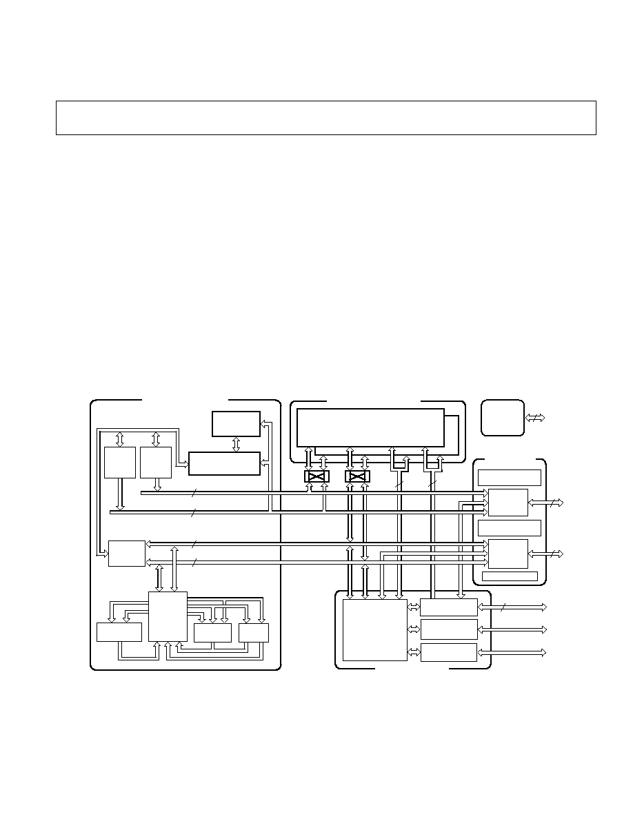
Figure 1. Functional Block Diagram
SHARC is a registered trademark of Analog Devices, Inc.

REV. B
ADSP-21065L
2
544 Kbits Configurable On-Chip SRAM
Dual-Ported for Independent Access by Core Processor
and DMA
Configurable in Combinations of 16-, 32-, 48-Bit Data and
Program Words in Block 0 and Block 1
DMA Controller
Ten DMA Channels--Two Dedicated to the External Port
and Eight Dedicated to the Serial Ports
Background DMA Transfers at up to 66 MHz, in Parallel
with Full Speed Processor Execution
Performs Transfers Between:
Internal RAM and Host
Internal RAM and Serial Ports
Internal RAM and Master or Slave SHARC
Internal RAM and External Memory or I/O Devices
External Memory and External Devices
Host Processor Interface
Efficient Interface to 8-, 16-, and 32-Bit Microprocessors
Host Can Directly Read/Write ADSP-21065L IOP Registers
Multiprocessing
Distributed On-Chip Bus Arbitration for Glueless, Parallel
Bus Connect Between Two ADSP-21065Ls Plus Host
132 Mbytes/s Transfer Rate Over Parallel Bus
Serial Ports
Independent Transmit and Receive Functions
Programmable 3-Bit to 32-Bit Serial Word Width
I
2
S Support Allowing Eight Transmit and Eight Receive
Channels
Glueless Interface to Industry Standard Codecs
TDM Multichannel Mode with -Law/A-Law Hardware
Companding
Multichannel Signaling Protocol
REV. B
ADSP-21065L
3
GENERAL DESCRIPTION
The ADSP-21065L is a powerful member of the SHARC
family of 32-bit processors optimized for cost sensitive appli-
cations. The SHARC--Super Harvard Architecture--offers the
highest levels of performance and memory integration of any
32-bit DSP in the industry--they are also the only DSP in the
industry that offer both fixed and floating-point capabilities,
without compromising precision or performance.
Fabricated in a high speed, low power CMOS process, 0.35
µm
technology, the ADSP-21065L offers the highest performance
by a 32-bit DSP--66 MIPS (198 MFLOPS). With its on-chip
instruction cache, the processor can execute every instruction in
a single cycle. Table I lists the performance benchmarks for the
ADSP-21065L.
The ADSP-21065L SHARC combines a floating-point DSP
core with integrated, on-chip system features, including a
544 Kbit SRAM memory, host processor interface, DMA con-
troller, SDRAM controller, and enhanced serial ports.
Figure 1 shows a block diagram of the ADSP-21065L, illustrat-
ing the following architectural features:
Computation Units (ALU, Multiplier, and Shifter) with a
Shared Data Register File
Data Address Generators (DAG1, DAG2)
Program Sequencer with Instruction Cache
Timers with Event Capture Modes
On-Chip, dual-ported SRAM
External Port for Interfacing to Off-Chip Memory and
Peripherals
Host Port and SDRAM Interface
DMA Controller
Enhanced Serial Ports
JTAG Test Access Port
Table I. Performance Benchmarks
Benchmark
Timing
Cycles
Cycle Time
15.00 ns
1
1024-Pt. Complex FFT
(Radix 4, with Digit Reverse)
0.274 ns
18221
Matrix Multiply (Pipelined)
[3
× 3] × [3 × 1]
135 ns
9
[4
× 4] × [4 × 1]
240 ns
16
FIR Filter (per Tap)
15 ns
1
IIR Filter (per Biquad)
60 ns
4
Divide Y/X
90 ns
6
Inverse Square Root (1/
x)
135 ns
9
DMA Transfers
264 Mbytes/sec.
ADSP-21000 FAMILY CORE ARCHITECTURE
The ADSP-21065L is code and function compatible with the
ADSP-21060/ADSP-21061/ADSP-21062. The ADSP-21065L
includes the following architectural features of the SHARC
family core.
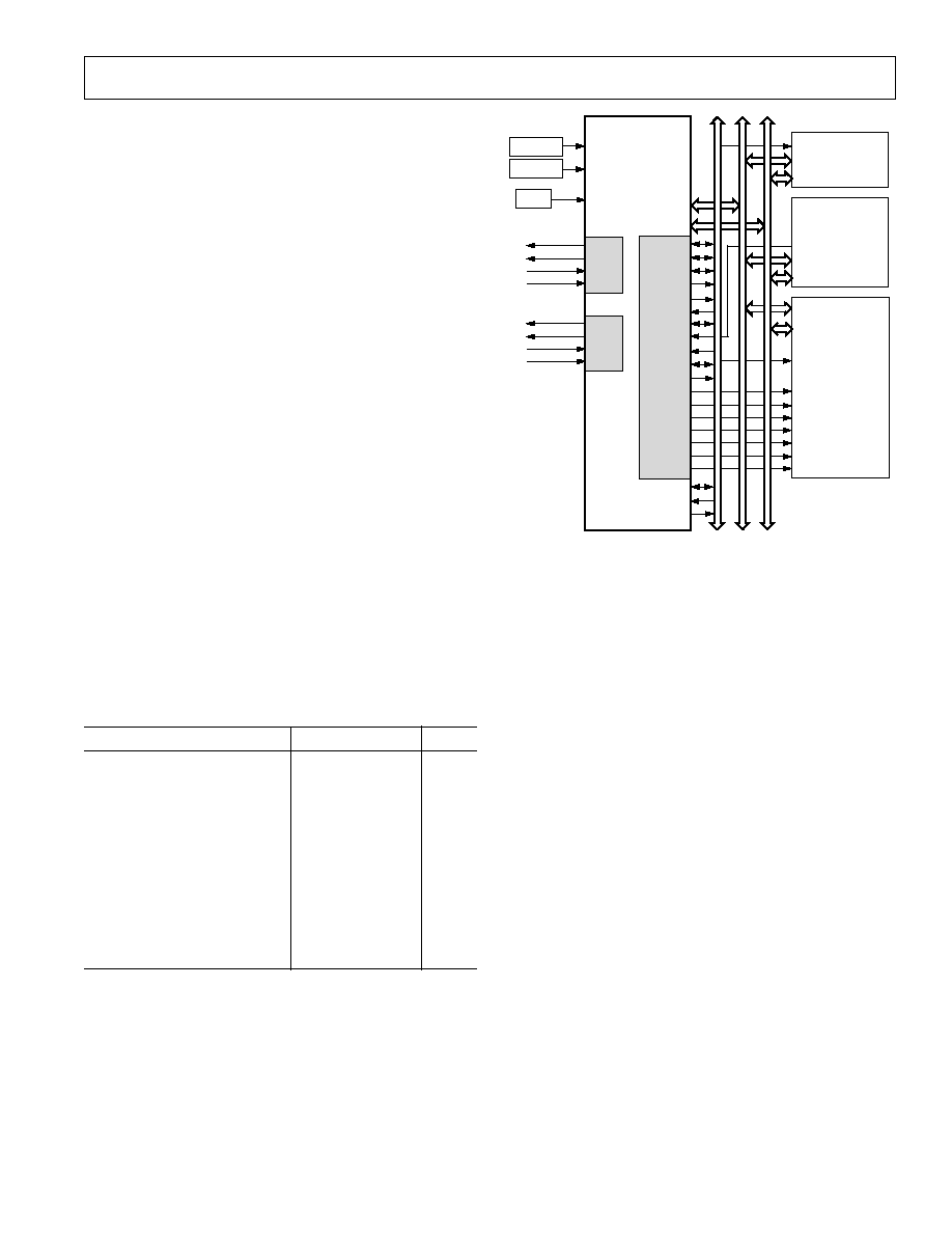
RESET
ADSP-21065L
#1
BMS
ADDR
23-0
DATA
31-0
CONTROL
ADDRESS
DATA
CS
ADDR
DATA
BOOT
EPROM
(OPTIONAL)
ADDR
SDRAM
(OPTIONAL)
DATA
ADDR
DATA
HOST
PROCESSOR
(OPTIONAL)
CLOCK
CS
HBR
HBG
REDY
RD
WR
ACK
SBTS
SW
BR
2
CLKIN
MS
3-0
CPA
CS
RESET
ID
1-0
01
TX0_A
TX0_B
RX0_A
RX0_B
SPORT0
TX1_A
TX1_B
RX1_A
RX1_B
SPORT1
CS
RAS
CAS
DQM
SDCLK
1-0
SDCKE
SDA10
BR
1
RAS
CAS
DQM
CLK
CKE
A10
CONTROL
SDWE
WE
Figure 2. ADSP-21065L Single-Processor System
Independent, Parallel Computation Units
The arithmetic/logic unit (ALU), multiplier, and shifter all
perform single-cycle instructions. The three units are arranged
in parallel, maximizing computational throughput. Single multi-
function instructions execute parallel ALU and multiplier
operations. These computation units support IEEE 32-bit
single-precision floating-point, extended precision 40-bit floating-
point, and 32-bit fixed-point data formats.
Data Register File
A general-purpose data register file is used for transferring data
between the computation units and the data buses, and for
storing intermediate results. This 10-port, 32-register (16 pri-
mary, 16 secondary) register file, combined with the ADSP-
21000 Harvard architecture, allows unconstrained data flow
between computation units and internal memory.
Single-Cycle Fetch of Instruction and Two Operands
The ADSP-21065L features an enhanced Super Harvard Archi-
tecture in which the data memory (DM) bus transfers data and
the program memory (PM) bus transfers both instructions and
data (see Figure 1). With its separate program and data memory
buses, and on-chip instruction cache, the processor can simulta-
neously fetch two operands and an instruction (from the cache),
all in a single cycle.
Instruction Cache
The ADSP-21065L includes an on-chip instruction cache that
enables three-bus operation for fetching an instruction and two
data values. The cache is selective--only the instructions that
fetches conflict with PM bus data accesses are cached. This
allows full-speed execution of core, looped operations such as
digital filter multiply-accumulates and FFT butterfly processing.
Data Address Generators with Hardware Circular Buffers
The ADSP-21065L's two data address generators (DAGs)
implement circular data buffers in hardware. Circular buffers
allow efficient programming of delay lines and other data

REV. B
ADSP-21065L
4
structures required in digital signal processing, and are com-
monly used in digital filters and Fourier transforms. The
ADSP-21065L's two DAGs contain sufficient registers to allow
the creation of up to 32 circular buffers (16 primary register
sets, 16 secondary). The DAGs automatically handle address
pointer wraparound, reducing overhead, increasing perfor-
mance, and simplifying implementation. Circular buffers can
start and end at any memory location.
Flexible Instruction Set
The 48-bit instruction word accommodates a variety of parallel
operations, for concise programming. For example, the ADSP-
21065L can conditionally execute a multiply, an add, a subtract
and a branch, all in a single instruction.
ADSP-21065L FEATURES
The ADSP-21065L is designed to achieve the highest system
throughput to enable maximum system performance. It can be
clocked by either a crystal or a TTL-compatible clock signal.
The ADSP-21065L uses an input clock with a frequency equal
to half the instruction rate--a 33 MHz input clock yields a
15 ns processor cycle (which is equivalent to 66 MHz). Inter-
faces on the ADSP-21065L operate as shown below. Hereafter
in this document, 1x = input clock frequency, and 2x = processor's
instruction rate.
The following clock operation ratings are based on 1x = 33 MHz
(instruction rate/core = 66 MHz):
SDRAM
66 MHz
External SRAM
33 MHz
Serial Ports
33 MHz
Multiprocessing
33 MHz
Host (Asynchronous)
33 MHz
Augmenting the ADSP-21000 family core, the ADSP-21065L
adds the following architectural features:
Dual-Ported On-Chip Memory
The ADSP-21065L contains 544 Kbits of on-chip SRAM,
organized into two banks: Bank 0 has 288 Kbits, and Bank 1 has
256 Kbits. Bank 0 is configured with 9 columns of 2K
× 16 bits,
and Bank 1 is configured with 8 columns of 2K
× 16 bits. Each
memory block is dual-ported for single-cycle, independent ac-
cesses by the core processor and I/O processor or DMA control-
ler. The dual-ported memory and separate on-chip buses allow
two data transfers from the core and one from I/O, all in a
single cycle (see Figure 4 for the ADSP-21065L Memory Map).
On the ADSP-21065L, the memory can be configured as a
maximum of 16K words of 32-bit data, 34K words for 16-bit
data, 10K words of 48-bit instructions (and 40-bit data) or
combinations of different word sizes up to 544 Kbits. All the
memory can be accessed as 16-bit, 32-bit or 48-bit.
While each memory block can store combinations of code and
data, accesses are most efficient when one block stores data,
using the DM bus for transfers, and the other block stores in-
structions and data, using the PM bus for transfers. Using the
DM and PM busses in this way, with one dedicated to each
memory block, assures single-cycle execution with two data
transfers. In this case, the instruction must be available in the
cache. Single-cycle execution is also maintained when one of the
data operands is transferred to or from off-chip, via the ADSP-
21065L's external port.
Off-Chip Memory and Peripherals Interface
The ADSP-21065L's external port provides the processor's
interface to off-chip memory and peripherals. The 64M words,
off-chip address space is included in the ADSP-21065L's uni-
fied address space. The separate on-chip buses--for program
memory, data memory and I/O--are multiplexed at the external
port to create an external system bus with a single 24-bit ad-
dress bus, four memory selects, and a single 32-bit data bus.
The on-chip Super Harvard Architecture provides three bus
performance, while the off-chip unified address space gives
flexibility to the designer.
SDRAM Interface
The SDRAM interface enables the ADSP-21065L to transfer
data to and from synchronous DRAM (SDRAM) at 2x clock
frequency. The synchronous approach coupled with 2x clock
frequency supports data transfer at a high throughput--up to
220 Mbytes/sec.
The SDRAM interface provides a glueless interface with stan-
dard SDRAMs--16 Mb, 64 Mb, and 128 Mb--and includes
options to support additional buffers between the ADSP-21065L
and SDRAM. The SDRAM interface is extremely flexible and
provides capability for connecting SDRAMs to any one of the
ADSP-21065L's four external memory banks.
Systems with several SDRAM devices connected in parallel may
require buffering to meet overall system timing requirements.
The ADSP-21065L supports pipelining of the address and
control signals to enable such buffering between itself and mul-
tiple SDRAM devices.
Host Processor Interface
The ADSP-21065L's host interface provides easy connection to
standard microprocessor buses--8-, 16-, and 32-bit--requiring
little additional hardware. Supporting asynchronous transfers at
speeds up to 1x clock frequency, the host interface is accessed
through the ADSP-21065L's external port. Two channels of
DMA are available for the host interface; code and data trans-
fers are accomplished with low software overhead.
The host processor requests the ADSP-21065L's external bus
with the host bus request (
HBR), host bus grant (HBG), and
ready (REDY) signals. The host can directly read and write the
IOP registers of the ADSP-21065L and can access the DMA
channel setup and mailbox registers. Vector interrupt support
enables efficient execution of host commands.
DMA Controller
The ADSP-21065L's on-chip DMA controller allows zero-
overhead, nonintrusive data transfers without processor inter-
vention. The DMA controller operates independently and
invisibly to the processor core, allowing DMA operations to
occur while the core is simultaneously executing its program
instructions.
DMA transfers can occur between the ADSP-21065L's internal
memory and either external memory, external peripherals, or a
host processor. DMA transfers can also occur between the
ADSP-21065L's internal memory and its serial ports. DMA
transfers between external memory and external peripheral
devices are another option. External bus packing to 16-, 32-, or
48-bit internal words is performed during DMA transfers.
Ten channels of DMA are available on the ADSP-21065L--
eight via the serial ports, and two via the processor's external
port (for either host processor, other ADSP-21065L, memory or

REV. B
ADSP-21065L
5
I/O transfers). Programs can be downloaded to the ADSP-
21065L using DMA transfers. Asynchronous off-chip peripher-
als can control two DMA channels using DMA Request/Grant
lines (
DMAR
1-2,
DMAG
1-2
). Other DMA features include inter-
rupt generation on completion of DMA transfers and DMA
chaining for automatically linked DMA transfers.
Serial Ports
The ADSP-21065L features two synchronous serial ports that
provide an inexpensive interface to a wide variety of digital and
mixed-signal peripheral devices. The serial ports can operate at
1x clock frequency, providing each with a maximum data rate of
33 Mbit/s. Each serial port has a primary and a secondary set of
transmit and receive channels. Independent transmit and receive
functions provide greater flexibility for serial communications.
Serial port data can be automatically transferred to and from
on-chip memory via DMA. Each of the serial ports supports
three operation modes: DSP serial port mode, I
2
S mode (an
interface commonly used by audio codecs), and TDM (Time
Division Multiplex) multichannel mode.
The serial ports can operate with little-endian or big-endian
transmission formats, with selectable word lengths of 3 bits to
32 bits. They offer selectable synchronization and transmit
modes and optional
µ-law or A-law companding. Serial port
clocks and frame syncs can be internally or externally generated.
The serial ports also include keyword and keymask features to
enhance interprocessor communication.
Programmable Timers and General Purpose I/O Ports
The ADSP-21065L has two independent timer blocks, each of
which performs two functions--Pulsewidth Generation and
Pulse Count and Capture.
In Pulsewidth Generation mode, the ADSP-21065L can gener-
ate a modulated waveform with an arbitrary pulsewidth within
a maximum period of 71.5 secs.
In Pulse Counter mode, the ADSP-21065L can measure either
the high or low pulsewidth and the period of an input waveform.
The ADSP-21065L also contains twelve programmable, general
purpose I/O pins that can function as either input or output. As
output, these pins can signal peripheral devices; as input, these
pins can provide the test for conditional branching.
Program Booting
The internal memory of the ADSP-21065L can be booted at
system power-up from an 8-bit EPROM, a host processor, or
external memory. Selection of the boot source is controlled by
the
BMS (Boot Memory Select) and BSEL (EPROM Boot)
pins. Either 8-, 16-, or 32-bit host processors can be used for
booting. For details, see the descriptions of the
BMS and BSEL
pins in the Pin Descriptions section of this data sheet.
Multiprocessing
The ADSP-21065L offers powerful features tailored to multi-
processing DSP systems. The unified address space allows
direct interprocessor accesses of both ADSP-21065L's IOP
registers. Distributed bus arbitration logic is included on-chip
for simple, glueless connection of systems containing a maxi-
mum of two ADSP-21065Ls and a host processor. Master pro-
cessor changeover incurs only one cycle of overhead. Bus lock
allows indivisible read-modify-write sequences for semaphores.
A vector interrupt is provided for interprocessor commands.
Maximum throughput for interprocessor data transfer is
132 Mbytes/sec over the external port.
DEVELOPMENT TOOLS
The ADSP-21065L is supported with a complete set of software
and hardware development tools, including the EZ-ICE
®
In-
Circuit Emulator and development software.
The same EZ-ICE hardware that you use for the ADSP-21060/
ADSP-21062 also fully emulates the ADSP-21065L.
Both the SHARC Development Tools family and the VisualDSP
®
integrated project management and debugging environment
support the ADSP-21065L. The VisualDSP project manage-
ment environment enables you to develop and debug an appli-
cation from within a single integrated program.
The SHARC Development Tools include an easy to use Assem-
bler that is based on an algebraic syntax; an Assembly library/
librarian; a linker; a loader; a cycle-accurate, instruction-level
simulator; a C compiler; and a C run-time library that includes
DSP and mathematical functions.
Debugging both C and Assembly programs with the Visual DSP
debugger, you can:
·
View Mixed C and Assembly Code
·
Insert Break Points
·
Set Watch Points
·
Trace Bus Activity
·
Profile Program Execution
·
Fill and Dump Memory
·
Create Custom Debugger Windows
The Visual IDE enables you to define and manage multiuser
projects. Its dialog boxes and property pages enable you to
configure and manage all of the SHARC Development Tools.
This capability enables you to:
·
Control how the development tools process inputs and gen-
erate outputs.
·
Maintain a one-to-one correspondence with the tool's com-
mand line switches.
The EZ-ICE Emulator uses the IEEE 1149.1 JTAG test access
port of the ADSP-21065L processor to monitor and control the
target board processor during emulation. The EZ-ICE provides
full-speed emulation, allowing inspection and modification of
memory, registers, and processor stacks. Nonintrusive in-circuit
emulation is assured by the use of the processor's JTAG inter-
face--the emulator does not affect target system loading or
timing.
In addition to the software and hardware development tools
available from Analog Devices, third parties provide a wide
range of tools supporting the SHARC processor family. Hard-
ware tools include SHARC PC plug-in cards multiprocessor
SHARC VME boards, and daughter and modules with multiple
SHARCs and additional memory. These modules are based on
the SHARCPACTM module specification. Third Party software
tools include an Ada compiler, DSP libraries, operating systems,
and block diagram design tools.
Additional Information
For detailed information on the ADSP-21065L instruction set
and architecture, see the ADSP-21065L SHARC User's Manual,
Third Edition, and the ADSP-21065L SHARC Technical Reference.
EZ-ICE and VisualDSP are registered trademarks of Analog Devices, Inc.
SHARCPAC is a trademark of Analog Devices Inc.
REV. B
ADSP-21065L
6
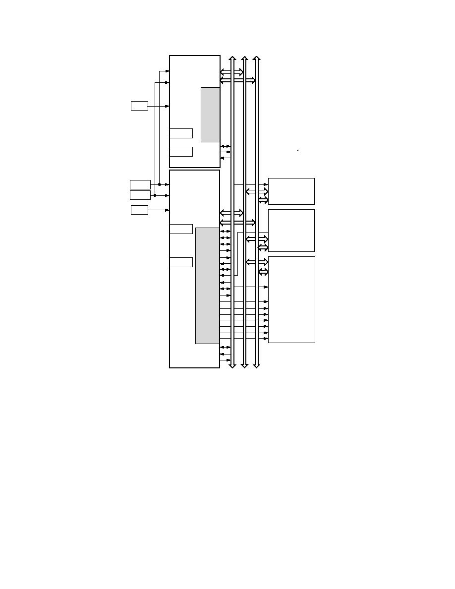
CPA
BR
2
BR
1
CONTROL
ADSP-21065L
#2
ADDR
23-0
DATA
31-0
RESET
CLKIN
RESET
ADSP-21065L
#1
BMS
ADDR
23-0
DATA
31-0
CONTROL
ADDRESS
DATA
CS
ADDR
DATA
BOOT
EPROM
(OPTIONAL)
ADDR
SDRAM
(OPTIONAL)
DATA
ADDR
DATA
HOST
PROCESSOR
(OPTIONAL)
CLOCK
CS
HBR
HBG
REDY
RD
WR
ACK
SBTS
SW
CLKIN
MS
3-0
CPA
CS
RESET
ID
1-0
SPORT0
SPORT1
CS
RAS
CAS
DQM
SDCLK
1-0
SDCKE
SDA10
BR
1
RAS
CAS
DQM
CLK
CKE
A10
SDWE
WE
SPORT0
SPORT1
CONTROL
ID
1-0
01
10
BR
2
Figure 3. Multiprocessing System

REV. B
ADSP-21065L
7
PIN DESCRIPTIONS
ADSP-21065L pin definitions are listed below. Inputs identified as synchronous (S) must meet timing requirements with respect to
CLKIN (or with respect to TCK for TMS, TDI). Inputs identified as asynchronous (A) can be asserted asynchronously to CLKIN
(or to TCK for
TRST).
Unused inputs should be tied or pulled to VDD or GND, except for ADDR
23-0,
DATA
31-0
, FLAG
11-0
,
SW, and inputs that have
internal pull-up or pull-down resistors (
CPA, ACK, DTxX, DRxX, TCLKx, RCLKx, TMS, and TDI)--these pins can be left float-
ing. These pins have a logic-level hold circuit that prevents the input from floating internally.
I = Input
S = Synchronous
P = Power Supply
(O/D) = Open Drain
O = Output
A = Asynchronous
G = Ground
(A/D) = Active Drive
T = Three-state (when
SBTS is asserted, or when the ADSP-2106x is a bus slave)
Pin
Type
Function
ADDR
23-0
I/O/T
External Bus Address. The ADSP-21065L outputs addresses for external memory and pe-
ripherals on these pins. In a multiprocessor system the bus master outputs addresses for read/
writes of the IOP registers of the other ADSP-21065L. The ADSP-21065L inputs addresses
when a host processor or multiprocessing bus master is reading or writing its IOP registers.
DATA
31-0
I/O/T
External Bus Data. The ADSP-21065L inputs and outputs data and instructions on these
pins. The external data bus transfers 32-bit single-precision floating-point data and 32-bit fixed-
point data over bits 31-0. 16-bit short word data is transferred over bits 15-0 of the bus. Pull-up
resistors on unused DATA pins are not necessary.
MS
3-0
I/O/T
Memory Select Lines. These lines are asserted as chip selects for the corresponding banks of
external memory. Internal ADDR
25-24
are decoded into
MS
3-0
. The
MS
3-0
lines are decoded
memory address lines that change at the same time as the other address lines. When no external
memory access is occurring the
MS
3-0
lines are inactive; they are active, however, when a condi-
tional memory access instruction is executed, whether or not the condition is true. Additionally,
an
MS
3-0
line which is mapped to SDRAM may be asserted even when no SDRAM access is
active. In a multiprocessor system, the
MS
3-0
lines are output by the bus master.
RD
I/O/T
Memory Read Strobe. This pin is asserted when the ADSP-21065L reads from external memory
devices or from the IOP register of another ADSP-21065L. External devices (including another
ADSP-21065L) must assert
RD to read from the ADSP-21065L's IOP registers. In a multipro-
cessor system,
RD is output by the bus master and is input by another ADSP-21065L.
WR
I/O/T
Memory Write Strobe. This pin is asserted when the ADSP-21065L writes to external memory
devices or to the IOP register of another ADSP-21065L. External devices must assert
WR to
write to the ADSP-21065L's IOP registers. In a multiprocessor system,
WR is output by the bus
master and is input by the other ADSP-21065L.
SW
I/O/T
Synchronous Write Select. This signal interfaces the ADSP-21065L to synchronous memory
devices (including another ADSP-21065L). The ADSP-21065L asserts
SW to provide an early
indication of an impending write cycle, which can be aborted if
WR is not later asserted (e.g., in
a conditional write instruction). In a multiprocessor system,
SW is output by the bus master and
is input by the other ADSP-21065L to determine if the multiprocessor access is a read or write.
SW is asserted at the same time as the address output.
ACK
I/O/S
Memory Acknowledge. External devices can deassert ACK to add wait states to an external
memory access. ACK is used by I/O devices, memory controllers, or other peripherals to hold
off completion of an external memory access. The ADSP-21065L deasserts ACK as an output
to add wait states to a synchronous access of its IOP registers. In a multiprocessor system, a
slave ADSP-21065L deasserts the bus master's ACK input to add wait state(s) to an access of
its IOP registers. The bus master has a keeper latch on its ACK pin that maintains the input at
the level to which it was last driven.
SBTS
I/S
Suspend Bus Three-State. External devices can assert
SBTS to place the external bus ad-
dress, data, selects, and strobes--but not SDRAM control pins--in a high impedance state for
the following cycle. If the ADSP-21065L attempts to access external memory while
SBTS is
asserted, the processor will halt and the memory access will not finish until
SBTS is deasserted.
SBTS should only be used to recover from host processor/ADSP-21065L deadlock.
IRQ
2-0
I/A
Interrupt Request Lines. May be either edge-triggered or level-sensitive.
FLAG
11-0
I/O/A
Flag Pins. Each is configured via control bits as either an input or an output. As an input, it can
be tested as a condition. As an output, it can be used to signal external peripherals.

REV. B
ADSP-21065L
8
Pin
Type
Function
HBR
I/A
Host Bus Request. Must be asserted by a host processor to request control of the ADSP-
21065L's external bus. When
HBR is asserted in a multiprocessing system, the ADSP-21065L
that is bus master will relinquish the bus and assert
HBG. To relinquish the bus, the ADSP-
21065L places the address, data, select, and strobe lines in a high impedance state. It does,
however, continue to drive the SDRAM control pins.
HBR has priority over all ADSP-21065L
bus requests (
BR
2-1
) in a multiprocessor system.
HBG
I/O
Host Bus Grant. Acknowledges an
HBR bus request, indicating that the host processor may
take control of the external bus.
HBG is asserted by the ADSP-21065L until HBR is released.
In a multiprocessor system,
HBG is output by the ADSP-21065L bus master.
CS
I/A
Chip Select. Asserted by host processor to select the ADSP-21065L.
REDY (O/D)
O
Host Bus Acknowledge. The ADSP-21065L deasserts REDY to add wait states to an asyn-
chronous access of its internal memory or IOP registers by a host. Open drain output (O/D) by
default; can be programmed in ADREDY bit of SYSCON register to be active drive (A/D).
REDY will only be output if the
CS and HBR inputs are asserted.
DMAR
1
I/A
DMA Request 1 (DMA Channel 9).
DMAR
2
I/A
DMA Request 2 (DMA Channel 8).
DMAG
1
O/T
DMA Grant 1 (DMA Channel 9).
DMAG
2
O/T
DMA Grant 2 (DMA Channel 8).
BR
2-1
I/O/S
Multiprocessing Bus Requests. Used by multiprocessing ADSP-21065Ls to arbitrate for bus
mastership. An ADSP-21065L drives its own
BRx line (corresponding to the value of its ID
2-0
inputs) only and monitors all others. In a uniprocessor system, tie both
BRx pins to VDD.
ID
1-0
I
Multiprocessing ID. Determines which multiprocessor bus request (
BR
1
BR
2
) is used by
ADSP-21065L. ID = 01 corresponds to
BR
1
, ID = 10 corresponds to
BR
2
. ID = 00 in single-
processor systems. These lines are a system configuration selection which should be hard-wired
or changed only at reset.
CPA (O/D)
I/O
Core Priority Access. Asserting its
CPA pin allows the core processor of an ADSP-21065L
bus slave to interrupt background DMA transfers and gain access to the external bus.
CPA is an
open drain output that is connected to both ADSP-21065Ls in the system. The
CPA pin has an
internal 5 k
pull-up resistor. If core access priority is not required in a system, leave the CPA
pin unconnected.
DTxX
O
Data Transmit (Serial Ports 0, 1; Channels A, B). Each DTxX pin has a 50 k
internal pull-
up resistor.
DRxX
I
Data Receive (Serial Ports 0, 1; Channels A, B). Each DRxX pin has a 50 k
internal pull-up
resistor.
TCLKx
I/O
Transmit Clock (Serial Ports 0, 1). Each TCLK pin has a 50 k
internal pull-up resistor.
RCLKx
I/O
Receive Clock (Serial Ports 0, 1). Each RCLK pin has a 50 k
internal pull-up resistor.
TFSx
I/O
Transmit Frame Sync (Serial Ports 0, 1).
RFSx
I/O
Receive Frame Sync (Serial Ports 0, 1).
BSEL
I
EPROM Boot Select. When BSEL is high, the ADSP-21065L is configured for booting from
an 8-bit EPROM. When BSEL is low, the BSEL and
BMS inputs determine booting mode. See
BMS for details. This signal is a system configuration selection which should be hard-wired.
REV. B
ADSP-21065L
9
Pin
Type
Function
BMS
I/O/T*
Boot Memory Select. Output: used as chip select for boot EPROM devices (when BSEL = 1).
In a multiprocessor system,
BMS is output by the bus master. Input: When low, indicates that
no booting will occur and that the ADSP-21065L will begin executing instructions from exter-
nal memory. See following table. This input is a system configuration selection which should be
hard-wired.
*Three-statable only in EPROM boot mode (when
BMS is an output).
BSEL
BMS
Booting Mode
1
Output
EPROM (connect
BMS to EPROM chip select).
0
1 (Input)
Host processor (HBW [SYSCON] bit selects host bus width).
0
0 (Input)
No booting. Processor executes from external memory.
CLKIN
I
Clock In. Used in conjunction with XTAL, configures the ADSP-21065L to use either its
internal clock generator or an external clock source. The external crystal should be rated at 1x
frequency.
Connecting the necessary components to CLKIN and XTAL enables the internal clock genera-
tor. The ADSP-21065L's internal clock generator multiplies the 1x clock to generate 2x clock
for its core and SDRAM. It drives 2x clock out on the SDCLKx pins for the SDRAM interface
to use. See also SDCLKx.
Connecting the 1x external clock to CLKIN while leaving XTAL unconnected configures the
ADSP-21065L to use the external clock source. The instruction cycle rate is equal to 2x CLKIN.
CLKIN may not be halted, changed, or operated below the specified frequency.
RESET
I/A
Processor Reset. Resets the ADSP-21065L to a known state and begins execution at the
program memory location specified by the hardware reset vector address. This input must be
asserted at power-up.
TCK
I
Test Clock (JTAG). Provides an asynchronous clock for JTAG boundary scan.
TMS
I/S
Test Mode Select (JTAG). Used to control the test state machine. TMS has a 20 k
internal
pull-up resistor.
TDI
I/S
Test Data Input (JTAG). Provides serial data for the boundary scan logic. TDI has a 20 k
internal pull-up resistor.
TDO
O
Test Data Output (JTAG). Serial scan output of the boundary scan path.
TRST
I/A
Test Reset (JTAG). Resets the test state machine.
TRST must be asserted (pulsed low) after
power-up or held low for proper operation of the ADSP-21065L.
TRST has a 20 k
internal
pull-up resistor.
EMU (O/D)
O
Emulation Status. Must be connected to the ADSP-21065L EZ-ICE target board connector
only.
BMSTR
O
Bus Master Output. In a multiprocessor system, indicates whether the ADSP-21065L is cur-
rent bus master of the shared external bus. The ADSP-21065L drives BMSTR high only while
it is the bus master. In a single-processor system (ID = 00), the processor drives this pin high.
CAS
I/O/T
SDRAM Column Access Strobe. Provides the column address. In conjunction with
RAS,
MSx, SDWE, SDCLKx, and sometimes SDA10, defines the operation for the SDRAM to per-
form.
RAS
I/O/T
SDRAM Row Access Strobe. Provides the row address. In conjunction with
CAS, MSx,
SDWE, SDCLKx, and sometimes SDA10, defines the operation for the SDRAM to perform.
SDWE
I/O/T
SDRAM Write Enable. In conjunction with
CAS, RAS, MSx, SDCLKx, and sometimes
SDA10, defines the operation for the SDRAM to perform.
DQM
O/T
SDRAM Data Mask. In write mode, DQM has a latency of zero and is used to block write
operations.
SDCLK
1-0
I/O/S/T
SDRAM 2x Clock Output. In systems with multiple SDRAM devices connected in parallel,
supports the corresponding increased clock load requirements, eliminating need of off-chip
clock buffers. Either SDCLK
1
or both SDCLKx pins can be three-stated.
SDCKE
I/O/T
SDRAM Clock Enable. Enables and disables the CLK signal. For details, see the data sheet
supplied with your SDRAM device.
REV. B
ADSP-21065L
10
Pin
Type
Function
SDA10
O/T
SDRAM A10 Pin. Enables applications to refresh an SDRAM in parallel with a host access.
XTAL
O
Crystal Oscillator Terminal. Used in conjunction with CLKIN to enable the ADSP-21065L's
internal clock generator or to disable it to use an external clock source. See CLKIN.
PWM_EVENT
1-0
I/O/A
PWM Output/Event Capture.
In PWMOUT mode, is an output pin and functions as a timer
counter. In WIDTH_CNT mode, is an input pin and functions as a pulse counter/event capture.
VDD
P
Power Supply; nominally +3.3 V dc. (33 pins)
GND
G
Power Supply Return. (37 pins)
NC
Do Not Connect. Reserved pins that must be left open and unconnected. (7)
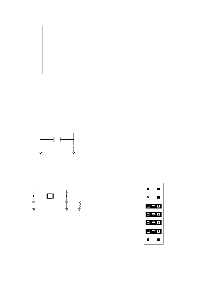
CLOCK SIGNALS
The ADSP-21065L can use an external clock or a crystal. See
CLKIN pin description. You can configure the ADSP-21065L
to use its internal clock generator by connecting the necessary
components to CLKIN and XTAL. You can use either a crystal
operating in the fundamental mode or a crystal operating at an
overtone. Figure 4 shows the component connections used for a
crystal operating in fundamental mode, and Figure 5 shows
the component connections used for a crystal operating at an
overtone.
CLKIN
X1
XTAL
C1
C2
SUGGESTED COMPONENTS FOR 30 MHz OPERATION:
ECLIPTEK EC2SM-33-30.000M (SURFACE MOUNT PACKAGE)
ECLIPTEK EC-33-30.000M (THRU-HOLE PACKAGE)
C1 = 33pF
C2 = 27pF
NOTE: C1 AND C2 ARE SPECIFIC TO CRYSTAL SPECIFIED FOR X1.
CONTACT CRYSTAL MANUFACTURER FOR DETAILS.
Figure 4. 30 MHz Operation (Fundamental Mode Crystal)
CLKIN
XTAL
C1
C2
SUGGESTED COMPONENTS FOR 30MHz OPERATION:
ECLIPTEK EC2SM-T-30.000M (SURFACE MOUNT PACKAGE)
ECLIPTEK ECT-30.000M (THRU-HOLE PACKAGE)
C1 = 18pF
C2 = 27pF
C3 = 75pF
L
1
= 3300nH
R
S
= SEE NOTE.
NOTE: C1, C2, C3, R
S
AND L
1
ARE SPECIFIC TO CRYSTAL SPECIFIED
FOR X1. CONTACT MANUFACTURER FOR DETAILS.
C3
R
S
L1
X1
Figure 5. 30 MHz Operation (3rd Overtone Crystal)
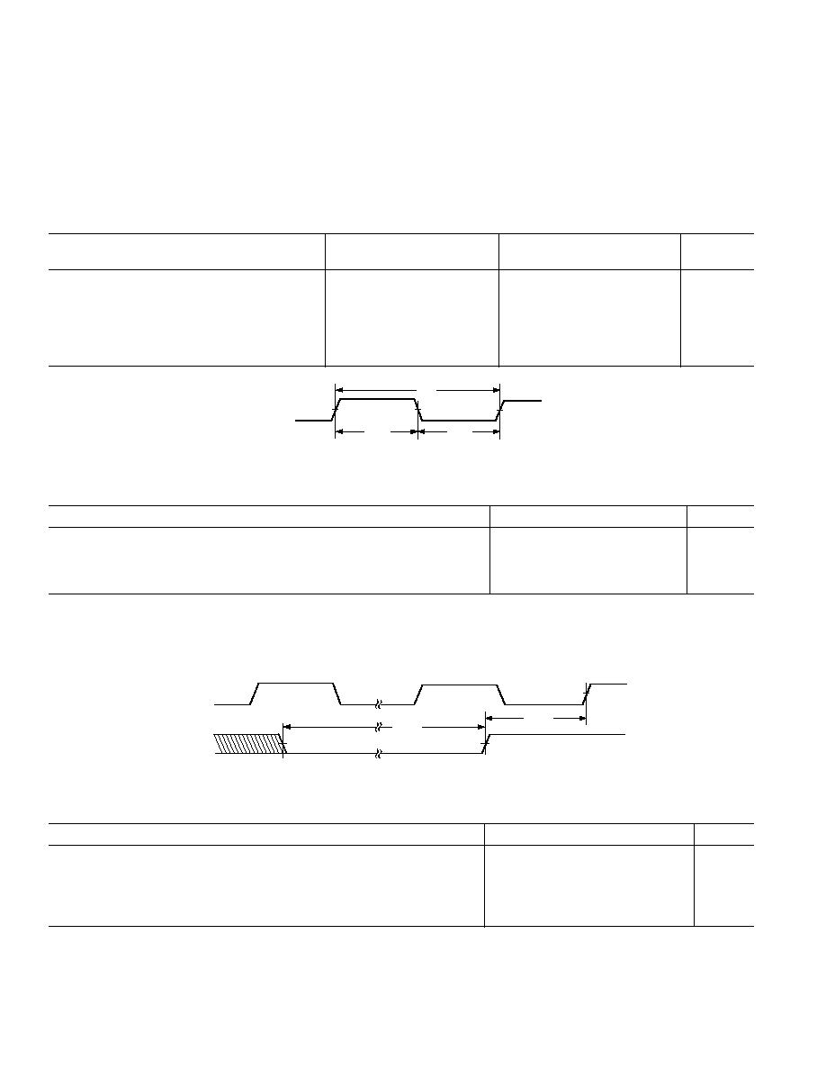
TARGET BOARD CONNECTOR FOR EZ-ICE PROBE
The ADSP-2106x EZ-ICE emulator uses the IEEE 1149.1
JTAG test access port of the ADSP-2106x to monitor and con-
trol the target board processor during emulation. The EZ-ICE
probe requires the ADSP-2106x's CLKIN, TMS, TCK,
TRST,
TDI, TDO,
EMU and GND signals be made accessible on the
target system via a 14-pin connector (a 2 row x 7 pin strip header)
such as that shown in Figure 6. The EZ-ICE probe plugs di-
rectly onto this connector for chip-on-board emulation. You
must add this connector to your target board design if you,
intend to use the ADSP-2106x EZ-ICE.
The total trace length between the EZ-ICE connector and the
furthest device sharing the EZ-ICE JTAG pins should be lim-
ited to 15 inches maximum for guaranteed operation. This
restriction on length must include EZ-ICE JTAG signals, which
are routed to one or more 2106x devices or to a combination of
2106xs and other JTAG devices on the chain.
The 14-pin, 2-row pin strip header is keyed at the Pin 3 loca-
tion--you must remove Pin 3 from the header. The pins must
be 0.025 inch square and at least 0.20 inch in length. Pin spac-
ing should be 0.1
× 0.1 inches. Pin strip headers are available
from vendors such as 3M, McKenzie and Samtec.
TOP VIEW
13
14
11
12
9
10
9
7
8
5
6
3
4
1
2
EMU
CLKIN (OPTIONAL)
TMS
TCK
TRST
TDI
TDO
GND
KEY (NO PIN)
BTMS
BTCK
BTRST
BTDI
GND
Figure 6. Target Board Connector for ADSP-2106x EZ-ICE
(JTAG Header)

REV. B
ADSP-21065L
11
The BTMS, BTCK,
BTRST and BTDI signals are provided so
that the test access port can also be used for board-level testing.
When the connector is not being used for emulation, place
jumpers between the Bxxx pins and the xxx pins. If you are not
going to use the test access port for board testing, tie
BTRST
to GND and tie or pull-up BTCK to V
DD
.
The
TRST pin must
be asserted after power-up (through
BTRST on the connector)
or held low for proper operation of the ADSP-2106x. None of
the Bxxx pins (Pins 5, 7, 9, 11) are connected on the EZ-ICE
probe.
The JTAG signals are terminated on the EZ-ICE probe as follows:
Signal
Termination
TMS
Driven through 22
resistor (16 mA driver)
TCK
Driven at 10 MHz through 22
resistor
(16 mA driver)
TRST*
Driven through 22
resistor (16 mA driver)
(pulled up by on-chip 20 k
resistor)
TDI
Driven by 22
resistor (16 mA driver)
TDO
One TTL load, Split Termination (160/220)
CLKIN
One TTL load, Split Termination (160/220).
(Caution: Do not connect to CLKIN if
internal XTAL oscillator is used.)
EMU
Active Low 4.7 k
pull-up resistor, one TTL
load (open-drain output from ADSP-2106xs)
*
TRST is driven low until the EZ-ICE probe is turned on by the emulator at
software start-up. After software start-up,
TRST is driven high.
Connecting CLKIN to Pin 4 of the EZ-ICE header is optional.
The emulator only uses CLKIN when directed to perform op-
erations such as starting, stopping, and single-stepping two
ADSP-21065Ls in a synchronous manner. If you do not need
these operations to occur synchronously on the two processors,
simply tie Pin 4 of the EZ-ICE header to ground.
For systems which use the internal clock generator and an exter-
nal discrete crystal, do not directly connect the CLKIN pin to
the JTAG probe. This will load the oscillator circuit and possi-
bly cause it to fail to oscillate. Instead the JTAG probe's
CLKIN can be driven by the XTAL pin through a high imped-
ance buffer.
If synchronous multiprocessor operations are needed and CLKIN
is connected, clock skew between multiple ADSP-2106x proces-
sors and the CLKIN pin on the EZ-ICE header must be mini-
mal. If the skew is too large, synchronous operations may be off
by one cycle between processors. For synchronous multiproces-
sor operation TCK, TMS, CLKIN and
EMU should be treated
as critical signals in terms of skew, and should be laid out as
short as possible on your board.
If synchronous multiprocessor operations are not needed (i.e.,
CLKIN is not connected), just use appropriate parallel termina-
tion on TCK and TMS. TDI, TDO,
EMU and TRST are not
critical signals in terms of skew.
For Complete information on the SHARC EZ-ICE, see the
ADSP-21000 Family
JTAG EZ-ICE User's Guide and Reference.

REV. B
12
ADSP-21065LSPECIFICATIONS
RECOMMENDED OPERATING CONDITIONS
Test
C Grade
K Grade
Parameter
Conditions
Min
Max
Min
Max
Units
V
DD
Supply Voltage
3.13
3.60
3.13
3.60
V
T
CASE
Case Operating Temperature
40
+100
0
+85
°C
V
IH
High Level Input Voltage
@ V
DD
= max
2.0
V
DD
+ 0.5
2.0
V
DD
+ 0.5
V
V
IL1
Low Level Input Voltage
1
@ V
DD
= min
0.5
0.8
0.5
0.8
V
V
IL2
Low Level Input Voltage
2
@ V
DD
= min
0.5
0.7
0.5
0.7
V
NOTE
See Environmental Conditions for information on thermal specifications.
ELECTRICAL CHARACTERISTICS
C & K Grades
Parameter
Test Conditions
Min
Max
Units
V
OH
High Level Output Voltage
3
@ V
DD
= min, I
OH
= 2.0 mA
4
2.4
V
V
OL
Low Level Output Voltage
3
@ V
DD
= min, I
OL
= 4.0 mA
4
0.4
V
I
IH
High Level Input Current
5
@ V
DD
= max, V
IN
= V
DD
max
10
µA
I
IL
Low Level Input Current
5
@ V
DD
= max, V
IN
= 0 V
10
µA
I
ILP
Low Level Input Current
6
@ V
DD
= max, V
IN
= 0 V
150
µA
I
OZH
Three-State Leakage Current
7, 8, 9, 10
@ V
DD
= max, V
IN
= V
DD
max
10
µA
I
OZL
Three-State Leakage Current
7
@ V
DD
= max, V
IN
= 0 V
8
µA
I
OZLS
Three-State Leakage Current
8
@ V
DD
= max, V
IN
= 0 V
150
µA
I
OZLA
Three-State Leakage Current
11
@ V
DD
= max, V
IN
= 1.5 V
350
µA
I
OZLAR
Three-State Leakage Current
10
@ V
DD
= max, V
IN
= 0 V
4
mA
I
OZLC
Three-State Leakage Current
9
@ V
DD
= max, V
IN
= 0 V
1.5
mA
C
IN
Input Capacitance
12, 13
f
IN
= 1 MHz, T
CASE
= 25
°C, V
IN
= 2.5 V
8
pF
NOTES
1
Applies to input and bidirectional pins: DATA
31-0
, ADDR
23-0
, BSEL,
RD, WR, SW, ACK, SBTS, IRQ
2-0
, FLAG
11-0
,
HBG, CS, DMAR1, DMAR2, BR
2-1
,
ID
2-0
,
RPBA,
CPA, TFS0, TFS1, RFS0, RFS1, BMS, TMS, TDI, TCK, HBR, DR0A, DR1A, DR0B, DR1B, TCLK0, TCLK1, RCLK0, RCLK1, RESET, TRST,
PWM_EVENT0, PWM_EVENT1,
RAS, CAS, SDWE, SDCKE.
2
Applies to input pin CLKIN.
3
Applies to output and bidirectional pins: DATA
31-0
, ADDR
23-0
, MS
3-0
,
RD, WR, SW, ACK, FLAG
11-0
,
HBG, REDY, DMAG1, DMAG2, BR
2-1
,
CPA, TCLK0,
TCLK1, RCLK0, RCLK1, TFS0, TFS1, RFS0, RFS1, DT0A, DT1A, DT0B, DT1B, XTAL,
BMS, TDO, EMU, BMSTR, PWM_EVENT0, PWM_EVENT1,
RAS, CAS, DQM, SDWE, SDCLK0, SDCLK1, SDCKE, SDA10.
4
See Output Drive Currents for typical drive current capabilities.
5
Applies to input pins: ACK,
SBTS, IRQ
2-0
,
HBR, CS, DMAR1, DMAR2, ID
1-0
, BSEL, CLKIN,
RESET, TCK (Note that ACK is pulled up internally with 2 k
during reset in a multiprocessor system, when ID
1-0
= 01 and another ADSP-21065L is not requesting bus mastership.)
6
Applies to input pins with internal pull-ups: DR0A, DR1A, DR0B, DR1B,
TRST, TMS, TDI.
7
Applies to three-statable pins: DATA
31-0
, ADDR
23-0
,
MS
3-0
,
RD, WR, SW, ACK, FLAG
11-0
, REDY,
HBG, DMAG
1
,
DMAG
2
,
BMS, TDO, RAS, CAS, DQM,
SDWE, SDCLK0, SDCLK1, SDCKE, SDA10 and EMU (Note that ACK is pulled up internally with 2 k
during reset in a multiprocessor system, when ID
1-0
=
01 and another ADSP-21065L is not requesting bus mastership).
8
Applies to three-statable pins with internal pull-ups: DT0A, DT1A, DT0B, DT1B, TCLK0, TCLK1, RCLK0, RCLK1.
9
Applies to
CPA pin.
10
Applies to ACK pin when pulled up.
11
Applies to ACK pin when keeper latch enabled.
12
Guaranteed but not tested.
13
Applies to all signal pins.
Specifications subject to change without notice.
ABSOLUTE MAXIMUM RATINGS*
Supply Voltage . . . . . . . . . . . . . . . . . . . . . . . . 0.3 V to +4.6 V
Input Voltage . . . . . . . . . . . . . . . . . . . . . 0.5 V to V
DD
+ 0.5 V
Output Voltage Swing . . . . . . . . . . . . . . 0.5 V to V
DD
+ 0.5 V
Load Capacitance . . . . . . . . . . . . . . . . . . . . . . . . . . . . . 200 pF
Junction Temperature Under Bias . . . . . . . . . . . . . . . . . 130
°C
Storage Temperature Range . . . . . . . . . . . . . 65
°C to +150°C
Lead Temperature (5 seconds) . . . . . . . . . . . . . . . . . . +280
°C
*Stresses greater than those listed above may cause permanent damage to the device.
These are stress ratings only; functional operation of the device at these or any other
conditions greater than those indicated in the operational sections of this specifica-
tion is not implied. Exposure to absolute maximum rating conditions for extended
periods may affect device reliability.
ESD SENSITIVITY
ESD (electrostatic discharge) sensitive device. Electrostatic charges as high as 4000 V readily
accumulate on the human body and test equipment and can discharge without detection. Although
the ADSP-21065L features proprietary ESD protection circuitry, permanent damage may occur on
devices subjected to high-energy electrostatic discharges. Therefore, proper ESD precautions are
recommended to avoid performance degradation or loss of functionality.
WARNING!
ESD SENSITIVE DEVICE
REV. B
ADSP-21065L
13
POWER DISSIPATION ADSP-21065L
These specifications apply to the internal power portion of V
DD
only. See the Power Dissipation section of this data sheet for calcula-
tion of external supply current and total supply current. For a complete discussion of the code used to measure power dissipation, see
the technical note SHARC Power Dissipation Measurements.
Specifications are based on the following operating scenarios:
Table II. Internal Current Measurements
Peak Activity
High Activity
Operation
(I
DDINPEAK
)
(I
DDINHIGH
)
Low Activity (I
DDINLOW
)
Instruction Type
Multifunction
Multifunction
Single Function
Instruction Fetch
Cache
Internal Memory
Internal Memory
Core Memory Access
2 per Cycle (DM and PM)
1 per Cycle (DM)
None
Internal Memory DMA
1 per Cycle
1 per 2 Cycles
1 per 2 Cycles
To estimate power consumption for a specific application, use the following equation where % is the amount of time your program
spends in that state:
%PEAK
× I
DDINPEAK
+ %HIGH
× I
DDINHIGH
+ %LOW
× I
DDINLOW
+ %IDLE16
× I
DDIDLE16
= POWER CONSUMPTION
Table III. Internal Current Measurement Scenarios
Parameter
Test Conditions
Max
Units
I
DDINPEAK
Supply Current (Internal)
1
t
CK
= 33 ns, V
DD
= max
470
mA
t
CK
= 30 ns, V
DD
= max
510
mA
I
DDINHIGH
Supply Current (Internal)
2
t
CK
= 33 ns, V
DD
= max
275
mA
t
CK
= 30 ns, V
DD
= max
300
mA
I
DDINLOW
Supply Current (Internal)
3
t
CK
= 33 ns, V
DD
= max
240
mA
t
CK
= 30 ns, V
DD
= max
260
mA
I
DDIDLE
Supply Current (IDLE)
4
t
CK
= 33 ns, V
DD
= max
150
mA
t
CK
= 30 ns, V
DD
= max
155
mA
I
DDIDLE16
Supply Current (IDLE16)
5
V
DD
= max
50
mA
NOTES
1
The test program used to measure I
DDINPEAK
represents worst case processor operation and is not sustainable under normal application conditions. Actual internal
power measurements made using typical applications are less than specified.
2
I
DDINHIGH
is a composite average based on a range of high activity code.
3
I
DDINLOW
is a composite average based on a range of low activity code.
4
IDLE denotes ADSP-21065L state during execution of IDLE instruction.
5
IDLE16 denotes ADSP-21065L state during execution of IDLE16 instruction.
TIMING SPECIFICATIONS
General Notes
Two speed grades of the ADSP-21065L are offered, 60 MHz and 66 MHz instruction rates. The specifications shown are based on a
CLKIN frequency of 30 MHz (t
CK
= 33.3 ns). The DT derating allows specifications at other CLKIN frequencies (within the min
max range of the t
CK
specification; see Clock Input below). DT is the difference between the actual CLKIN period and a CLKIN
period of 33.3 ns:
DT = (t
CK
33.3)/32
Use the exact timing information given. Do not attempt to derive parameters from the addition or subtraction of others. While addi-
tion or subtraction would yield meaningful results for an individual device, the values given in this data sheet reflect statistical varia-
tions and worst cases. Consequently, you cannot meaningfully add parameters to derive longer times.
See Figure 27 in Equivalent Device Loading for AC Measurements (Includes All Fixtures) for voltage reference levels.
REV. B
ADSP-21065L
14
Switching Characteristics specify how the processor changes its signals. You have no control over this timing--circuitry external to the
processor must be designed for compatibility with these signal characteristics. Switching characteristics tell you what the processor
will do in a given circumstance. You can also use switching characteristics to ensure that any timing requirement of a device con-
nected to the processor (such as memory) is satisfied.
Timing Requirements apply to signals that are controlled by circuitry external to the processor, such as the data input for a read opera-
tion. Timing requirements guarantee that the processor operates correctly with other devices.
(O/D) = Open Drain
(A/D) = Active Drive
66 MHz
60 MHz
Parameter
Min
Max
Min
Max
Units
Clock Input
Timing Requirements:
t
CK
CLKIN Period
30.00
100
33.33
100
ns
t
CKL
CLKIN Width Low
7.0
7.0
ns
t
CKH
CLKIN Width High
5.0
5.0
ns
t
CKRF
CLKIN Rise/Fall (0.4 V2.0 V)
3.0
3.0
ns
CLKIN
t
CKH
t
CK
t
CKL
Figure 7. Clock Input
Parameter
Min
Max
Units
Reset
Timing Requirements:
t
WRST
RESET Pulsewidth Low
1
2 t
CK
ns
t
SRST
RESET Setup Before CLKIN High
2
23.5 + 24 DT t
CK
ns
NOTES
1
Applies after the power-up sequence is complete. At power-up, the processor's internal phase-locked loop requires no more than 3000 CLKIN cycles while
RESET is
low, assuming stable V
DD
and CLKIN (not including start-up time of external clock oscillator).
2
Only required if multiple ADSP-2106xs must come out of reset synchronous to CLKIN with program counters (PC) equal (i.e., for a SIMD system). Not required
for multiple ADSP-2106xs communicating over the shared bus (through the external port), because the bus arbitration logic synchronizes itself automatically after
reset.
CLKIN
RESET
t
WRST
t
SRST
Figure 8. Reset
Parameter
Min
Max
Units
Interrupts
Timing Requirements:
t
SIR
IRQ2-0 Setup Before CLKIN High or Low
1
11.0 + 12 DT
ns
t
HIR
IRQ2-0 Hold Before CLKIN High or Low
1
0.0 + 12 DT
ns
t
IPW
IRQ2-0 Pulsewidth
2
2.0 + t
CK
/2
ns
NOTES
1
Only required for
IRQx recognition in the following cycle.
2
Applies only if t
SIR
and t
HIR
requirements are not met.
REV. B
ADSP-21065L
15
CLKIN
IRQ2-0
t
IPW
t
SIR
t
HIR
Figure 9. Interrupts
Parameter
Min
Max
Units
Timer
Timing Requirements:
t
STI
Timer Setup Before SDCLK High
0.0
ns
t
HTI
Timer Hold After SDCLK High
6.0
ns
Switching Characteristics:
t
DTEX
Timer Delay After SDCLK High
1.0
ns
t
HTEX
Timer Hold After SDCLK High
5.0
ns
Parameter
Min
Max
Units
Flags
Timing Requirements:
t
SFI
FLAG
11-0
IN Setup Before SDCLK High
1
2.0
ns
t
HFI
FLAG
11-0
IN Hold After SDCLK High
1
6.0
ns
Switching Characteristics:
t
DFO
FLAG
11-0
OUT Delay After SDCLK High
1.0
ns
t
HFO
FLAG
11-0
OUT Hold After SDCLK High
4.0
ns
t
DFOE
SDCLK High to FLAG
11-0
OUT Enable
4.0
ns
t
DFOD
SDCLK High to FLAG
11-0
OUT Disable
1.75
ns
NOTE
1
Flag inputs meeting these setup and hold times will affect conditional instructions in the following instruction cycle.
SDCLK
FLAG
110
OUT
FLAG OUTPUT
t
DFO
t
HFO
t
DFO
t
DFOD
t
DFOE
SDCLK
t
SFI
t
HFI
FLAG
110
IN
Figure 10. Flags
REV. B
ADSP-21065L
16
Memory Read--Bus Master
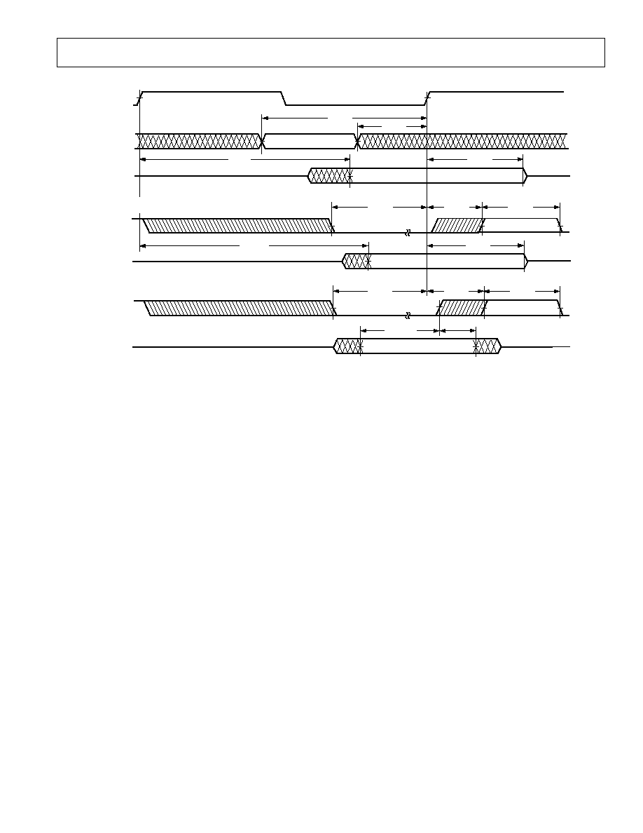
Use these specifications for asynchronous interfacing to memories (and memory-mapped peripherals) without reference to CLKIN.
These specifications apply when the ADSP-21065L is the bus master when accessing external memory space. These switching char-
acteristics also apply for bus master synchronous read/write timing (see Synchronous Read/Write--Bus Master below). If these tim-
ing requirements are met, the synchronous read/write timing can be ignored (and vice versa). An exception to this is the ACK pin
timing requirements as described in the note below.
Parameter
Min
Max
Units
Timing Requirements:
t
DAD
Address, Selects Delay to Data Valid
1, 2
28.0 + 32 DT + W
ns
t
DRLD
RD Low to Data Valid
1
24.0 + 26 DT + W
ns
t
HDA
Data Hold from Address Selects
3
0.0
ns
t
HDRH
Data Hold from
RD High
3
0.0
ns
t
DAAK
ACK Delay from Address, Selects
2, 3
24.0 + 30 DT + W
ns
t
DSAK
ACK Delay from
RD Low
3
19.5 + 24 DT + W
ns
Switching Characteristics:
t
DRHA
Address, Selects Hold After
RD High
1.0 + H
ns
t
DARL
Address, Selects to
RD Low
2
3.0 + 6 DT
ns
t
RW
RD Pulsewidth
25.0 + 26 DT + W
ns
t
RWR
RD High to WR, RD Low
4.5 + 6 DT + HI
ns
t
RDGL
RD High to DMAGx Low
11.0 +12 DT + HI
ns
W = (number of wait states specified in WAIT register)
× t
CK
.
HI = t
CK
(if an address hold cycle or bus idle cycle occurs, as specified in WAIT register; otherwise HI = 0).
H = t
CK
(if an address hold cycle occurs as specified in WAIT register; otherwise H = 0).
NOTES
1
Data Delay/Setup: User must meet t
DAD
or to t
DRLD
or synchronous specification t
SSDATI
.
2
The falling edge of
MSx, SW, BMS, are referenced.
3
ACK is not sampled on external memory accesses that use the Internal wait state mode. For the first CLKIN cycle of a new external memory access, ACK must be
valid by t
DAAK
or t
DSAK
or synchronous specification t
SACKC
for wait state modes External, Either, or Both (Both, if the internal wait state is zero). For the second and
subsequent cycles of a wait stated external memory access, synchronous specifications t
SACKC
and t
HACKC
must be met for wait state modes External, Either, or Both
(Both, after internal wait states have completed).
WR
ACK
DATA
RD
ADDRESS
MSx , SW
BMS
t
DARL
t
RW
t
DAAK
t
RWR
t
DRHA
t
DSAK
DMAG
t
HDRH
t
RDGL
t
DRLD
t
DAD
t
HDA
Figure 11. Memory Read--Bus Master
REV. B
ADSP-21065L
17
Memory Write--Bus Master
Use these specifications for asynchronous interfacing to memories (and memory-mapped peripherals) without reference to CLKIN.
These specifications apply when the ADSP-21065L is the bus master when accessing external memory space. These switching char-
acteristics also apply for bus master synchronous read/write timing (see Synchronous Read/Write--Bus Master below). If these tim-
ing requirements are met, the synchronous read/write timing can be ignored (and vice versa). An exception to this is the ACK pin
timing requirements as described in the note below.
Parameter
Min
Max
Units
Timing Requirements:
t
DAAK
ACK Delay from Address
1, 2
24.0 + 30 DT + W
ns
t
DSAK
ACK Delay from
WR Low
1
19.5 + 24 DT + W
ns
Switching Characteristics:
t
DAWH
Address, Selects to
WR Deasserted
2
29.0 + 31 DT + W
ns
t
DAWL
Address, Selects to
WR Low
2
3.5 + 6 DT
ns
t
WW
WR Pulsewidth
24.5 + 25 DT + W
ns
t
DDWH
Data Setup Before
WR High
15.5 + 19 DT + W
ns
t
DWHA
Address Hold After
WR Deasserted
0.0 + 1 DT + H
ns
t
DATRWH
Data Disable After
WR Deasserted
3
1.0 + 1 DT + H
4.0 + 1 DT + H
ns
t
WWR
WR High to WR, RD Low
4.5 + 7 DT + H
ns
t
WRDGL
WR High to DMAGx Low
11.0 + 13 DT + H
ns
t
DDWR
Data Disable Before
WR or RD Low
3.5 + 6 DT + I
ns
t
WDE
WR Low to Data Enabled
4.5 + 6 DT
ns
W = (number of wait states specified in WAIT register)
× t
CK
.
H = t
CK
(if an address hold cycle occurs, as specified in WAIT register; otherwise H = 0).
I = t
CK
(if a bus idle cycle occurs, as specified in WAIT register; otherwise I = 0).
NOTES
1
ACK is not sampled on external memory accesses that use the Internal wait state mode. For the first CLKIN cycle of a new external memory access, ACK must be
valid by t
DAAK
or t
DSAK
or synchronous specification t
SACKC
for wait state modes External, Either, or Both (Both, if the internal wait state is zero). For the second and
subsequent cycles of a wait stated external memory access, synchronous specifications t
SACKC
and t
HACKC
must be met for wait state modes External, Either, or Both
(Both, after internal wait states have completed).
2
The falling edge of
MSx, SW, and BMS is referenced.
3
See System Hold Time Calculation under Test Conditions for calculation of hold times given capacitive and dc loads.
RD
ACK
DATA
WR
ADDRESS
MSx , SW
BMS
t
DAWL
t
WW
t
DAAK
t
WWR
t
WDE
t
DDWR
t
DWHA
t
DDWH
t
DAWH
t
DSAK
DMAG
t
DATRWH
t
WRDGL
Figure 12. Memory Write--Bus Master

REV. B
ADSP-21065L
18
Synchronous Read/Write--Bus Master
Use these specifications for interfacing to external memory systems that require CLKIN-relative timing or for accessing a slave
ADSP-21065L (in multiprocessor memory space). These synchronous switching characteristics are also valid during asynchronous
memory reads and writes (see Memory Read--Bus Master and Memory Write--Bus Master).
When accessing a slave ADSP-21065L, these switching characteristics must meet the slave's timing requirements for synchronous
read/writes (see Synchronous Read/Write--Bus Slave). The slave ADSP-21065L must also meet these (bus master) timing require-
ments for data and acknowledge setup and hold times.
Parameter
Min
Max
Units
Timing Requirements:
t
SSDATI
Data Setup Before CLKIN
0.25 + 2 DT
ns
t
HSDATI
Data Hold After CLKIN
4.0 2 DT
ns
t
DAAK
ACK Delay After Address,
MSx, SW, BMS
1, 2
24.0 + 30 DT + W
ns
t
SACKC
ACK Setup Before CLKIN
1
2.75 + 4 DT
ns
t
HACK
ACK Hold After CLKIN
2.0 4 DT
ns
Switching Characteristics:
t
DADRO
Address,
MSx, BMS, SW Delay After CLKIN
1
7.0 2 DT
ns
t
HADRO
Address,
MSx, BMS, SW Hold After CLKIN
0.5 2 DT
ns
t
DRDO
RD High Delay After CLKIN
0.5 2 DT
6.0 2 DT
ns
t
DWRO
WR High Delay After CLKIN
0.0 3 DT
6.0 3 DT
ns
t
DRWL
RD/WR Low Delay After CLKIN
7.5 + 4 DT
11.75 + 4 DT
ns
t
DDATO
Data Delay After CLKIN
22.0 + 10 DT
ns
t
DATTR
Data Disable After CLKIN
3
1.0 2 DT
7.0 2 DT
ns
t
DBM
BMSTR Delay After CLKIN
3.0
ns
t
HBM
BMSTR Hold After CLKIN
4.0
ns
W = (number of wait states specified in WAIT register)
× t
CK
.
NOTES
1
Data Hold: User must meet t
HDA
or t
HDRH
or synchronous specification t
HDATI
. See system hold time calculation under test conditions for the calculation of hold
times given capacitive and dc loads.
2
ACK is not sampled on external memory accesses that use the Internal wait state mode. For the first CLKIN cycle of a new external memory access, ACK must be
valid by t
DAAK
or t
DSAK
or synchronous specification t
SACKC
for wait state modes External, Either, or Both (Both, if the internal wait state is zero). For the second and
subsequent cycles of a wait stated external memory access, synchronous specifications t
SACKC
and t
HACKC
must be met for wait state modes External, Either, or Both
(Both, after internal wait states have completed).
3
See System Hold Time Calculation under Test Conditions for calculation of hold times given capacitive and dc loads.
REV. B
ADSP-21065L
19
CLKIN
ADDRESS
SW
ACK
(IN)
RD
DATA
(OUT)
WR
t
HADRO
t
DAAK
t
DRWL
t
SACKC
t
HACKC
t
HSDATI
t
SSDATI
t
DRDO
t
DWRO
t
DATTR
t
DDATO
t
DRWL
DATA
(IN)
t
DADRO
WRITE CYCLE
READ CYCLE
Figure 13. Synchronous Read/Write--Bus Master
REV. B
ADSP-21065L
20
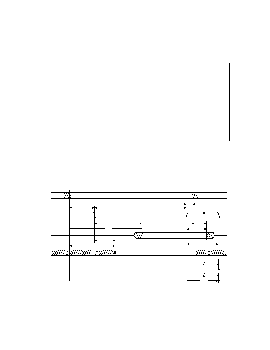
Synchronous Read/Write--Bus Slave
Use these specifications for ADSP-21065L bus master accesses of a slave's IOP registers or internal memory (in multiprocessor
memory space). The bus master must meet these (bus slave) timing requirements.
Parameter
Min
Max
Units
Timing Requirements:
t
SADRI
Address,
SW Setup Before CLKIN
24.5 + 25 DT
ns
t
HADRI
Address,
SW Hold Before CLKIN
4.0 + 8 DT
ns
t
SRWLI
RD/WR Low Setup Before CLKIN
1
21.0 + 21 DT
ns
t
HRWLI
RD/WR Low Hold After CLKIN
2.50 5 DT
7.5 + 7 DT
ns
t
RWHPI
RD/WR Pulse High
2.5
ns
t
SDATWH
Data Setup Before
WR High
4.5
ns
t
HDATWH
Data Hold After
WR High
0.0
ns
Switching Characteristics:
t
SDDATO
Data Delay After CLKIN
31.75 + 21 DT
ns
t
DATTR
Data Disable After CLKIN
2
1.0 2 DT
7.0 2 DT
ns
t
DACK
ACK Delay After CLKIN
29.5 + 20 DT
ns
t
ACKTR
ACK Disable After CLKIN
2
1.0 2 DT
6.0 2 DT
ns
NOTES
1
t
SRWLI
is specified when Multiprocessor Memory Space Wait State (MMSWS bit in WAIT register) is disabled; when MMSWS is enabled, t
SRWLI
(min) = 17.5 + 18 DT.
2
See System Hold Time Calculation under Test Conditions for calculation of hold times given capacitive and dc loads.
For two ADSP-21065Ls to communicate synchronously as master and slave, certain master and slave specification combinations
must be satisfied. Do not compare specification values directly to calculate master/slave clock skew margins for those specifications
listed below. The following table shows the appropriate clock skew margin.
Table IV. Bus Master to Slave Skew Margins
Master Specification
Slave Specification
Skew Margin
t
SSDATI
t
SDDATO
t
CK
= 33.3 ns + 2.25 ns
t
CK
= 30.0 ns
+ 1.50 ns
t
SACKC
t
DACK
t
CK
= 33.3 ns
+ 3.00 ns
t
CK
= 30.0 ns
+ 2.25 ns
t
DADRO
t
SADRI
t
CK
= 33.3 ns
N/A
t
CK
= 30.0 ns
+ 2.75 ns
t
DRWL
(Max)
t
SRWLI
t
CK
= 33.3 ns
+ 1.50 ns
t
CK
= 30.0 ns
+ 1.25 ns
t
DRDO
(Max)
t
HRWLI
(Max)
t
CK
= 33.3 ns
N/A
t
CK
= 30.0 ns
3.00 ns
t
DWRO
(Max)
t
HRWLI
(Max)
t
CK
= 33.3 ns
N/A
t
CK
= 30.0 ns
3.75 ns
REV. B
ADSP-21065L
21
CLKIN
ADDRESS
SW
ACK
RD
DATA
(OUT)
WR
WRITE ACCESS
t
SADRI
t
HADRI
t
DACK
t
ACKTR
t
RWHPI
t
HRWLI
t
SRWLI
t
SDDATO
t
DATTR
t
SRWLI
t
HRWLI
t
RWHPI
t
HDATWH
t
SDATWH
DATA
(IN)
READ ACCESS
Figure 14. Synchronous Read/Write--Bus Slave

REV. B
ADSP-21065L
22
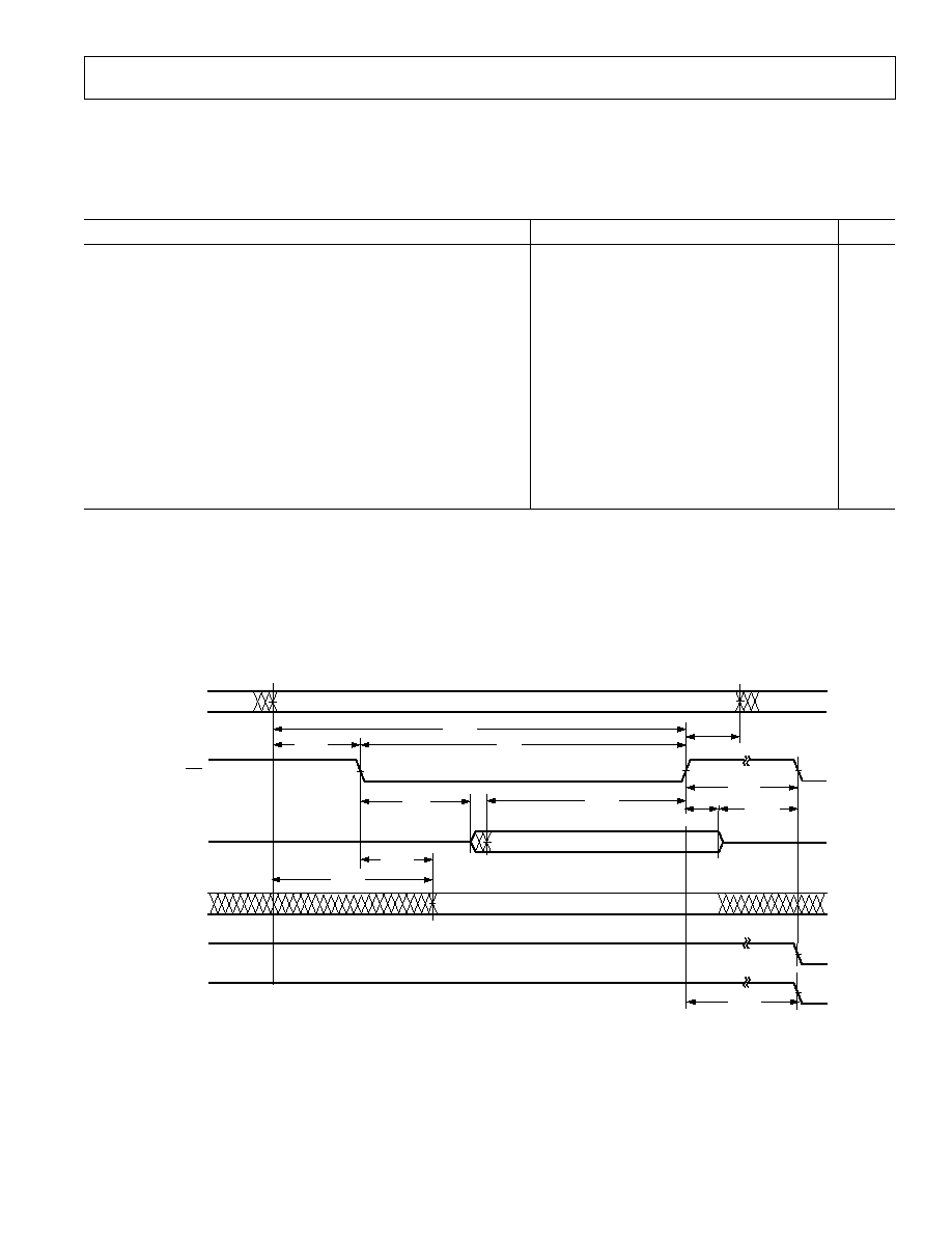
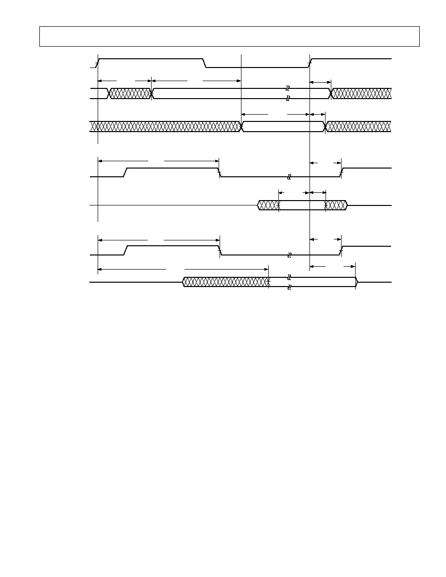
Multiprocessor Bus Request and Host Bus Request
Use these specifications for passing of bus mastership between multiprocessing ADSP-21065Ls (
BRx) or a host processor (HBR,
HBG).
Parameter
Min
Max
Units
Timing Requirements:
t
HBGRCSV
HBG Low to RD/WR/CS Valid
1
20.0 + 36 DT
ns
t
SHBRI
HBR Setup Before CLKIN
2
12.0 + 12 DT
ns
t
HHBRI
HBR Hold Before CLKIN
2
6.0 + 12 DT
ns
t
SHBGI
HBG Setup Before CLKIN
6.0 + 8 DT
ns
t
HHBGI
HBG Hold Before CLKIN High
1.0 + 8 DT
ns
t
SBRI
BRx, CPA Setup Before CLKIN
3
7.0 + 8 DT
ns
t
HBRI
BRx, CPA Hold Before CLKIN High
1.0 + 8 DT
ns
Switching Characteristics:
t
DHBGO
HBG Delay After CLKIN
8.0 2 DT
ns
t
HHBGO
HBG Hold After CLKIN
1.0 2 DT
ns
t
DBRO
BRx Delay After CLKIN
7.0 2 DT
ns
t
HBRO
BRx Hold After CLKIN
1.0 2 DT
ns
t
DCPAO
CPA Low Delay After CLKIN
11.5 2 DT
ns
t
TRCPA
CPA Disable After CLKIN
1.0 2 DT
5.5 2 DT
ns
t
DRDYCS
REDY (O/D) or (A/D) Low from
CS and HBR Low
4
13.0
ns
t
TRDYHG
REDY (O/D) Disable or REDY (A/D) High from
HBG
4
44.0 + 43 DT
ns
t
ARDYTR
REDY (A/D) Disable from
CS or HBR High
4
10.0
ns
NOTES
1
For first asynchronous access after
HBR and CS asserted, ADDR
23-0
must be a nonMMS value 1/2 t
CK
before
RD or WR goes low or by t
HBGRCSV
after
HBG goes
low. This is easily accomplished by driving an upper address signal high when
HBG is asserted. See the Host Processor Control of the ADSP-21065L section of the
ADSP-21065L SHARC User's Manual, Second Edition.
2
Only required for recognition in the current cycle.
3
CPA assertion must meet the setup to CLKIN; deassertion does not need to meet the setup to CLKIN.
4
(O/D) = open drain, (A/D) = active drive.
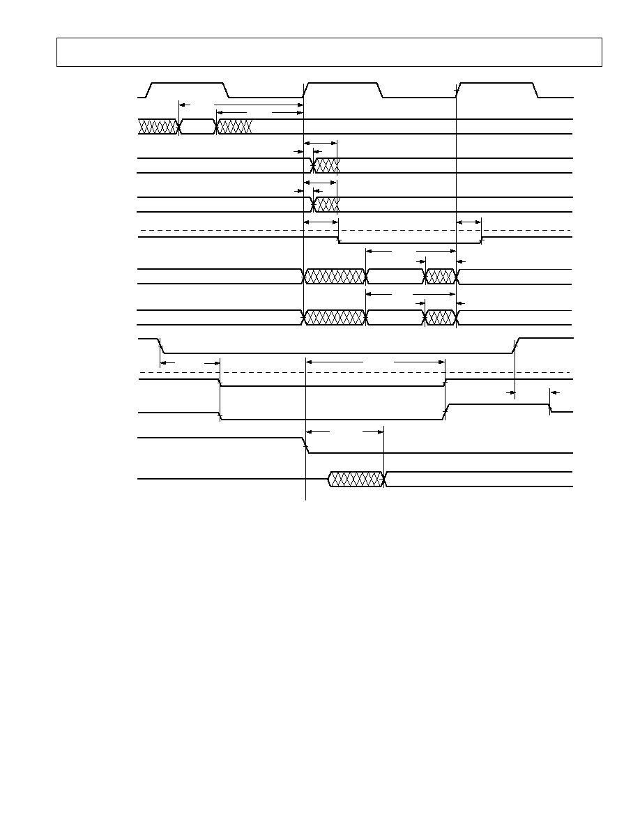
REV. B
ADSP-21065L
23
CLKIN
HBR
HBG
(OUT)
BRx
(OUT)
HBG (IN)
BRx (IN)
HBR
REDY (O/D)
CS
HBG (OUT)
t
DRDYCS
t
HBGRCSV
t
TRDYHG
REDY (A/D)
t
ARDYTR
RD
WR
CS
t
SHBRI
t
HHBRI
t
HHBGO
t
DHBGO
t
HBRO
t
DBRO
t
DCPAO
t
TRCPA
t
SHBGI
t
SBRI
CPA (OUT)
(O/D)
CPA (IN) (O/D)
t
HHBGI
t
HBRI
O/D = OPEN DRAIN, A/D = ACTIVE DRIVE
Figure 15. Multiprocessor Bus Request and Host Bus Request

REV. B
ADSP-21065L
24
Asynchronous Read/Write--Host to ADSP-21065L
Use these specifications for asynchronous host processor accesses of an ADSP-21065L, after the host has asserted
CS and HBR
(low). After the ADSP-21065L returns
HBG, the host can drive the RD and WR pins to access the ADSP-21065L's IOP registers.
HBR and HBG are assumed low for this timing. Writes can occur at a minimum interval of (1/2) t
CK
.
Parameter
Min
Max
Units
Read Cycle
Timing Requirements:
t
SADRDL
Address Setup
/
CS Low Before RD Low*
0.0
ns
t
HADRDH
Address Hold/
CS Hold Low After RD High
0.0
ns
t
WRWH
RD/WR High Width
6.0
ns
t
DRDHRDY
RD High Delay After REDY (O/D) Disable
0.0
ns
t
DRDHRDY
RD High Delay After REDY (A/D) Disable
0.0
ns
Switching Characteristics:
t
SDATRDY
Data Valid Before REDY Disable from Low
1.5
ns
t
DRDYRDL
REDY (O/D) or (A/D) Low Delay After
RD Low
13.5
ns
t
RDYPRD
REDY (O/D) or (A/D) Low Pulsewidth for Read
28.0 + DT
ns
t
HDARWH
Data Disable After
RD High
2.0
10.0
ns
Write Cycle
Timing Requirements:
t
SCSWRL
CS Low Setup Before WR Low
0.0
ns
t
HCSWRH
CS Low Hold After WR High
0.0
ns
t
SADWRH
Address Setup Before
WR High
5.0
ns
t
HADWRH
Address Hold After
WR High
2.0
ns
t
WWRL
WR Low Width
7.0
ns
t
WRWH
RD/WR High Width
6.0
ns
t
DWRHRDY
WR High Delay After REDY (O/D) or (A/D) Disable
0.0
ns
t
SDATWH
Data Setup Before
WR High
5.0
ns
t
HDATWH
Data Hold After
WR High
1.0
ns
Switching Characteristics:
t
DRDYWRL
REDY (O/D) or (A/D) Low Delay After
WR/CS Low
13.5
ns
t
RDYPWR
REDY (O/D) or (A/D) Low Pulsewidth for Write
7.75
ns
NOTE
*Not required if
RD and address are valid t
HBGRCSV
after
HBG goes low. For first access after HBR asserted, ADDR23-0 must be a nonMMS value 1/2 t
CLK
before
RD
or
WR goes low or by t
HBGRCSV
after
HBG goes low. This is easily accomplished by driving an upper address signal high when HBG is asserted. See Host Interface, in
the ADSP-21065L SHARC User's Manual, Second Edition.
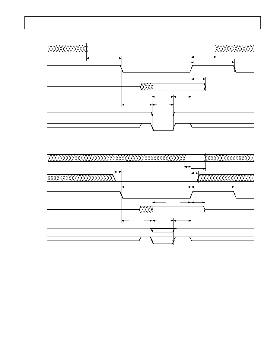
REV. B
ADSP-21065L
25
t
SADRDL
REDY (O/D)
RD
t
DRDYRDL
t
WRWH
t
HADRDH
t
HDARWH
t
RDYPRD
t
DRDHRDY
t
SDATRDY
READ CYCLE
ADDRESS/
CS
DATA (OUT)
REDY (A/D)
O/D = OPEN DRAIN, A/D = ACTIVE DRIVE
t
SDATWH
t
HDATWH
t
WWRL
REDY (O/D)
WR
t
DRDYWRL
t
WRWH
t
HADWRH
t
RDYPWR
t
DWRHRDY
WRITE CYCLE
t
SADWRH
DATA (IN)
ADDRESS
REDY (A/D)
t
SCSWRL
CS
t
HCSWRH
Figure 16. Asynchronous Read/Write--Host to ADSP-21065L

REV. B
ADSP-21065L
26
Three-State Timing--Bus Master, Bus Slave,
HBR, SBTS
These specifications show how the memory interface is disabled (stops driving) or enabled (resumes driving) relative to CLKIN and
the
SBTS pin. This timing is applicable to bus master transition cycles (BTC) and host transition cycles (HTC) as well as the SBTS
pin.
Parameter
Min
Max
Units
Timing Requirements:
t
STSCK
SBTS Setup Before CLKIN
7.0 + 8 DT
ns
t
HTSCK
SBTS Hold Before CLKIN
1.0 + 8 DT
ns
Switching Characteristics:
t
MIENA
Address/Select Enable
After
CLKIN
1.0 2 DT
ns
t
MIENS
Strobes Enable After CLKIN
1
0.5 2 DT
ns
t
MIENHG
HBG Enable After CLKIN
2.0 2 DT
ns
t
MITRA
Address/Select Disable After CLKIN
3.0 4 DT
ns
t
MITRS
Strobes Disable After CLKIN
1
4.0 4 DT
ns
t
MITRHG
HBG Disable After CLKIN
5.5 4 DT
ns
t
DATEN
Data Enable After CLKIN
2
10.0 + 5 DT
ns
t
DATTR
Data Disable After CLKIN
2
1.0 2 DT
7.0 2 DT
ns
t
ACKEN
ACK Enable After CLKIN
2
7.5 + 4 DT
ns
t
ACKTR
ACK Disable After CLKIN
2
1.0 2 DT
6.0 2 DT
ns
t
MTRHBG
Memory Interface Disable Before
HBG Low
3
2.0 + 2 DT
ns
t
MENHBG
Memory Interface Enable After
HBG High
3
15.75 + DT
ns
NOTES
1
Strobes =
RD, WR, SW, DMAG.
2
In addition to bus master transition cycles, these specs also apply to bus master and bus slave synchronous read/write.
3
Memory Interface = Address,
RD, WR, MSx, SW, DMAGx, BMS (in EPROM boot mode).
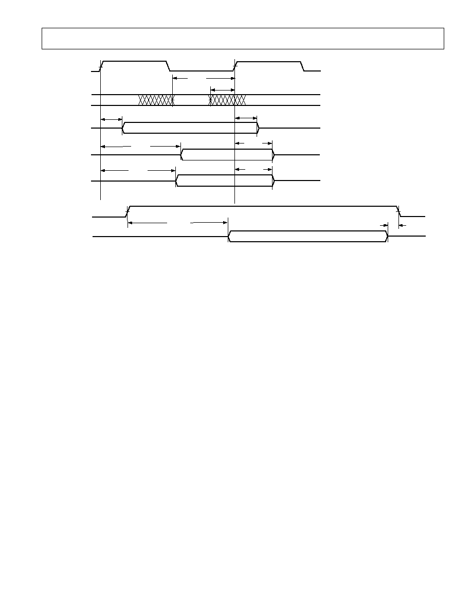
REV. B
ADSP-21065L
27
CLKIN
SBTS
ACK
MEMORY
INTERFACE
t
MENHBG
t
MTRHBG
HBG
MEMORY INTERFACE = ADDRESS,
RD, WR, MSx, SW, DMAGx. BMS (IN EPROM BOOT MODE)
t
MITRA,
t
MITRS,
t
MITRHG
t
STSCK
t
HTSCK
t
DATTR
t
DATEN
t
ACKTR
t
ACKEN
DATA
MEMORY
INTERFACE
t
MIENA,
t
MIENS,
t
MIENHG
Figure 17. Three-State Timing

REV. B
ADSP-21065L
28
DMA Handshake
These specifications describe the three DMA handshake modes. In all three modes DMAR is used to initiate transfers. For hand-
shake mode,
DMAG controls the latching or enabling of data externally. For external handshake mode, the data transfer is controlled
by the ADDR
23-0
,
RD, WR, SW, MS
3-0
, ACK, and
DMAG signals. Extern mode cannot be used for transfers with SDRAM. For
Paced Master mode, the data transfer is controlled by ADDR
23-0
,
RD, WR, MS
3-0
, and ACK (not
DMAG). For Paced Master mode,
the Memory Read-Bus Master, Memory Write-Bus Master, and Synchronous Read/Write-Bus Master timing specifications for
ADDR
23-0
,
RD, WR, MS
3-0
,
SW, DATA
31-0
, and ACK also apply.
Parameter
Min
Max
Units
Timing Requirements:
t
SDRLC
DMARx Low Setup Before CLKIN
1
5.0
ns
t
SDRHC
DMARx High Setup Before CLKIN
1
5.0
ns
t
WDR
DMARx Width Low (Nonsynchronous)
6.0
ns
t
SDATDGL
Data Setup After
DMAGx Low
2
15.0 + 20 DT
ns
t
HDATIDG
Data Hold After
DMAGx High
0.0
ns
t
DATDRH
Data Valid After
DMARx High
2
25.0 + 14 DT
ns
t
DMARLL
DMARx Low Edge to Low Edge
18.0 + 14 DT
ns
t
DMARH
DMARx Width High
6.0
ns
Switching Characteristics:
t
DDGL
DMAGx Low Delay After CLKIN
14.0 + 10 DT
20.0 + 10 DT
ns
t
WDGH
DMAGx High Width
10.0 + 12 DT + HI
ns
t
WDGL
DMAGx Low Width
16.0 + 20 DT
ns
t
HDGC
DMAGx High Delay After
CLKIN
0.0 2 DT
6.0 2 DT
ns
t
DADGH
Address Select Valid to
DMAGx High
28.0 + 16 DT
ns
t
DDGHA
Address Select Hold After
DMAGx High
1.0
ns
t
VDATDGH
Data Valid Before
DMAGx High
3
16.0 + 20 DT
ns
t
DATRDGH
Data Disable After
DMAGx High
4
0.0
4.0
ns
t
DGWRL
WR Low Before DMAGx Low
5.0 + 6 DT
8.0 + 6 DT
ns
t
DGWRH
DMAGx Low Before WR High
18.0 + 19 DT + W
ns
t
DGWRR
WR High Before DMAGx High
0.75 + 1 DT
3.0 + 1 DT
ns
t
DGRDL
RD Low Before DMAGx Low
5.0
8.0
ns
t
DRDGH
RD Low Before DMAGx High
24.0 + 26 DT + W
ns
t
DGRDR
RD High Before DMAGx High
0.0
2.0
ns
t
DGWR
DMAGx High to WR, RD Low
5.0 + 6 DT + HI
ns
W = (number of wait states specified in WAIT register)
× t
CK
.
HI = t
CK
(if an address hold cycle or bus idle cycle occurs, as specified in WAIT register; otherwise HI = 0).
NOTES
1
Only required for recognition in the current cycle.
2
t
SDATDGL
is the data setup requirement if
DMARx is not being used to hold off completion of a write. Otherwise, if DMARx low holds off completion of the write, the
data can be driven t
DATDRH
after
DMARx is brought high.
3
t
VDATDGH
is valid if
DMARx is not being used to hold off completion of a read. If DMARx is used to prolong the read, then t
VDATDGH
= 8 + 9 DT + (n
× t
CK
) where n
equals the number of extra cycles that the access is prolonged.
4
See System Hold Time Calculation under Test Conditions for calculation of hold times given capacitive and dc loads.
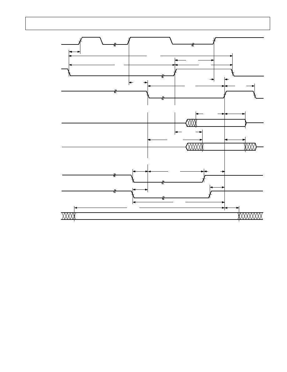
REV. B
ADSP-21065L
29
CLKIN
t
SDRLC
DMARx
DATA (FROM
ADSP-2106x TO
EXTERNAL DEVICE)
DATA (FROM
EXTERNAL DEVICE
TO ADSP-2106x)
RD
(EXTERNAL
MEMORY TO
EXTERNAL DEVICE)
WR
(EXTERNAL DEVICE
TO EXTERNAL
MEMORY)
t
WDR
t
SDRHC
t
DMARH
t
DMARLL
t
HDGC
t
WDGH
t
DDGL
t
WDGL
DMAGx
t
VDATDGH
t
DATDRH
t
DATRDGH
t
HDATIDG
t
DGWRL
t
DGWRH
t
DGWRR
t
DGRDL
t
DRDGH
t
DGRDR
t
SDATDGL
*
"MEMORY READ BUS MASTER," "MEMORY WRITE BUS MASTER" AND "SYNCHRONOUS READ/WRITE BUS MASTER"
TIMING SPECIFICATIONS FOR ADDR
230
,
RD, WR, SW, MS
30
AND ACK ALSO APPLY HERE.
TRANSFERS BETWEEN ADSP-2106x INTERNAL MEMORY AND EXTERNAL DEVICE
TRANSFERS BETWEEN EXTERNAL DEVICE AND EXTERNAL MEMORY* (EXTERNAL HANDSHAKE MODE)
t
DDGHA
ADDRESS
SW, MSx
t
DADGH
Figure 18. DMA Handshake Timing

REV. B
ADSP-21065L
30
SDRAM Interface--Bus Master
Use these specifications for ADSP-21065L bus master accesses of SDRAM.
Parameter
Min
Max
Units
Timing Requirements:
t
SDSDK
Data Setup Before SDCLK
2.0
ns
t
HDSDK
Data Hold After SDCLK
1.25
ns
Switching Characteristics:
t
DSDK1
First SDCLK Rise Delay After CLKIN
9.0 + 6 DT
12.75 + 6 DT
ns
t
DSDK2
Second SDCLK Rise Delay After CLKIN
25.5 + 22 DT
29.25 + 22 DT
ns
t
SDK
SDCLK Period
16.67
t
CK
/2
ns
t
SDKH
SDCLK Width High
7.5 + 8 DT
ns
t
SDKL
SDCLK Width Low
6.5 + 8 DT
ns
t
DCADSDK
Command, Address, Data, Delay After SDCLK
1
10.0 + 5 DT
ns
t
HCADSDK
Command, Address, Data, Hold After SDCLK
1
4.5 + 5 DT
ns
t
SDTRSDK
Data Three-State After SDCLK
9.5 + 5 DT
ns
t
SDENSDK
Data Enable After SDCLK
2
6.0 + 5 DT
ns
t
SDCTR
SDCLK, Command Three-State After CLKIN
1
5.0 + 3 DT
9.75 + 3 DT
ns
t
SDCEN
SDCLK, Command Enable After CLKIN
1
5.0 + 2 DT
10.0 + 2 DT
ns
t
SDATR
Address Three-State After CLKIN
1.0 4 DT
3.0 4 DT
ns
t
SDAEN
Address Enable After CLKIN
1.0 2 DT
7.0 2 DT
ns
NOTES
1
Command = SDCKE,
MSx, RAS, CAS, SDWE, DQM, and SDA10.
2
SDRAM controller adds one SDRAM CLK three-stated cycle delay (t
CK
/2) on a Read followed by a Write.
SDRAM Interface--Bus Slave
These timing requirements allow a bus slave to sample the bus master's SDRAM command and detect when a refresh occurs.
Parameter
Min
Max
Units
Timing Requirements:
t
SSDKC1
First SDCLK Rise After CLKIN
6.50 + 16 DT
17.5 + 16 DT
ns
t
SSDKC2
Second SDCLK Rise After CLKIN
23.25
34.25
ns
t
SCSDK
Command Setup Before SDCLK
1
0.0
ns
t
HCSDK
Command Hold After SDCLK
1
2.0
ns
NOTE
1
Command = SDCKE,
RAS, CAS, and SDWE.
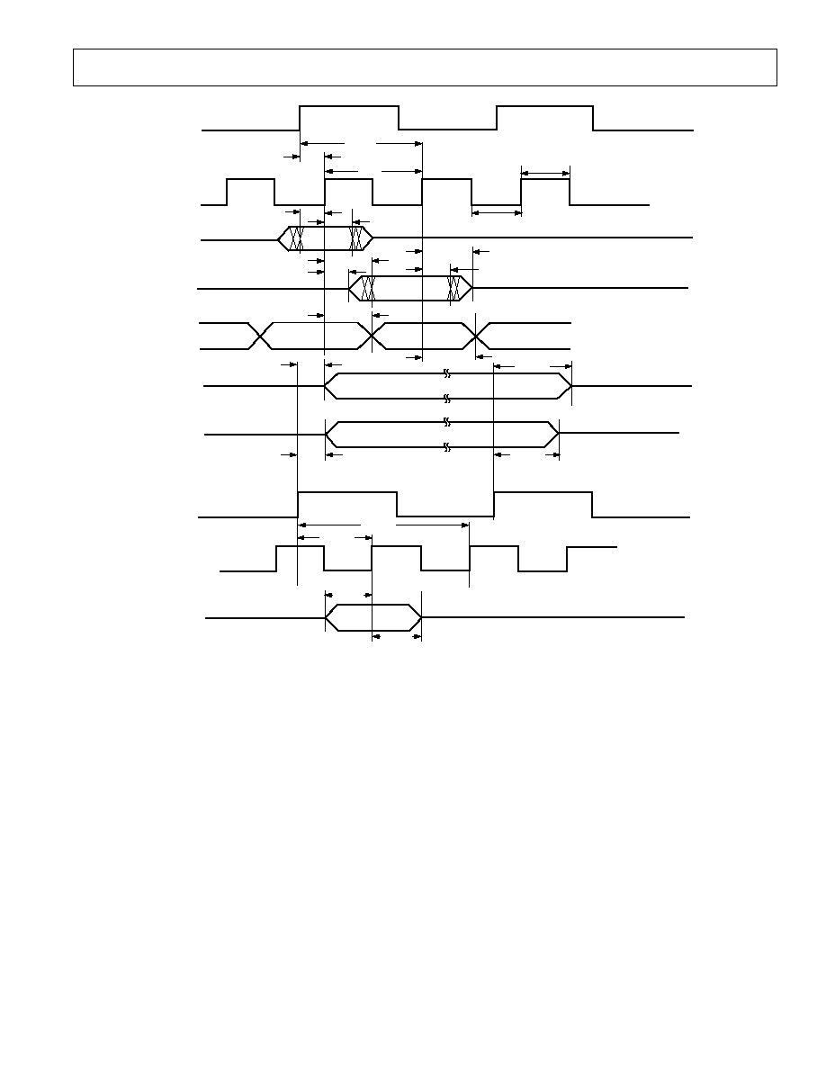
REV. B
ADSP-21065L
31
t
HCSDK
t
SCSDK
t
SSDKC1
t
SSDKC2
t
SDAEN
t
SDATR
t
SDCTR
t
HCADSDK
t
HCADSDK
t
SDTRSDK
t
DCADSDK
t
SDCEN
t
SDSDK
t
DCADSDK
t
SDENSDK
t
HDSDK
t
SDKL
t
SDKH
t
SDK
t
DSDK1
t
DSDK2
CLKIN
SDCLK
DATA
(IN)
DATA
(OUT)
CMND
1
ADDR
(OUT)
CMND
1
(OUT)
ADDR
(OUT)
SDCLK
(IN)
CMND
2
(IN)
CLKIN
NOTES
1
COMMAND = SDCKE,
MS
X
,
RAS, CAS, SDWE, DQM AND SDA10.
2
SDRAM CONTROLLER ADDS ONE SDRAM CLK THREE-STATED CYCLE DELAY (
t
CK
/2) ON A READ FOLLOWED BY A WRITE.
Figure 19. SDRAM Interface

REV. B
ADSP-21065L
32
Serial Ports
Parameter
Min
Max
Units
External Clock
Timing Requirements:
t
SFSE
TFS/RFS Setup Before TCLK/RCLK
1
4.0
ns
t
HFSE
TFS/RFS Hold After TCLK/RCLK
1
4.0
ns
t
SDRE
Receive Data Setup Before RCLK
1
1.5
ns
t
HDRE
Receive Data Hold After RCLK
1
4.0
ns
t
SCLKW
TCLK/RCLK Width
9.0
ns
t
SCLK
TCLK/RCLK Period
t
CK
ns
Internal Clock
Timing Requirements:
t
SFSI
TFS Setup Before TCLK
2
; RFS Setup Before RCLK
1
8.0
ns
t
HFSI
TFS/RFS Hold After TCLK/RCLK
1
1.0
ns
t
SDRI
Receive Data Setup Before RCLK
1
3.0
ns
t
HDRI
Receive Data Hold After RCLK
1
3.0
ns
External or Internal Clock
Switching Characteristics:
t
DFSE
RFS Delay After RCLK (Internally Generated RFS)
2
13.0
ns
t
HOFSE
RFS Hold After RCLK (Internally Generated RFS)
2
3.0
ns
External Clock
Switching Characteristics:
t
DFSE
TFS Delay After TCLK (Internally Generated TFS)
2
13.0
ns
t
HOFSE
TFS Hold After TCLK (Internally Generated TFS)
2
3.0
ns
t
DDTE
Transmit Data Delay After TCLK
2
12.5
ns
t
HDTE
Transmit Data Hold After TCLK
2
4.0
ns
Internal Clock
Switching Characteristics:
t
DFSI
TFS Delay After TCLK (Internally Generated TFS)
2
4.5
ns
t
HOFSI
TFS Hold After TCLK (Internally Generated TFS)
2
1.5
ns
t
DDTI
Transmit Data Delay After TCLK
2
7.5
ns
t
HDTI
Transmit Data Hold After TCLK
2
0.0
ns
t
SCLKIW
TCLK/RCLK Width
(t
SCLK
/2) 2.5
(t
SCLK
/2) + 2.5
ns
Enable and Three-State
Switching Characteristics:
t
DTENE
Data Enable from External TCLK
2
5.0
ns
t
DDTTE
Data Disable from External RCLK
2
10.0
ns
t
DTENI
Data Enable from Internal TCLK
2
0.0
ns
t
DDTTI
Data Disable from Internal TCLK
2
3.0
ns
t
DCLK
TCLK/RCLK Delay from CLKIN
18.0 + 6 DT
ns
t
DPTR
SPORT Disable After CLKIN
14.0
ns
External Late Frame Sync
t
DDTLFSE
Data Delay from Late External TFS or External RFS
with MCE = 1, MFD = 0
3, 4
10.5
ns
t
DTENLFSE
Data Enable from late FS or MCE = 1, MFD = 0
3, 4
3.5
ns
t
DDTLSCK
Data Delay from TCLK/RCLK for Late External
TFS or External RFS with MCE = 1, MFD = 0
3, 4
12.0
ns
t
DTENLSCK
Data Enable from RCLK/TCLK for Late External FS or
MCE = 1, MFD = 0
3, 4
4.5
ns
NOTES
To determine whether communication is possible between two devices at clock speed n, the following specifications must be confirmed: 1) frame sync delay and frame
sync setup-and-hold, 2) data delay and data setup-and-hold, and 3) SCLK width.
1
Referenced to sample edge.
2
Referenced to drive edge.
3
MCE = 1, TFS enable and TFS valid follow t
DDTENFS
and t
DDTLFSE.
4
If external RFS/TFS setup to RCLK/TCLK > t
SCLK
/2 then t
DDTLSCK
and t
DTENLSCK
apply; otherwise t
DDTLFSE
and t
DTENLFS
apply.
*Word selected timing for I
2
S mode is the same as TFS/RFS timing (normal framing only).
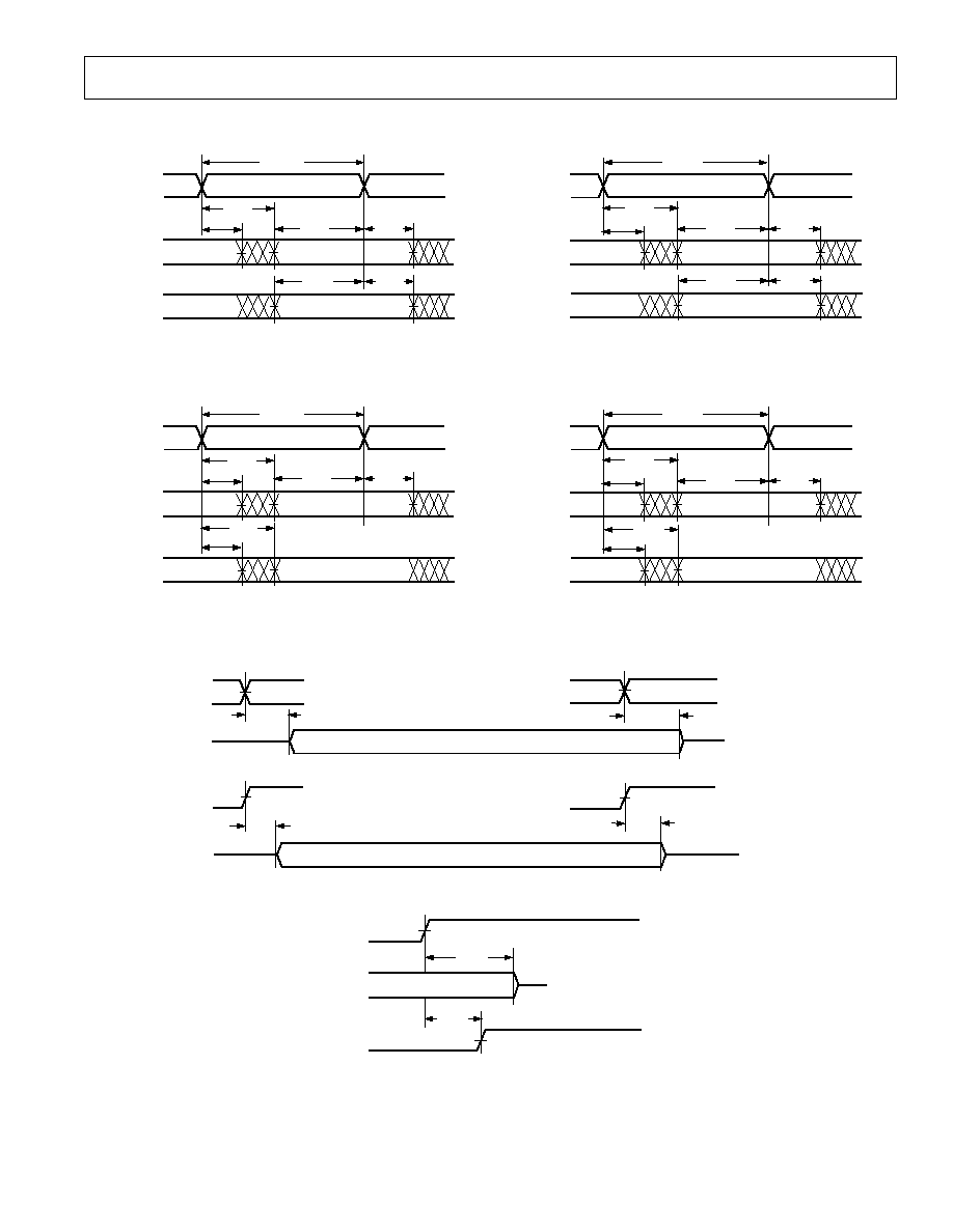
REV. B
ADSP-21065L
33
DT
DT
t
DDTTE
t
DDTEN
t
DDTTI
t
DDTIN
DRIVE
EDGE
DRIVE
EDGE
DRIVE
EDGE
DRIVE
EDGE
TCLK / RCLK
TCLK / RCLK
TCLK (EXT)
TFS ("LATE", EXT.)
t
SDRI
RCLK
RFS
DR
DRIVE
EDGE
SAMPLE
EDGE
t
HDRI
t
SFSI
t
HFSI
t
DFSE
t
HOFSE
t
SCLKIW
DATA RECEIVE INTERNAL CLOCK
t
SDRE
DATA RECEIVE EXTERNAL CLOCK
RCLK
RFS
DR
DRIVE
EDGE
SAMPLE
EDGE
t
HDRE
t
SFSE
t
HFSE
t
DFSE
t
SCLKW
t
HOFSE
NOTE: EITHER THE RISING EDGE OR FALLING EDGE OF RCLK, TCLK CAN BE USED AS THE ACTIVE SAMPLING EDGE.
t
DDTI
t
HDTI
TCLK
TFS
DT
DRIVE
EDGE
SAMPLE
EDGE
t
SFSI
t
HFSI
t
SCLKIW
t
DFSI
t
HOFSI
DATA TRANSMIT INTERNAL CLOCK
t
DDTE
t
HDTE
TCLK
TFS
DT
DRIVE
EDGE
SAMPLE
EDGE
t
SFSE
t
HFSE
t
DFSE
t
SCLKW
t
HOFSE
DATA TRANSMIT EXTERNAL CLOCK
CLKIN
SPORT ENABLE AND
THREE-STATE
LATENCY
IS TWO CYCLES
t
DPTR
SPORT DISABLE DELAY
FROM INSTRUCTION
t
DCLK
LOW TO HIGH ONLY
TCLK (INT)
RCLK (INT)
TCLK, RCLK
TFS, RFS, DT
NOTE: EITHER THE RISING EDGE OR FALLING EDGE OF RCLK OR TCLK CAN BE USED AS THE ACTIVE SAMPLING EDGE.
TCLK (INT)
TFS ("LATE", INT.)
Figure 20. Serial Ports
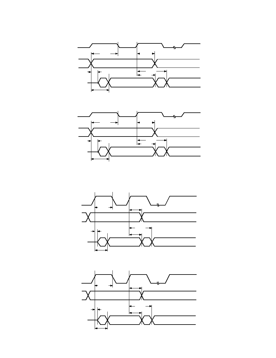
REV. B
ADSP-21065L
34
t
SFSE/I
DRIVE
SAMPLE
DRIVE
t
DTENLFSE
t
DDTLFSE
EXTERNAL RFS with MCE = 1, MFD = 0
1ST BIT
2ND BIT
DT
RCLK
RFS
LATE EXTERNAL TFS
t
HOFSE/I
t
HDTE/I
t
DDTE/I
t
SFSE/I
DRIVE
SAMPLE
DRIVE
t
DTENLFSE
t
DDTLFSE
1ST BIT
2ND BIT
DT
TCLK
TFS
t
HOFSE/I
t
HDTE/I
t
DDTE/I
Figure 21. External Late Frame Sync (Frame Sync Setup < t
SCLK
/2)
DRIVE
SAMPLE
DRIVE
t
DTENLSCK
EXTERNAL RFS with MCE = 1, MFD = 0
1ST BIT
2ND BIT
DT
RCLK
RFS
LATE EXTERNAL TFS
t
HOFSE/I
t
HDTE/I
t
DDTE/I
t
DDTLSCK
t
SFSE/I
DRIVE
SAMPLE
DRIVE
t
DTENLSCK
1ST BIT
2ND BIT
DT
TCLK
TFS
t
HOFSE/I
t
HDTE/I
t
DDTE/I
t
DDTLSCK
t
SFSE/I
Figure 22. External Late Frame Sync (Frame Sync Setup > t
SCLK
/2)
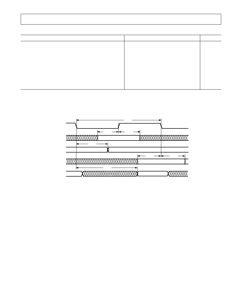
REV. B
ADSP-21065L
35
JTAG Test Access Port and Emulation
Parameter
Min
Max
Units
Timing Requirements:
t
TCK
TCK Period
t
CK
ns
t
STAP
TDI, TMS Setup Before TCK High
3.0
ns
t
HTAP
TDI, TMS Hold After TCK High
3.0
ns
t
SSYS
System Inputs Setup Before TCK Low
1
7.0
ns
t
HSYS
System Inputs Hold After TCK Low
1
12.0
ns
t
TRSTW
TRST Pulsewidth
4 t
CK
ns
Switching Characteristics:
t
DTDO
TDO Delay from TCK Low
11.0
ns
t
DSYS
System Outputs Delay After TCK Low
2
15.0
ns
NOTES
1
System Inputs = DATA
31-0
, ADDR
23-0
,
RD, WR, ACK, SBTS,
SW, HBR, HBG, CS, DMAR
1
,
DMAR
2
,
BR
2-1
, ID
1-0
,
IRQ
2-0
, FLAG
11-0
, DR0x, DR1x, TCLK0,
TCLK1, RCLK0, RCLK1, TFS0, TFS1, RFS0, RFS1, BSEL,
BMS, CLKIN, RESET, SDCLK
0
,
RAS, CAS, SDWE, SDCKE, PWM_EVENTx.
2
System Outputs = DATA
31-0
, ADDR
23-0
, MS
3-0
,
RD, WR, ACK, SW, HBG, REDY, DMAG1
,
DMAG2,
BR
2-1
,
CPA, FLAG
11-0
, PWM_EVENTx, DT0x, DT1x,
TCLK0, TCLK1, RCLK0, RCLK1, TFS0, TFS1, RFS0, RFS1,
BMS, SDCLK0, SDCLK1, DQM, SDA10, RAS, CAS, SDWE, SDCKE, BM, XTAL.
TCK
t
STAP
t
TCK
t
HTAP
t
DTDO
t
SSYS
t
HSYS
t
DSYS
TMS
TDI
TDO
SYSTEM
INPUTS
SYSTEM
OUTPUTS
Figure 23. JTAG Test Access Port and Emulation
REV. B
ADSP-21065L
36
OUTPUT DRIVE CURRENT
SOURCE VOLTAGE V
80
0
3.50
SOURCE CURRENT
mA
0.50
1.00
1.50
2.00
2.50
3.00
60
40
100
120
20
20
40
0
80
60
3.3V, +25 C
3.6V, 40 C
3.1V, +100 C
3.6V, 40 C
V
OL
V
OH
3.1V, +85 C
3.1V, +100 C
3.1V, +85 C
3.3V, +25 C
Figure 24. Typical Drive Currents
TEST CONDITIONS
Output Disable Time
Output pins are considered to be disabled when they stop driv-
ing, go into a high impedance state, and start to decay from
their output high or low voltage. The time for the voltage on the
bus to decay by
V is dependent on the capacitive load, C
L
and
the load current, I
L
. This decay time can be approximated by
the following equation:
t
C
V
I
DECAY
L
L
=
×
The output disable time t
DIS
is the difference between t
MEASURED
and t
DECAY
as shown in Figure 26. The time t
MEASURED
is the
interval from when the reference signal switches to when the
output voltage decays
V from the measured output high or
output low voltage. t
DECAY
is calculated with test loads C
L
and
I
L
, and with
V equal to 0.5 V.
Output Enable Time
Output pins are considered to be enabled when they have made
a transition from a high impedance state to when they start
driving. The output enable time t
ENA
is the interval from when a
reference signal reaches a high or low voltage level to when the
output has reached a specified high or low trip point, as shown
in the Output Enable/Disable diagram. If multiple pins (such as
the data bus) are enabled, the measurement value is that of the
first pin to start driving.
Example System Hold Time Calculation
To determine the data output hold time in a particular system,
first calculate t
DECAY
using the equation given above. Choose
V
to be the difference between the ADSP-21065L's output voltage
and the input threshold for the device requiring the hold time. A
typical
V will be 0.4 V. C
L
is the total bus capacitance (per
data line), and I
L
is the total leakage or three-state current (per
data line). The hold time will be t
DECAY
plus the minimum
disable time (i.e., t
DATRWH
for the write cycle).
REFERENCE
SIGNAL
t
DIS
OUTPUT STARTS
DRIVING
V
OH (MEASURED)
V
V
OL (MEASURED)
+ V
t
MEASURED
V
OH (MEASURED)
V
OL (MEASURED)
2.0V
1.0V
V
OH (MEASURED)
V
OL (MEASURED)
HIGH-IMPEDANCE STATE.
TEST CONDITIONS CAUSE
THIS VOLTAGE TO BE
APPROXIMATELY 1.5V
OUTPUT STOPS
DRIVING
t
ENA
t
DECAY
OUTPUT
Figure 25. Output Enable
+1.5V
50pF
TO
OUTPUT
PIN
I
OL
I
OH
Figure 26. Equivalent Device Loading for AC Measure-
ments (Includes All Fixtures)
INPUT OR
OUTPUT
1.5V
1.5V
Figure 27. Voltage Reference Levels for AC Measure-
ments (Except Output Enable/Disable)
REV. B
ADSP-21065L
37
Capacitive Loading
Output delays and holds are based on standard capacitive loads:
50 pF on all pins. The delay and hold specifications given
should be derated by a factor of l.8 ns/50 pF for loads other
than the nominal value of 50 pF. Figure 28 and Figure 29 show
how output rise time varies with capacitance. Figure 30 shows
graphically how output delays and hold vary with load capaci-
tance. (Note that this graph or derating does not apply to output
disable delays; see the previous section Output Disable time
under Test Conditions.) The graphs of Figure 28, Figure 29
and Figure 30 may not be linear outside the ranges shown.
LOAD CAPACITANCE pF
0
0
200
20
RISE AND FALL TIMES
ns
40
60
80
100
120
140
160
180
2
RISE TIME
FALL TIME
4
6
8
10
12
14
16
18
Figure 28. Typical Rise and Fall Time (10%90% V
DD
)
LOAD CAPACITANCE pF
8.0
4.0
0
0
200
20
RISE AND FALL TIMES
ns
40
60
80
100
120
140
160
180
7.0
6.0
2.0
1.0
5.0
3.0
RISE TIME
FALL TIME
Figure 29. Typical Rise and Fall Time (0.8 V2.0 V)
LOAD CAPACITANCE pF
OUTPUT DELAY OR HOLD
ns
5
2
0
140
20
40
60
80
100
120
4
3
2
1
0
1
160
180
200
6
Figure 30. Typical Output Delay or Hold
REV. B
ADSP-21065L
38
POWER DISSIPATION
Total power dissipation has two components: one due to inter-
nal circuitry and one due to the switching of external output
drivers. Internal power dissipation depends on the sequence in
which instructions execute and the data operands involved. See
I
DDIN
calculation in Electrical Characteristics section. Internal
power dissipation is calculated this way:
P
INT
= I
DDIN
× V
DD
The external component of total power dissipation is caused by
the switching of output pins. Its magnitude depends on:
the number of output pins that switch during each cycle (O)
the maximum frequency at which the pins can switch (f)
the load capacitance of the pins (C)
the voltage swing of the pins (V
DD
).
The external component is calculated using:
P
EXT
= O
× C × V
DD
2
× f
The load capacitance should include the processor's package
capacitance (C
IN
). The frequency f includes driving the load
high and then back low. Address and data pins can drive high
and low at a maximum rate of 1/t
CK
while in SDRAM burst
mode.
Example:
Estimate P
EXT
with the following assumptions:
a system with one bank of external memory (32-bit)
two 1M
× 16 SDRAM chips, each with a control signal load
of 3 pF and a data signal load of 4 pF
external data writes occur in burst mode, two every 1/t
CK
cycles, a potential frequency of 1/t
CK
cycles/s. Assume 50%
pin switching
the external SDRAM clock rate is 60 MHz (2/t
CK
).
The P
EXT
equation is calculated for each class of pins that can
drive:
Table V. External Power Calculations
Pin
# of
%
Type
Pins Switching
C
f
V
DD
2
= P
EXT
Address
11
50
× 10.7 × 30 MHz × 10.9 V = 0.019 W
MS
0
1
0
× 10.7 --
× 10.9 V = 0.000 W
SDWE
1
0
× 10.7 --
× 10.9 V = 0.000 W
Data
32
50
× 7.7
× 30 MHz × 10.9 V = 0.042 W
SDRAM CLK 1
× 10.7 × 30 MHz × 10.9 V = 0.007 W
P
EXT
= 0.068 W
A typical power consumption can now be calculated for these
conditions by adding a typical internal power dissipation. (I
DDIN
see calculation in Electrical Characteristics section):
P
TOTAL
= P
EXT
+ (I
DDIN
× V
DD
)
Note that the conditions causing a worst-case P
EXT
differ from
those causing a worst-case P
INT
. Maximum P
INT
cannot occur
while 100% of the output pins are switching from all ones (1s)
to all zeros (0s). Note also that it is not common for an appli-
cation to have 100% or even 50% of the outputs switching
simultaneously.
ENVIRONMENTAL CONDITIONS
Thermal Characteristics
The ADSP-21065L is offered in a 208-lead MQFP and a 196-
ball Mini-BGA package.
The ADSP-21065L is specified for a case temperature (T
CASE
)
.
To ensure that T
CASE
is not exceeded, an air flow source may be
used.
T
CASE
= T
AMB
+ (PD
×
CA
)
T
CASE
= Case temperature (measured on top surface of package)
PD =
Power Dissipation in W (this value depends upon the
specific application; a method for calculating PD is
shown under Power Dissipation)
JC
=
7.1
°C/W for 208-lead MQFP
JC
=
5.1
°C/W for 196-ball Mini-BGA
Airflow
Table VI. Thermal Characteristics (208-Lead MQFP)
(Linear Ft./Min.)
0
100
200
400
600
CA
(
°C/W)
24
20
19
17
13
Table VII. 196-Ball Mini-BGA
(Linear Ft./Min.)
0
200
400
CA
(
°C/W)
38
29
23

REV. B
ADSP-21065L
39
Pin
Pin
Pin
Pin
Pin
Pin
Pin
Pin
Pin
Pin
No.
Name
No.
Name
No.
Name
No.
Name
No.
Name
1
VDD
43
CAS
85
VDD
127
DATA28
169
ADDR17
2
RFS0
44
SDWE
86
DATA3
128
DATA29
170
ADDR16
3
GND
45
VDD
87
DATA4
129
GND
171
ADDR15
4
RCLK0
46
DQM
88
DATA5
130
VDD
172
VDD
5
DR0A
47
SDCKE
89
GND
131
VDD
173
ADDR14
6
DR0B
48
SDA10
90
DATA6
132
DATA30
174
ADDR13
7
TFS0
49
GND
91
DATA7
133
DATA31
175
ADDR12
8
TCLK0
50
DMAG1
92
DATA8
134
FLAG7
176
VDD
9
VDD
51
DMAG2
93
VDD
135
GND
177
GND
10
GND
52
HBG
94
GND
136
FLAG6
178
ADDR11
11
DT0A
53
BMSTR
95
VDD
137
FLAG5
179
ADDR10
12
DT0B
54
VDD
96
DATA9
138
FLAG4
180
ADDR9
13
RFS1
55
CS
97
DATA10
139
GND
181
GND
14
GND
56
SBTS
98
DATA11
140
VDD
182
VDD
15
RCLK1
57
GND
99
GND
141
VDD
183
ADDR8
16
DR1A
58
WR
100
DATA12
142
NC
184
ADDR7
17
DR1B
59
RD
101
DATA13
143
ID1
185
ADDR6
18
TFS1
60
GND
102
NC
144
ID0
186
GND
19
TCLK1
61
VDD
103
NC
145
EMU
187
GND
20
VDD
62
GND
104
DATA14
146
TDO
188
ADDR5
21
VDD
63
REDY
105
VDD
147
TRST
189
ADDR4
22
DT1A
64
SW
106
GND
148
TDI
190
ADDR3
23
DT1B
65
CPA
107
DATA15
149
TMS
191
VDD
24
PWM_EVENT1
66
VDD
108
DATA16
150
GND
192
VDD
25
GND
67
VDD
109
DATA17
151
TCK
193
ADDR2
26
PWM_EVENT0
68
GND
110
VDD
152
BSEL
194
ADDR1
27
BR1
69
ACK
111
DATA18
153
BMS
195
ADDR0
28
BR2
70
MS0
112
DATA19
154
GND
196
GND
29
VDD
71
MS1
113
DATA20
155
GND
197
FLAG0
30
CLKIN
72
GND
114
GND
156
VDD
198
FLAG1
31
XTAL
73
GND
115
NC
157
RESET
199
FLAG2
32
VDD
74
MS2
116
DATA21
158
VDD
200
VDD
33
GND
75
MS3
117
DATA22
159
GND
201
FLAG3
34
SDCLK1
76
FLAG11
118
DATA23
160
ADDR23
202
NC
35
GND
77
VDD
119
GND
161
ADDR22
203
NC
36
VDD
78
FLAG10
120
VDD
162
ADDR21
204
GND
37
SDCLK0
79
FLAG9
121
DATA24
163
VDD
205
IRQ0
38
DMAR1
80
FLAG8
122
DATA25
164
ADDR20
206
IRQ1
39
DMAR2
81
GND
123
DATA26
165
ADDR19
207
IRQ2
40
HBR
82
DATA0
124
VDD
166
ADDR18
208
NC
41
GND
83
DATA1
125
GND
167
GND
42
RAS
84
DATA2
126
DATA27
168
GND
208-LEAD MQFP PIN CONFIGURATION
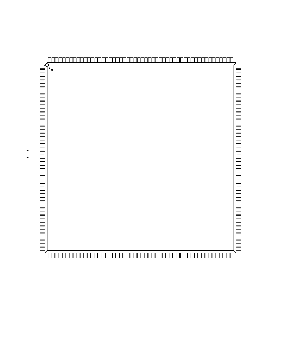
REV. B
ADSP-21065L
40
208-LEAD MQFP PIN
208
207
206
205
204
203
202
201
200
199
198
197
196
195
194
193
192
191
189
188
187
186
185
184
183
182
181
180
190
179
178
177
175
174
173
172
171
170
176
169
168
167
165
164
163
162
161
160
159
158
157
166
71
72
73
74
75
76
77
78
79
80
53
54
55
56
57
58
59
60
61
62
63
64
65
66
67
68
69
70
81
82
83
84
86
87
88
89
90
85
91
92
93
94
96
97
98
99
95
10
0
10
1
102
103
104
5
4
3
2
7
6
9
8
1
14
13
12
11
16
15
17
10
19
18
23
22
21
20
25
24
27
26
29
28
32
31
30
34
33
36
35
40
39
38
37
41
43
42
45
44
50
49
48
47
46
52
51
152
153
154
155
150
151
156
148
149
143
144
145
146
141
142
140
147
138
139
134
135
136
137
132
133
130
131
128
129
125
126
127
123
124
121
122
120
117
118
119
116
114
115
112
113
107
108
109
110
111
105
106
OO
BMSTR
PIN 1
IDENTIFIER
TOP VIEW
(Not to Scale)
VDD
CS
SBTS
GND
WR
RD
GND
VDD
GND
REDY
SW
CPA
VDD
VDD
GND
ACK
MS
0
MS
1
GND
GND
MS
2
MS
3
FLAG11
VDD
FLAG10
FLAG9
FLAG8
GND
DATA0
DATA1
DATA2
VDD
DATA3
DATA4
DATA5
GND
DATA6
DATA7
DATA8
VDD
GND
VDD
DATA9
DATA10
DATA11
GND
DATA12
DATA13
NC
NC
DATA14
NC
IRQ
2
IRQ
1
IRQ
0
GND
NC
NC
FLAG3
VDD
VDD
RSF0
GND
RCLK0
DR0A
DR0B
TFS0
TCLK0
VDD
GND
DT0A
DT0B
RFS1
GND
RCLK1
DR1A
DR1B
TFS1
TCLK1
VDD
VDD
DT1A
DT1B
PWM EVENT1
GND
PWM EVENT0
BR1
BR2
VDD
CLKIN
XTAL
VDD
GND
SDCLK1
GND
VDD
SDCLK0
DMAR1
DMAR2
HBR
GND
RAS
SDWE
VDD
DQM
SDCKE
SDA10
GND
DMAG1
DMAG2
HBG
GND
GND
BMS
BSEL
TCK
GND
TMS
TDI
TRST
TDO
EMU
ID0
ID1
NC
VDD
VDD
GND
GND
VDD
VDD
GND
GND
VDD
VDD
GND
GND
VDD
DATA15
GND
VDD
VDD
FLAG2
FLAG1
FLAG0
GND
ADDR0
ADDR1
ADDR2
VDD
VDD
ADDR3
ADDR4
ADDR5
GND
GND
ADDR6
ADDR7
ADDR8
VDD
GND
ADDR9
ADDR10
ADDR11
GND
VDD
ADDR12
ADDR13
ADDR14
VDD
ADDR15
ADDR16
ADDR17
GND
GND
ADDR18
ADDR19
ADDR20
VDD
ADDR21
ADDR22
ADDR23
GND
VDD
RESET
ADSP-21065L
CAS
DATA16
DATA17
DATA18
DATA19
DATA20
DATA22
DATA21
NC
DATA23
DATA24
DATA25
DATA26
DATA27
DATA28
DATA29
DATA30
DATA31
FLAG7
FLAG6
FLAG5
FLAG4
NC = NO CONNECT
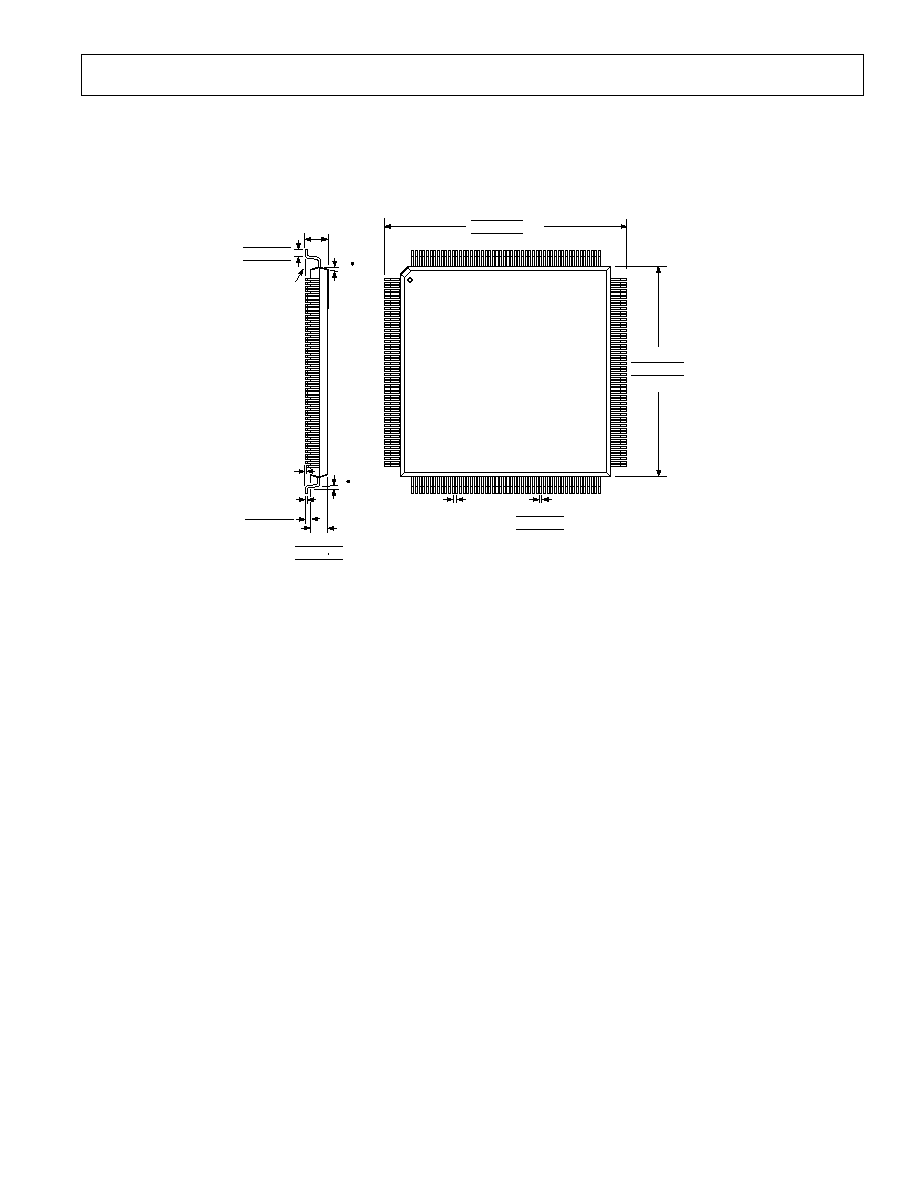
REV. B
ADSP-21065L
41
OUTLINE DIMENSIONS
Dimensions shown in inches and (mm).
208-Lead Plastic Quad Flatpack (MQFP)
1
208
157
156
105
104
53
52
TOP VIEW
(PINS DOWN)
0.020 (0.50)
BSC
1.213 (30.80)
1.205 (30.60) SQ
1.197 (30.40)
1.106 (28.10)
1.102 (28.00) SQ
1.098 (27.90)
0.011 (0.27)
0.009 (0.22)
0.007 (0.17)
LEAD PITCH
LEAD WIDTH
SEATING
PLANE
0.161 (4.10)
MAX
0.003 (0.08)
MAX LEAD
COPLANARITY
0.020 (0.50)
0.010 (0.25)
0.141 (3.59)
0.137 (3.49)
0.133 (3.39)
0.007 (0.17) MAX
0
MIN
10
TYP
0.030 (0.75)
0.024 (0.60)
0.020 (0.50)
NOTES
1. THE ACTUAL POSITION OF EACH LEAD IS WITHIN 0.003 (0.08) FROM ITS IDEAL
POSITION WHEN MEASURED IN THE LATERAL DIRECTION.
2. CENTER FIGURES ARE TYPICAL UNLESS OTHERWISE NOTED.
3. THE 208 LEAD MQFP IS A METRIC PACKAGE. ENGLISH DIMENSIONS PROVIDED
ARE APPROXIMATE AND MUST NOT BE USED FOR BOARD DESIGN PURPOSES.

REV. B
ADSP-21065L
42
196-BALL MINI-BGA PIN CONFIGURATION
Ball #
Name
Ball #
Name
Ball #
Name
Ball #
Name
Ball #
Name
A1
NC1
B1
DR0A
C1
TCLK0
D1
RCLK1
E1
TFS1
A2
NC2
B2
RFS0
C2
RCLK0
D2
TFS0
E2
DT0B
A3
FLAG2
B3
IRQ0
C3
IRQ2
D3
DR0B
E3
DT0A
A4
ADDR0
B4
FLAG0
C4
FLAG3
D4
IRQ1
E4
RFS1
A5
ADDR3
B5
ADDR2
C5
ADDR1
D5
FLAG1
E5
VDD
A6
ADDR6
B6
ADDR5
C6
ADDR4
D6
VDD
E6
GND
A7
ADDR7
B7
ADDR9
C7
ADDR10
D7
VDD
E7
GND
A8
ADDR8
B8
ADDR12
C8
ADDR13
D8
VDD
E8
GND
A9
ADDR11
B9
ADDR15
C9
ADDR16
D9
VDD
E9
GND
A10
ADDR14
B10
ADDR19
C10
ADDR20
D10
VDD
E10
VDD
A11
ADDR17
B11
ADDR21
C11
ADDR22
D11
BMS
E11
ID0
A12
ADDR18
B12
ADDR23
C12
RESET
D12
TMS
E12
TDI
A13
NC8
B13
GND
C13
BSEL
D13
TRST
E13
ID1
A14
NC7
B14
TCK
C14
TDO
D14
EMU
E14
FLAG4
F1
TCLK1
G1
PWM_
H1
PWM_
J1
CLKIN
K1
DMAR1
EVENT1
EVENT0
F2
DR1B
G2
DT1B
H2
BR1
J2
XTAL
K2
SDCLK0
F3
DR1A
G3
DT1A
H3
BR2
J3
SDCLK1
K3
HBR
F4
VDD
G4
VDD
H4
VDD
J4
VDD
K4
SDWE
F5
GND
G5
GND
H5
GND
J5
GND
K5
VDD
F6
GND
G6
GND
H6
GND
J6
GND
K6
GND
F7
GND
G7
GND
H7
GND
J7
GND
K7
GND
F8
GND
G8
GND
H8
GND
J8
GND
K8
GND
F9
GND
G9
GND
H9
GND
J9
GND
K9
GND
F10
GND
G10
GND
H10
GND
J10
GND
K10
VDD
F11
VDD
G11
VDD
H11
VDD
J11
VDD
K11
DATA19
F12
FLAG6
G12
DATA31
H12
DATA28
J12
DATA24
K12
DATA21
F13
FLAG5
G13
DATA30
H13
DATA27
J13
DATA25
K13
DATA20
F14
FLAG7
G14
DATA29
H14
DATA26
J14
DATA23
K14
DATA22
L1
DMAR2
M1
RAS
N1
DQM
P1
NC3
L2
CAS
M2
SDCKE
N2
HBG
P2
NC4
L3
SDA10
M3
DMAG1
N3
BMSTR
P3
GND
L4
DMAG2
M4
CS
N4
SBTS
P4
WR
L5
VDD
M5
RD
N5
REDY
P5
SW
L6
VDD
M6
CPA
N6
GND
P6
MS0
L7
VDD
M7
ACK
N7
MS1
P7
MS2
L8
VDD
M8
FLAG10
N8
FLAG11
P8
MS3
L9
VDD
M9
DATA2
N9
DATA1
P9
FLAG9
L10
DATA8
M10
DATA5
N10
DATA4
P10
FLAG8
L11
DATA13
M11
DATA9
N11
DATA7
P11
DATA0
L12
DATA16
M12
DATA12
N12
DATA10
P12
DATA3
L13
DATA17
M13
DATA14
N13
DATA11
P13
DATA6
L14
DATA18
M14
DATA15
N14
NC6
P14
NC5

REV. B
ADSP-21065L
43
196-BALL MINI-BGA PIN CONFIGURATION
14
13
12
11
10
9
8
7
6
5
4
3
2
1
A
B
C
D
E
F
G
H
J
K
L
M
N
P
NC7
TCK
TDO
EMU
FLAG4
FLAG7
DATA29
DATA26
DATA23
DATA22
DATA18
DATA15
NC6
NC5
NC8
GND
BSEL
TRST
ID1
FLAG5
DATA30
DATA27
DATA25
DATA20
DATA17
DATA14
DATA11
DATA6
ADDR18
ADDR23
RESET
TMS
TDI
FLAG6
DATA31
DATA28
DATA24
DATA21
DATA16
DATA12
DATA10
DATA3
ADDR17
ADDR21
ADDR22
BMS
ID0
VDD
VDD
VDD
VDD
DATA19
DATA13
DATA9
DATA7
DATA0
ADDR14
ADDR19
ADDR20
VDD
VDD
GND
GND
GND
GND
VDD
DATA8
DATA5
DATA4
FLAG8
ADDR11
ADDR15
ADDR16
VDD
GND
GND
GND
GND
GND
GND
VDD
DATA2
DATA1
FLAG9
ADDR8
ADDR12
ADDR13
VDD
GND
GND
GND
GND
GND
GND
VDD
FLAG10
FLAG11
MS3
ADDR7
ADDR9
ADDR10
VDD
GND
GND
GND
GND
GND
GND
VDD
ACK
MS1
MS2
ADDR6
ADDR5
ADDR4
VDD
GND
GND
GND
GND
GND
GND
VDD
CPA
GND
MS0
ADDR3
ADDR2
ADDR1
FLAG1
VDD
GND
GND
GND
GND
VDD
VDD
RD
REDY
SW
ADDR0
FLAG0
FLAG3
IRQ1
RFS1
VDD
VDD
VDD
VDD
SDWE
DMAG2
CS
SBTS
WR
FLAG2
IRQ0
IRQ2
DR0B
DT0A
DR1A
DT1A
BR2
SDCLK1
HBR
SDA10
DMAG1
BMSTR
GND
NC2
RFS0
RCLK0
TFS0
DT0B
DR1B
DT1B
BR1
XTAL
SDCLK0
CAS
SDCKE
HBG
NC4
NC1
DR0A
TCLK0
RCLK1
TFS1
TCLK1
PWM_
EVENT1
PWM_
EVENT0
CLKIN
DMAR1
DMAR2
RAS
DQM
NC3
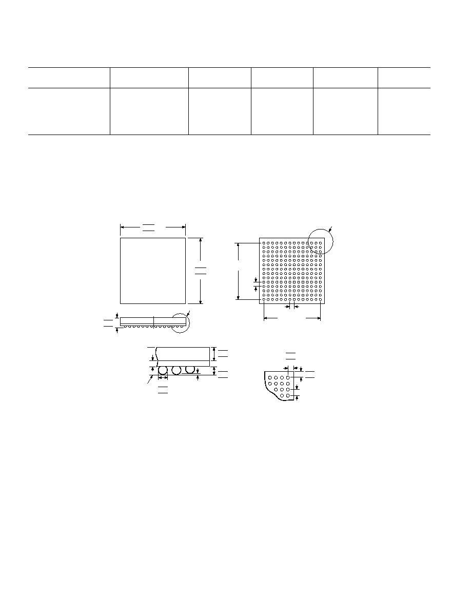
REV. B
ADSP-21065L
44
C3533b35/00 (rev. B) 00172
PRINTED IN U.S.A.
OUTLINE DIMENSIONS
Dimensions shown in mm.
196-Ball Mini-BGA
0.70
0.60
0.50
BALL
DIAMETER
1.90
1.75
1.60
1.10
1.00
0.90
1.00
BSC
1.10
1.00
0.90
DETAIL B
DETAIL A
SEATING
PLANE
0.75
0.70
0.65
0.60
0.50
0.40
DETAIL A
0.55
NOM
0.20
MAX BALL
COPLANARITY
CCC = 0.25
(TOP PLANARITY)
13.00 BSC
A
B
C
D
E
F
G
H
J
K
L
M
N
P
14 13 12 11 10 9 8 7 6 5 4 3 2 1
DETAIL B
13.00
BSC
1.00 BSC
1.00
BSC
TOP VIEW
15.20
15.00 SQ
14.80
TOP VIEW
15.20
15.00 SQ
14.80
NOTES
1. THE ACTUAL POSITION OF THE BALL GRID IS WITHIN 0.30 OF ITS IDEAL POSITION RELATIVE TO THE
PACKAGE EDGES. THE ACTUAL POSITION OF EACH BALL IS WITHIN 0.10 OF ITS IDEAL POSITION
RELATIVE TO THE BALL GRID.
2.
ALL MEASUREMENTS ARE PROVIDED IN METRIC UNITS BECAUSE THIS IS A METRIC PACKAGE.
ANALOG DEVICES STRONGLY RECOMMENDS THAT YOU DESIGN WITH THE METRIC MEASUREMENTS
ONLY.
3. BALL DIAMETER HAS BEEN CHANGED FROM 0.50mm NOMINAL TO 0.60mm NOMINAL TO COMPLY
WITH JEDEC STANDARD PUBLICATION 95 CASE OUTLINE DRAWING MO151. 0.60 NOMINAL BALL
DIAMETER PRODUCT WILL BE AVAILABLE IN JULY, 2000.
ORDERING GUIDE
Part
Case Temperature
Instruction
On-Chip
Operating
Package
Number
Range
Rate
SRAM
Voltage
Options
ADSP-21065LKS-240
0
°C to +85°C
60 MHz
544 Kbit
3.3 V
MQFP
ADSP-21065LCS-240
40
°C to +100°C
60 MHz
544 Kbit
3.3 V
MQFP
ADSP-21065LKCA-240
0
°C to +85°C
60 MHz
544 Kbit
3.3 V
Mini-BGA
ADSP-21065LKS-264
0
°C to +85°C
66 MHz
544 Kbit
3.3 V
MQFP
ADSP-21065LKCA-264
0
°C to +85°C
66 MHz
544 Kbit
3.3 V
Mini-BGA