 | ÐлекÑÑоннÑй компоненÑ: SMP04 | СкаÑаÑÑ:  PDF PDF  ZIP ZIP |
Äîêóìåíòàöèÿ è îïèñàíèÿ www.docs.chipfind.ru
REV. D
Information furnished by Analog Devices is believed to be accurate and
reliable. However, no responsibility is assumed by Analog Devices for its
use, nor for any infringements of patents or other rights of third parties
which may result from its use. No license is granted by implication or
otherwise under any patent or patent rights of Analog Devices.
a
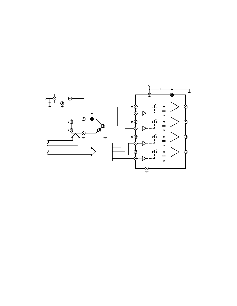
CMOS Quad
Sample-and-Hold Amplifier
FUNCTIONAL BLOCK DIAGRAM
V
SS
V
OUT1
V
OUT2
V
OUT3
V
OUT4
V
SS
DGND
V
IN1
S
/H
1
V
IN2
V
IN3
V
IN4
S
/H
2
S
/H
3
S
/H
4
V
DD
V
SS
V
SS
V
SS
SMP04
FEATURES
Four Independent Sample-and-Holds
Internal Hold Capacitors
High Accuracy: 12 Bit
Very Low Droop Rate: 2 mV/s typ
Output Buffers Stable for C
L
500 pF
TTL/CMOS Compatible Logic Inputs
Single or Dual Supply Applications
Monolithic Low Power CMOS Design
APPLICATIONS
Signal Processing Systems
Multichannel Data Acquisition Systems
Automatic Test Equipment
Medical and Analytical Instrumentation
Event Analysis
DAC Deglitching
The SMP04 offers significant cost and size reduction over
equivalent module or discrete designs. It is available in a
16-lead hermetic or plastic DIP and surface mount SOIC
packages. It is specified over the extended industrial tem-
perature range of 40
°
C to +85
°
C.
GENERAL DESCRIPTION
The SMP04 is a monolithic quad sample-and-hold; it has four
internal precision buffer amplifiers and internal hold capacitors.
It is manufactured in ADI's advanced oxide isolated CMOS
technology to obtain the high accuracy, low droop rate and fast
acquisition time required by data acquisition and signal process-
ing systems. The device can acquire an 8-bit input signal to
±
1/2 LSB in less than four microseconds. The SMP04 can
operate from single or dual power supplies with TTL/CMOS
logic compatibility. Its output swing includes the negative supply.
The SMP04 is ideally suited for a wide variety of sample-and-
hold applications, including amplifier offset or VCA gain adjust-
ments. One or more can be used with single or multiple DACs
to provide multiple setpoints within a system.
One Technology Way, P.O. Box 9106, Norwood, MA 02062-9106, U.S.A.
Tel: 781/329-4700
World Wide Web Site: http://www.analog.com
Fax: 781/326-8703
© Analog Devices, Inc., 1998
SMP04*
*Protected by U.S. Patent No. 4,739,281.
SMP04SPECIFICATIONS
ELECTRICAL CHARACTERISTICS
Parameter
Symbol
Conditions
Min
Typ
Max
Units
Linearity Error
0.01
%
Buffer Offset Voltage
V
OS
V
IN
= 6 V
10
±
2.5
+10
mV
Hold Step
V
HS
V
IN
= 6 V, T
A
= +25
°
C to +85
°
C
2.5
4
mV
V
IN
= 6 V, T
A
= 40
°
C
5
mV
Droop Rate
V/
t
V
IN
= 6 V, T
A
= +25
°
C
2
25
mV/s
Output Source Current
1
I
SOURCE
V
IN
= 6 V
1.2
mA
Output Sink Current
1
I
SINK
V
IN
= 6 V
0.5
mA
Output Voltage Range
OVR
R
L
= 20 k
0.06
10.0
V
R
L
= 10 k
0.06
9.5
V
LOGIC CHARACTERISTICS
Logic Input High Voltage
V
INH
2.4
V
Logic Input Low Voltage
V
INL
0.8
V
Logic Input Current
I
IN
0.5
1
µ
A
DYNAMIC PERFORMANCE
2
Acquisition Time
3
t
AQ
T
A
= +25
°
C, 0 V to 10 V Step to 0.1%
3.5
4.25
µ
s
40
°
C
T
A
+85
°
C
3.75
5.25
µ
s
Acquisition Time
3
t
AQ
T
A
= +25
°
C, 0 V to 10 V Step to 0.01%
9
µ
s
Hold Mode Settling Time
t
H
To 1 mV
1
µ
s
Slew Rate
4
SR
R
L
= 20 k
3
4
V/
µ
s
Capacitive Load Stability
C
L
<30% Overshoot
500
pF
Analog Crosstalk
0 V to 10 V Step
80
dB
SUPPLY CHARACTERISTICS
Power Supply Rejection Ratio
PSRR
10.8 V
V
DD
13.2 V
60
75
dB
Supply Current
I
DD
4
7
mA
Power Dissipation
P
DIS
84
mW
ELECTRICAL CHARACTERISTICS
Parameter
Symbol
Conditions
Min
Typ
Max
Units
Linearity Error
0.01
%
Buffer Offset Voltage
V
OS
V
IN
= 0 V
10
±
2.5
+10
mV
Hold Step
V
HS
V
IN
= 0 V, T
A
= +25
°
C to +85
°
C
2.5
4
mV
V
IN
= 0 V, T
A
= 40
°
C
5
mV
Droop Rate
V/
t
V
IN
= 0 V, T
A
= +25
°
C
2
25
mV/s
Output Resistance
R
OUT
1
Output Source Current
1
I
SOURCE
V
IN
= 0 V
1.2
mA
Output Sink Current
1
I
SINK
V
IN
= 0 V
0.5
mA
Output Voltage Range
OVR
R
L
= 20 k
3.0
+3.0
V
LOGIC CHARACTERISTICS
Logic Input High Voltage
V
INH
2.4
V
Logic Input Low Voltage
V
INL
0.8
V
Logic Input Current
I
IN
0.5
1
µ
A
DYNAMIC PERFORMANCE
2
Acquisition Time
3
t
AQ
3 V to +3 V Step to 0.1%
3.6
11
µ
s
Acquisition Time
3
t
AQ
3 V to +3 V Step to 0.01%
9
µ
s
Hold Mode Settling Time
t
H
To 1 mV
1
µ
s
Slew Rate
5
SR
R
L
= 20 k
3
V/
µ
s
Capacitive Load Stability
C
L
<30% Overshoot
500
pF
SUPPLY CHARACTERISTICS
Power Supply Rejection Ratio
PSRR
±
5 V
V
DD
±
6 V
60
75
dB
Supply Current
I
DD
3.5
5.5
mA
Power Dissipation
P
DIS
55
mW
NOTES
1
Outputs are capable of sinking and sourcing over 20 mA, but linearity and offset are guaranteed at specified load levels.
2
All input control signals are specified with t
R
= t
F
= 5 ns (10% to 90% of +5 V) and timed from a voltage level of 1.6 V.
3
This parameter is guaranteed without test.
4
Slew rate is measured in the sample mode with a 0 V to 10 V step from 20% to 80%.
5
Slew rate is measured in the sample mode with a 3 V to +3 V step from 20% to 80%.
Specifications are subject to change without notice.
REV. D
2
(@ V
DD
= +12.0 V, V
SS
= DGND = 0 V, R
L
= No Load, T
A
= Operating Temperature Range
specified in Absolute Maximum Ratings, unless otherwise noted.)
(@ V
DD
= +5.0 V, V
SS
= 5.0 V, DGND = 0.0 V, R
L
= No Load, T
A
= Operating Temperature
Range specified in Absolute Maximum Ratings, unless otherwise noted.)
SMP04
3
REV. D
ABSOLUTE MAXIMUM RATINGS
(T
A
= +25
°
C unless otherwise noted)
V
DD
to DGND . . . . . . . . . . . . . . . . . . . . . . . . . . . 0.3 V, 17 V
V
DD
to V
SS
. . . . . . . . . . . . . . . . . . . . . . . . . . . . . 0.7 V, 17 V
V
LOGIC
to DGND . . . . . . . . . . . . . . . . . . . . . . . . 0.3 V, V
DD
V
IN
to DGND . . . . . . . . . . . . . . . . . . . . . . . . . . . . . . V
SS
, V
DD
V
OUT
to DGND . . . . . . . . . . . . . . . . . . . . . . . . . . . . . V
SS
, V
DD
Analog Output Current . . . . . . . . . . . . . . . . . . . . . . .
±
20 mA
(Not Short-Circuit Protected)
Digital Input Voltage to DGND . . . . . . . 0.3 V, V
DD
+ 0.3 V
Operating Temperature Range
EQ, EP, ES . . . . . . . . . . . . . . . . . . . . . . . . 40
°
C to +85
°
C
Junction Temperature . . . . . . . . . . . . . . . . . . . . . . . . . +150
°
C
Storage Temperature . . . . . . . . . . . . . . . . . . 65
°
C to +150
°
C
Lead Temperature (Soldering, 60 sec) . . . . . . . . . . . . +300
°
C
Package Type
JA
*
JC
Units
16-Lead Cerdip
94
12
°
C/W
16-Lead Plastic DIP
76
33
°
C/W
16-Lead SO
92
27
°
C/W
*
JA
is specified for worst case mounting conditions, i.e.,
JA
is specified for device
in socket for cerdip and plastic DIP packages;
JA
is specified for device soldered
to printed circuit board for SO package.
CAUTION
1. Stresses above those listed under Absolute Maximum Ratings may cause
permanent damage to the device. This is a stress rating only; function operation
at or above this specification is not implied. Exposure to the above maximum
rating conditions for extended periods may affect device reliability.
2. Digital inputs and outputs are protected; however, permanent damage may
occur on unprotected units from high energy electrostatic fields. Keep units in
conductive foam or packaging at all times until ready to use. Use proper antistatic
handling procedures.
3. Remove power before inserting or removing units from their sockets.
ORDERING GUIDE
Temperature
Package
Package
Model
Range
Description
Options*
SMP04EQ
40
°
C to +85
°
C
Cerdip-16
Q-16
SMP04EP
40
°
C to +85
°
C
PDIP-16
N-16
SMP04ES
40
°
C to +85
°
C
SO-16
R-16A
*Q = Cerdip; N = Plastic DIP; R = Small Outline.
PIN CONNECTIONS
16-Lead Cerdip
16-Lead Plastic DIP
16-Lead SO
14
13
12
11
16
15
10
9
8
1
2
3
4
7
6
5
TOP VIEW
(Not to Scale)
SMP04
NC = NO CONNECT
V
OUT2
V
SS
V
OUT4
V
OUT3
V
DD
V
OUT1
V
IN1
NC
S
/H
4
V
IN3
V
IN4
V
IN2
S
/H
1
S
/H
2
DGND
S
/H
3
CAUTION
ESD (electrostatic discharge) sensitive device. Electrostatic charges as high as 4000 V readily
accumulate on the human body and test equipment and can discharge without detection.
Although the SMP04 features proprietary ESD protection circuitry, permanent damage may
occur on devices subjected to high energy electrostatic discharges. Therefore, proper ESD
precautions are recommended to avoid performance degradation or loss of functionality.
WARNING!
ESD SENSITIVE DEVICE
4
SMP04
REV. D
WAFER TEST LIMITS
SMP04G
Parameter
Symbol
Conditions
Limits
Units
Buffer Offset Voltage
V
OS
V
IN
= +6 V
±
10
mV max
Hold Step
V
HS
V
IN
= +6 V
±
4
mV max
Droop Rate
V/
t
V
IN
= +6 V
25
mV/s max
Output Source Current
I
SOURCE
V
IN
= +6 V
1.2
mA min
Output Sink Current
I
SINK
V
IN
= +6 V
0.5
mA min
Output Voltage Range
OVR
R
L
= 20 k
0.06/10.0
V min/max
R
L
= 10 k
0.06/9.5
V min/max
LOGIC CHARACTERISTICS
Logic Input High Voltage
V
INH
2.4
V min
Logic Input Low Voltage
V
INL
0.8
V max
Logic Input Current
I
IN
1
µ
A max
SUPPLY CHARACTERISTICS
Power Supply Rejection Ratio
PSRR
10.8 V
V
DD
13.2 V
60
dB min
Supply Current
I
DD
7
mA max
Power Dissipation
P
DIS
84
mW max
NOTE
Electrical tests are performed at wafer probe to the limits shown. Due to variations in assembly methods and normal yield loss, yield after packaging is not guaranteed
for standard product dice. Consult factory to negotiate specifications based on dice lot qualifications through sample lot assembly and testing.
(@ V
DD
= +12 V, V
SS
= DGND = 0 V, R
L
= No Load, T
A
= +25 C, unless otherwise noted.)
V
OUT3
V
OUT1
V
OUT2
V
OUT4
V
IN1
V
IN2
V
IN3
V
IN4
S
/H
1
S
/H
3
S
/H
4
DGND
V
SS
V
DD
S
/H
2
Dice Characteristics
Die Size: 0.80 x 0.120 mil = 9,600 sq. mil
(2.032 x 3.048mm = 6.193 sq. mm)
Typical Performance CharacteristicsSMP04
5
REV. D
INPUT VOLTAGE Volts
DROOP RATE mV/s
5
3
5
0
1
10
2
3
4
5
6
7
8
9
1
1
3
0
V
DD
= +12V
V
SS
= 0V
Figure 2. Droop Rate vs. Input
Voltage (T
A
= +25
°
C)
TEMPERATURE C
HOLD STEP mV
3
3
55 35
125
15
5
25
65
85
105
45
2
1
0
1
2
V
DD
= +12V
V
SS
= 0V
V
IN
= +5V
Figure 5. Hold Step vs. Temperature
INPUT VOLTAGE Volts
OFFSET VOLTAGE mV
20
5
20
0
1
10
2
3
4
5
6
7
8
9
15
10
5
15
0
10
V
DD
= +12V
V
SS
= 0V
R
L
=
R
L
= 10k
R
L
= 20k
Figure 8. Offset Voltage vs. Input
Voltage (T
A
= +125
°
C)
INPUT VOLTAGE Volts
DROOP RATE mV/s
1800
1200
600
0
1
10
2
3
4
5
6
7
8
9
1600
1400
1000
800
V
DD
= +12V
V
SS
= 0V
Figure 3. Droop Rate vs. Input
Voltage (T
A
= +125
°
C)
SLEW RATE V/
s
7
6
3
10
11
18
12
13
14
15
16
17
5
4
V
DD
Volts
T
A
= +25 C
V
SS
= 0V
SR
+SR
Figure 6. Slew Rate vs. V
DD
INPUT VOLTAGE Volts
OFFSET VOLTAGE mV
4
10
0
1
10
2
3
4
5
6
7
8
9
2
0
2
4
6
8
V
DD
= +12V
V
SS
= 0V
R
L
=
R
L
= 20k
R
L
= 10k
Figure 9. Offset Voltage vs. Input
Voltage (T
A
= 55
°
C)
TEMPERATURE C
DROOP RATE mV/s
10000
1000
0
55 35
125
15
5
25
65
85 105
45
100
10
V
DD
= +12V
V
SS
= 0V
V
IN
= +5V
R
L
= 10k
Figure 1. Droop Rate vs. Temperature
INPUT VOLTAGE Volts
HOLD STEP mV
3
0
3
0
1
10
2
3
4
5
6
7
8
9
2
1
1
2
T
A
= +25 C
V
DD
= +12V
V
SS
= 0V
Figure 4. Hold Step vs. Input Voltage
INPUT VOLTAGE Volts
OFFSET VOLTAGE mV
2
1
4
0
1
10
2
3
4
5
6
7
8
9
1
0
2
3
V
DD
= +12V
V
SS
= 0V
R
L
=
R
L
= 10k
R
L
= 20k
Figure 7. Offset Voltage vs. Input
Voltage (T
A
= +25
°
C)
6
SMP04
REV. D
TEMPERATURE C
OFFSET VOLTAGE mV
0
1
5
55 33
125
15
5
25
65
85 105
45
2
3
4
V
DD
= +12V
V
SS
= 0V
V
IN
= +5V
R
L
= 10k
Figure 10. Offset Voltage vs.
Temperature
FREQUENCY Hz
GAIN dB
2
1
5
100
1k
10M
10k
100k
1M
1
2
3
4
0
PHASE
GAIN
90
45
0
45
90
135
180
225
PHASE SHIFT Degrees
Figure 13. Gain, Phase Shift vs.
Frequency
V
DD
Volts
SUPPLY CURRENT mA
7
1
4
6
18
8
10
12
14
16
6
5
4
3
2
55 C
+25 C
+125 C
R
L
=
V
SS
= 0V
Figure 11. Supply Current vs. V
DD
FREQUENCY Hz
OUTPUT IMPEDANCE
35
30
0
10
100
1M
1k
10k
100k
20
15
10
5
25
Figure 14. Output Impedance vs.
Frequency
FREQUENCY Hz
REJECTION RATIO dB
90
80
0
10
100
1M
1k
10k
100k
40
30
20
10
70
50
60
+PSSR
PSSR
V
DD
= +12V
V
SS
= 0V
V
IN
= +6V
Figure 12. Sample Mode
Power Supply Rejection
FREQUENCY Hz
PEAK-TO-PEAK OUTPUT Volts
15
12
0
10k
100k
10M
T
A
= +25 C
V
DD
= +6V
V
SS
= 6V
1M
9
6
3
Figure 15. Maximum Output Voltage
vs. Frequency

SMP04
7
REV. D
GENERAL INFORMATION
The SMP04 is a quad sample-and-hold with each track-and-
hold having its own input, output, control, and on-chip hold
capacitor. The combination of four high performance track-and-
hold capacitors on a single chip greatly reduces board space and
design time while increasing reliability.
After the device selection, the primary considerations in using
track-and-holds are the hold capacitor and layout. The SMP04
eliminates most of these problems by having the hold capacitors
internal, eliminating the problems of leakage, feedthrough,
guard ring layout and dielectric absorption.
POWER SUPPLIES
The SMP04 is capable of operating with either single or dual
supplies over a voltage range of 7 to 15 volts. Based on the
supply voltages chosen, V
DD
and V
SS
establish the output volt-
age range, which is:
V
SS
+ 0.05 V
V
OUT
V
DD
2 V
Note that several specifications, including acquisition time,
offset and output voltage compliance will degrade for a total
supply voltage of less than 7 V. Positive supply current is typi-
cally 4 mA with the outputs unloaded. The SMP04 has an inter-
nally regulated TTL supply so that TTL/CMOS compatibility
will be maintained over the full supply range.
Single Supply Operation Grounding Considerations
In single supply applications, it is extremely important that the
V
SS
(negative supply) pin be connected to a clean ground. This
is because the hold capacitor is internally tied to V
SS
. Any noise
or disturbance in the ground will directly couple to the output of
the sample-and-hold, degrading the signal-to-noise performance.
It is advisable that the analog and digital ground traces on the
circuit board be physically separated to reduce digital switching
noise from entering the analog circuitry.
Power Supply Bypassing
For optimum performance, the V
DD
supply pin must also be
bypassed with a good quality, high frequency ceramic capacitor.
The recommended value is 0.1
µ
F. In the case where dual sup-
plies are used, V
SS
(negative supply) bypassing is particularly
important. Again this is because the internal hold capacitor is
tied to V
SS
. Good bypassing prevents high frequency noise from
entering the sample-and-hold amplifier. A 0.1
µ
F ceramic bypass
capacitor is generally sufficient. For high noise environments,
adding a 10
µ
F tantalum capacitor in parallel with the 0.1
µ
F
provides additional protection.
Power Supply Sequencing
It may be advisable to have the V
DD
turn on prior to having logic
levels on the inputs. The SMP04 has been designed to be resis-
tant to latch-up, but standard precautions should still be taken.
OUTPUT BUFFERS (Pins 1, 2, 14 and 15)
The buffer offset specification is
±
10 mV; this is less than 1/2 LSB
of an 8-bit DAC with 10 V full scale. Change in offset over the
output range is typically 3 mV. The hold step is the magnitude
of the voltage step caused when switching from sample-to-hold
mode. This error is sometimes referred to as the pedestal
error or sample-to-hold offset, and is about 2 mV with little
variation. The droop rate of a held channel is 2
µ
V/ms typical
and
±
25
µ
V/ ms maximum.
The buffers are designed primarily to drive loads connected to
ground. The outputs can source more than 1.2 mA each, over
the full voltage range and maintain specified accuracy. In split
supply operation, symmetrical output swings can be obtained by
restricting the output range to 2 V from either supply.
On-chip SMP04 buffers eliminate potential stability problems
associated with external buffers; outputs are stable with capaci-
tive loads up to 500 pF. However, since the SMP04's buffer
outputs are not short-circuit protected, care should be taken to
avoid shorting any output to the supplies or ground.
SIGNAL INPUT (Pins 3, 5, 11 and 12)
The signal inputs should be driven from a low impedance
voltage source such as the output of an op amp. The op amp
should have a high slew rate and fast settling time if the SMP04's
fast acquisition time characteristics are to be maintained. As
with all CMOS devices, all input voltages should be kept within
range of the supply rails (V
SS
V
IN
V
DD
) to avoid the possibil-
ity of setting up a latch-up condition.
The internal hold capacitance is typically 60 pF and the internal
switch ON resistance is 2 k
.
If single supply operation is desired, op amps such as the OP183
or AD820, that have input and output voltage compliances
including ground, can be used to drive the inputs. Split sup-
plies, such as
±
7.5 V, can be used with the SMP04 and the
above mentioned op amps.
APPLICATION TIPS
All unused digital inputs should be connected to logic LOW
and the analog inputs connected to analog ground. For connec-
tors or driven analog inputs that may become temporarily dis-
connected, a resistor to V
SS
or analog ground should be used
with a value ranging from 0.2 M
to 1 M
.
Do not apply signals to the SMP04 with power off unless the
input current's value is limited to less than 10 mA.
Track-and-holds are sensitive to layout and physical connections.
For the best performance, the SMP04 should not be socketed.
8
SMP04
REV. D
Optimizing Dynamic Performance of the SMP04
Various operating parameters such as input voltage amplitude,
sampling pulsewidth and, as mentioned before, supply bypass-
ing and grounding all have an effect on the signal-to-noise ratio.
Table I shows the SNR versus input level for the SMP04.
Distortion of the SMP04 is reduced by increasing the supply
voltage. This has the effect of increasing the positive slew rate.
Table II shows data taken at 12.3 kHz sample rate and 2 kHz
input frequency. Total harmonic distortion is dominated by the
second and third harmonics.
FREQUENCY DOMAIN PERFORMANCE
The SMP04 has been characterized in the frequency domain for
those applications that require capture of dynamic signals. See
Figure 16a for typical 86.1 kHz sample rate and an 8 kHz input
signal. Typically, the SMP04 can sample at rates up to 85 kHz.
In addition to the maximum sample rate, a minimum sample
pulsewidth will also be acceptable for a given design. Our testing
shows a drop in performance as the sample pulsewidth becomes
less than 4
µ
s.
10 dB/DIV
RANGE 15.0 dBm
6.0 dBm
START 1 000.0 Hz
STOP 100 000.0 Hz
a.
10 dB/DIV
RANGE 15.0 dBm
6.3 dBm
START 1 000.0 Hz
STOP 100 000.0 Hz
b.
Figure 16. Spectral Response at a Sampling Frequency of
86 kHz. Photo (a) Shows a 20 kHz Carrier Frequency and
Photo (b) Shows an 8 kHz Frequency.
Table III shows the effect of sampling pulsewidth on the SNR of
the SMP04. The recommended operating pulsewidth should be
a minimum of 5
µ
s to achieve a good balance between acqui-
sition time and SNR for the 1.4 V p-p signal shown. For larger
swings the pulsewidth will need to be larger to account for
the time required for the signal to slew the additional voltage.
This could be used as a method of measuring acquisition
time indirectly.
Table I. SNR vs. V
IN
Input
Voltage
SNR
(V p-p)
(dB)
1
61
2
53
3
50
4
47
5
45
6
44
Conditions: V
S
=
±
6 V, f
S
= 14.4 kHz,
f
IN
= 1.8 kHz, t
PW
= 10
µ
s.
Table II. SNR vs. Supply Voltage
Supply
Voltage
2nd
3rd
(V)
(dB)
(dB)
10
49
62
12
55
71
14
60
80
15
62
<80
16
63
<83
17
65
<85
Table III. SNR vs. Sample Pulsewidth
Sample
Pulsewidth
SNR
( s)
(dB)
1
37
2
44
3
50
4
54
5
54.9
6
55
7
55.3
Conditions: V
S
=
±
6 V, V
IN
= 1.4 V p-p,
f
S
= 14.4 kHz, f
IN
= 1.8 kHz.
SMP04
9
REV. D
Sample-Mode Distortion Characteristics
Although designed as a sample-and-hold, the SMP04 may be
used as a straight buffer amplifier by configuring it in a continu-
ous sample mode. This is done by connecting the
S/H control
pin to a logic LOW. Its buffer bandwidth is primarily limited by
the distortion content as the signal frequency increases. Figure
17 shows the distortion characteristics of the SMP04 versus
frequency. It maintains less than 1% total harmonic distortion
over a voiceband of 8 kHz. Output spot noise voltage measures
4 nV/
Hz at f = 1 kHz.
FREQUENCY Hz
10
20
100k
THD + NOISE %
1
100
1k
10k
0.1
0.010
0.001
0.0005
200k
V
S
= 6V
V
IN
= 4Vp-p
Figure 17. THD+N vs. Frequency
Sampled Data Dynamic Performance
In continuous sampled data applications such as voice digitiza-
tion or communication circuits, it is important to analyze the
spectral response of a sample-and-hold. Figures 16a and 16b
show the SMP04 sampling at a frequency of 86 kHz with a
1.4 V p-p pure sine wave input of 20 kHz and 8 kHz respec-
tively. The photos include the sampling carrier frequency as
well as its multiplying frequencies. In the case of the 20 kHz
carrier frequency, the second harmonic measures 41 dB down
from the fundamental, because the second is dominant, the
signal-to-noise ratio is 40.9 dB. The 8 kHz case produces an
improved S/N performance of 48 dB.
In the V.32 and V.33 modem environment, where a 1.8 kHz
carrier signal frequency is applied to the SMP04, Figure 18
compares the spectral responses of the SMP04 under three
different sampling frequencies of 14.4 kHz, 9.6 kHz and
7.2 kHz. The signal-to-noise ratios measure 58.2 dB, 59.3 dB
and 60 dB respectively.
Figure 19 depicts SMP04's spectral response operating with
voice frequency of 3 kHz sampling at a 15.7 kHz rate. Under
this condition, the signal-to-noise measures 53 dB.
10 dB/DIV
RANGE 15.0 dBm
5.9 dBm
START 1 000.0 Hz
STOP 20 000.0 Hz
Figure 19. SMP04 Spectral Response with an Input Carrier
Frequency of 3 kHz and the Sampling Frequency of 15.7 kHz
Sampled Data Dynamic Performance
In continuous sampled data applications such as voice digitiza-
tion or communication circuits, it is important to analyze the
spectral response of a sample-and-hold. Figures 16a and 16b
show the SMP04 sampling at a frequency of 86 kHz with a
1.4 V p-p pure sine wave input of 20 kHz and 8 kHz respec-
tively. The photos include the sampling carrier frequency as well
as its multiplying frequencies. In the case of the 20 kHz carrier
frequency, the second harmonic measures 41 dB down from the
fundamental, because the second is dominant, the signal-to-
noise ratio is 40.9 dB. The 8 kHz case produces an improved
S/N performance of 48 dB.
In the V.32 and V.33 modem environment, where a 1.8 kHz
carrier signal frequency is applied to the SMP04, Figure 18
compares the spectral responses of the SMP04 under three
different sampling frequencies of 14.4 kHz, 9.6 kHz and
7.2 kHz. The signal-to-noise ratios measure 58.2 dB, 59.3 dB
and 60 dB respectively.
Figure 18. SMP04 Spectral Response with a 1.8 kHz Carrier Frequency. (a) Shows the Sampling Frequency at 14.4 kHz;
it Exhibits a S/N Ratio of 58.2 dB. (b) Shows a 59.3 dB S/N at a Sampling Frequency of 8.6 kHz. (c) Shows a 60 dB S/N at
7.2 kHz.
10 dB/DIV
RANGE 15.0 dBm
5.9 dBm
CENTER 10 500.0 Hz
SPAN 19 000.0 Hz
a.
10 dB/DIV
RANGE 15.0 dBm
5.2 dBm
START 1 000.0 Hz
STOP 12 000.0 Hz
c.
10 dB/DIV
RANGE 15.0 dBm
5.7 dBm
START 1 000.0 Hz
STOP 12 000.0 Hz
b.
10
SMP04
REV. D
APPLICATIONS
MULTIPLEXED QUAD DAC (Figure 20)
The SMP04 can be used to demultiplex a single DAC converter's
output into four separate analog outputs. The circuit is greatly
simplified by using a voltage output DAC such as the DAC8228.
To minimize output voltage perturbation, 5
µ
s should be allowed
to settle to its final voltage before a sample signal is asserted.
Each sample-and-hold amplifier must be refreshed every second
or less in order to assure the droop does not exceed 10 mV or
1/2 LSB.
CHANNEL
DECODE
V
SS
V
OUT1
V
OUT2
V
OUT3
V
OUT4
DGND
V
SS
V
SS
V
SS
SMP04
1 F
+12V
REF02
+12V
0.1 F
1/2 DAC8228
V
Z
+5V
GND
V
DD
V
REF
V
O
DIGITAL
INPUTS
ADDRESS
INPUTS
S
/H
1
S
/H
2
S
/H
3
S
/H
4
+12V
5V TO 10V
WR
CS
+
Figure 20. Multiplexed Quad DAC
SMP04
11
REV. D
POSITIVE AND NEGATIVE PEAK DETECTOR WITH
HOLD CONTROL (Figure 21)
In this application the top amplifier (Amplifier A) is the positive
peak detector and the bottom amplifier (Amplifier B) is the
negative peak detector. Operation can be analyzed as follows:
Assume that the
S/H switch is closed. As a positive increasing
voltage is applied to V
IN
, D
2
turns on, and D
1
turns off, closing
the feedback loop around Amplifier A and the SMP04, causing
the output to track the input. Conversely, in the negative peak
detector circuit at the bottom, D
4
turns off and D
3
turns on,
holding the last most negative input voltage on the SMP04.
This voltage is buffered to the V
O(NEG)
output.
As V
IN
falls in voltage the above conditions reverse, causing the
most positive peak voltage to be held at V
O(POS)
output. This
voltage will be held until the input has a more positive voltage
than the previously held peak voltage, or a reset condition is
applied.
An optional HOLD control can be used by applying a logic HIGH
to the
PD/H inputs. This HOLD mode further reduces leakage
current through the reverse-biased diodes (D
2
and D
4
) during
peak hold.
V
OUT
NEGATIVE
V
SS
DGND
V
SS
V
SS
5V
+5V
1/2 OP221
1/2 OP221
5V
+5V
V
OUT
POSITIVE
AMPLIFIER A
AMPLIFIER B
R1
20k
D
1
1N914
D
2
V
DD
1/2 SMP04
R2
100
D
S
Q
1
SD214
V
IN
( 3.5V)
RESET
PD
/H
POSITIVE
PD
/H
NEGATIVE
SD214
R3
20k
D
3
1N914
R4
100
D
S
Q
2
D
4
G
G
Figure 21. Positive and Negative Peak Detector with Hold Control
GAIN OF 10 SAMPLE-AND-HOLD (Figure 22)
This application places the SMP04 in a feedback loop of an
amplifier. Because the SMP04 has no sign inversion and the
amplifier has very high open-loop gain, the gain of the circuit is set
by the ratio of the sum of the source and feedback resistances
+12V
V
SS
1/4 OP490
+12V
V
OUT
0V TO
10V
1/4 SMP04
1k
V
IN
0V TO
1.0V
S
/H
100k
1N914
8.66k
340
Figure 22. Gain of 10 Sample-and-Hold Amplifier
to the source resistance. When a logic LOW is applied to the
S/H control input, the loop is closed around the OP490,
yielding a gain of 10 (in the example shown) amplifier. When
the
S/H control goes HIGH, the loop opens and the SMP04
holds the last sampled voltage. The loop remains open and the
output is unaffected by the input until a logic LOW is reapplied
to the
S/H control. The pair of back-to-back diodes from the
output of the op amp to the output of the track-and-hold pre-
vents the op amp from saturating when the track-and-hold is in
the hold mode and the loop is open.
12
SMP04
REV. D
SAMPLE AND DIFFERENCE AMPLIFIER (Figure 23)
This circuit uses two sample-and-holds to measure the voltage
difference of a signal between two time points, t
1
and t
2
. The
sampled voltages are fed into the differential inputs of the AMP02
instrumentation amplifier. A single resistor R
G
sets the gain of
this instrumentation amplifier. Using two channels of the
SMP04 in this application has the advantage of matched
sample-and-hold performance, since they are both on the same
chip.
V
SS
DGND
V
SS
V
SS
+12V
V
DD
1/2 SMP04
AMP02
V
1
V
2
R
G
+12V
5V OR 12V
V
OUT
= G(V1V2)
G = +1
50k
R
G
V
IN
(0V TO 8V)
S
/H (DELAYED)
S
/H
V
1
V
2
t
1
t
2
t
d
0
0
INSTRUMENTATION AMP
Figure 23. Time Delta Sample-and-Difference Measurement
SINGLE SUPPLY, SAMPLING, INSTRUMENTATION
AMPLIFIER (Figure 24)
This application again uses two channels of the SMP04 and an
instrumentation amplifier to provide a sampled difference signal.
The sample-and-hold signals in this circuit are tied together to
sample at the same point in time. The other two parts of the
SMP04 are used as amplifiers by grounding their control lines
so they are always sampling. One section is used to drive a
guard to the common-mode voltage and the other to generate a
+6 V reference to serve as an offset for single supply operation.
+6V REFERENCE
REFERENCE
V
OUT
AMP02
1/4
SMP04
1/4
SMP04
1/4
SMP04
1/4
SMP04
0.1 F
GAIN =
50k
R
G
+1
R
G
50k
50k
+12V
20k
20k
0.01 F
GUARD
GUARD
GUARD
DRIVE
S
/H
+ INPUT
INPUT
+12V
+12V
Figure 24. +12 V Single Supply Sampling Instrumentation Amplifier with Guard Drive
SMP04
13
REV. D
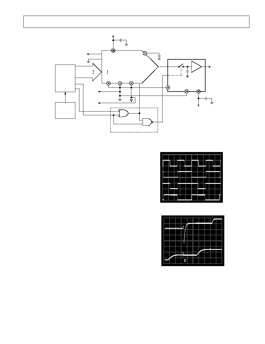
D/A CONVERTER DEGLITCHER
Most D/A converters output an appreciable amount of glitch
energy during a transition from one code to another. The glitch
amplitude can range from several millivolts to hundreds of milli-
volts. This may become unacceptable in many applications. By
selectively delaying the DAC's output transition, the SMP04
can be used to smooth the output waveform. Figure 25 shows
the schematic diagram of such a deglitcher circuit. Two simple
logic gates (an OR and a NAND gate) provide the proper timing
sequence for the DAC
WR strobe and the S/H control signal to
the SMP04. In this example a linear ramp signal is generated by
feeding the most significant eight bits of the 10-bit binary
counter to the DAC. The two least significant bits are used to
produce the delayed
WR strobe and the S/H control signals.
Referring to Figure 26a, new data to the DAC input is set up at
the
S/H's falling edge, but the DAC output does not change
until a
WR strobe goes active. During this period, the SMP04 is
in a sample mode whose output tracks the DAC output. When
S/H goes HIGH, the current DAC output voltage is held by the
SMP04. After 1.2
µ
s settling, the
WR strobe goes LOW to allow
the DAC output to change. Any glitch that occurs at the DAC
output is effectively blocked by the SMP04. As soon as the
WR
strobe goes HIGH, the digital data is latched; at the same time
the
S/H goes LOW, allowing the SMP04 to track to the new
DAC output voltage.
Figure 26b shows the deglitching operation. The top trace
shows the DAC output during a transition, while the bottom
trace shows the deglitched output of the SMP04.
1/4 SMP04
10-BIT
COUNTER
CLOCK
GENERATOR
DB
2
DB
9
DB
0
DEGLITCH LOGIC
1/4 AD7432
1/4 AD7400
A
1
A
0
V
DD
V
REF
OUT
DAC C
OUT
1/4 DAC8426
V
SS
AGND
DGND
WR
+5V
+15V
1 F
AGND
0.1 F
0.1 F1 F CERAMIC
V
OUT
+15V
DGND
S
/H
DB
9
DB
2
V
DD
V
SS
LSB
MSB
V
IN
DIGITAL
RETURN
ANALOG
RETURN
DB
1
Figure 25. DAC Deglitcher
1 s
5V
DB
0
DB
1
WR
S
/H
a.
1 s
50m
DLY
627.4
s
b.
Figure 26. (a) Shows the Logic Timing of the Deglitcher.
The Top Two Traces Are the Two Least Significant Bits,
DB
0
and DB
1
, Respectively. These Are Used to Generate
the
WR and S/H Signals Which Are Shown in the Bottom
Two Traces. (b) Shows the Typical Glitch Amplitude of a
DAC (Top Trace) and the Deglitched Output of the AMP04
(Bottom Trace).
14
SMP04
REV. D
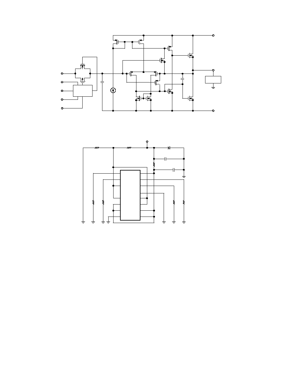
LOAD
V
OUT
N-CH
P-CH
V
IN
V
DD
S
/H
V
SS
DGND
LOGIC
V
DD
V
SS
C
H
Figure 27. Simplified Schematic of One Channel
R2
10k
SMP04
1
2
3
5
6
7
8
9
10
11
12
13
14
15
16
R4
1k
R2
10k
D
1
V
DD
+15V
R2
10k
R2
10k
+
R3
4k
R1
10
C1
10 F
C2
1 F
Figure 28. Burn-In Circuit
SMP04
15
REV. D
OUTLINE DIMENSIONS
Dimensions shown in inches and (mm).
16-Lead Cerdip
(Q-16)
16
1
8
9
0.310 (7.87)
0.220 (5.59)
PIN 1
0.005 (0.13) MIN
0.080 (2.03) MAX
SEATING
PLANE
0.023 (0.58)
0.014 (0.36)
0.200 (5.08)
MAX
0.840 (21.34) MAX
0.150
(3.81)
MIN
0.070 (1.78)
0.030 (0.76)
0.200 (5.08)
0.125 (3.18)
0.100
(2.54)
BSC
0.060 (1.52)
0.015 (0.38)
15°
0°
0.320 (8.13)
0.290 (7.37)
0.015 (0.38)
0.008 (0.20)
16-Lead Plastic DIP
(N-16)
16
1
8
9
0.840 (21.34)
0.745 (18.92)
0.280 (7.11)
0.240 (6.10)
PIN 1
SEATING
PLANE
0.022 (0.558)
0.014 (0.356)
0.060 (1.52)
0.015 (0.38)
0.210 (5.33)
MAX
0.130
(3.30)
MIN
0.070 (1.77)
0.045 (1.15)
0.100
(2.54)
BSC
0.160 (4.06)
0.115 (2.93)
0.325 (8.26)
0.300 (7.62)
0.015 (0.381)
0.008 (0.204)
0.195 (4.95)
0.115 (2.93)
16-Lead SO
(R-16A)
16
9
8
1
0.3937 (10.00)
0.3859 (9.80)
0.2440 (6.20)
0.2284 (5.80)
0.1574 (4.00)
0.1497 (3.80)
PIN 1
SEATING
PLANE
0.0098 (0.25)
0.0040 (0.10)
0.0192 (0.49)
0.0138 (0.35)
0.0688 (1.75)
0.0532 (1.35)
0.0500
(1.27)
BSC
0.0099 (0.25)
0.0075 (0.19)
0.0500 (1.27)
0.0160 (0.41)
8°
0°
0.0196 (0.50)
0.0099 (0.25)
x 45°
PRINTED IN U.S.A.
C313104/98