 | ÐлекÑÑоннÑй компоненÑ: SSM2000 | СкаÑаÑÑ:  PDF PDF  ZIP ZIP |
Äîêóìåíòàöèÿ è îïèñàíèÿ www.docs.chipfind.ru
REV. 0
Information furnished by Analog Devices is believed to be accurate and
reliable. However, no responsibility is assumed by Analog Devices for its
use, nor for any infringements of patents or other rights of third parties
which may result from its use. No license is granted by implication or
otherwise under any patent or patent rights of Analog Devices. (See page 16.)
a
HUSH Stereo Noise Reduction System
with Adaptive Threshold
SSM2000
© Analog Devices, Inc., 1996
One Technology Way, P.O. Box 9106, Norwood, MA 02062-9106, U.S.A.
Tel: 617/329-4700
Fax: 617/326-8703
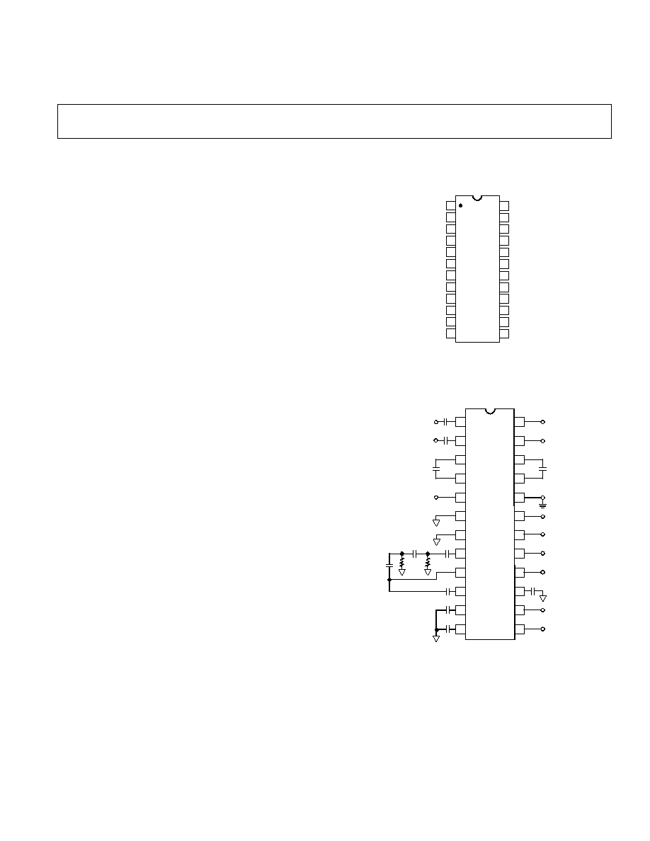
PIN CONFIGURATION
24-Lead Plastic DIP
24-Lead SOIC
13
16
15
14
24
23
22
21
20
19
18
17
12
11
10
9
8
1
2
3
4
7
6
5
TOP VIEW
(Not to Scale)
NC = NO CONNECT
L IN
R VCF C2
R VCF C1
R OUT
L OUT
R IN
L VCF C1
L VCF C2
NC
DIGITAL GND
V
V+
ACOM
VCA PORT
VCF DET IN
SUM OUT
VCA DET IN
AUTO THRESHOLD CAP
DEFEAT
MUTE
VCF DET CAP
VCA DET CAP
DEFAULT THRESHOLD
NC
SSM2000
FEATURES
Up to 25 dB of Noise Reduction from Virtually Any
Audio Source without Sonic Artifacts
"Single-Ended" Operation Eliminates Need for Encode-
Decode Process
Adaptive Threshold Dynamically Adjusts to Changing
Nominal Signal Levels
Effectively Decodes Dolby B
®
Encoded Sources
Direct VCA Control Port Access for Additional Level
Control Functionality
Logic-Controllable Bypass and Muting
100 dB Dynamic Range (Noise Reduction OFF)
0.02% Typical THD+N (@ 1 kHz, Noise Reduction OFF)
+7 V to +18 V Operation
No Royalty Requirements
APPLICATIONS
Auto Radio Sound Processing
Multimedia PC Sound Cards
Television Sound Processing
Cassette Tape Players
AM/FM Receivers
Telephone & Wireless Links
Professional Audio
13
16
15
14
19
18
17
24
23
22
21
20
12
11
10
9
8
1
2
3
4
7
6
5
L IN
R VCF CAP 2
R VCF CAP 1
R OUT
L OUT
R IN
L VCF CAP 1
L VCF CAP 2
DO NOT CONNECT
1
DIGITAL GND
V
V+
ANALOG COMMON (V+/2)
VCA CONTROL PORT
VCF DET IN
SUM OUT
VCA DET IN
AUTO
THRESHOLD CAP
DEFEAT
MUTE
VCF DET TC
VCA DET TC
DEFAULT
THRESHOLD
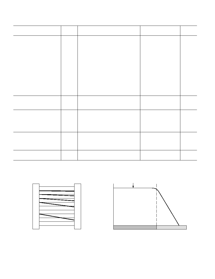
2
1k
2nF
500
20nF
3µF
20nF
1.0µF
3.3µF
6.8µF
6.8µF
1nF
0.22µF
DO NOT CONNECT
1
NOTES:
1
MAKE NO CONNECTION TO PINS 13 AND 18
2
DEFAULT THRESHOLD. NORMALLY CONNECTED TO ANALOG COMMON
1nF
SSM2000
Figure 1. Typical Basic Application
GENERAL DESCRIPTION
The SSM2000 is an advanced audio noise reduction system
based on proprietary HUSH
®
circuitry. HUSH combines a dy-
namic filter and downward expander to provide a high level of
effectiveness without the sonic artifacts normally associated with
noise reduction systems. In addition, an Adaptive Threshold
circuit detects nominal signal levels and dynamically adjusts
both thresholds, thereby providing optimal results regardless of
program source. Since it is a single-ended system, HUSH can
be used on virtually any audio source, including audio and
video tapes, radio and television broadcasts, or any other source
with objectionable noise. The SSM2000 can be used with
Dolby B
encoded sources with excellent results. A key feature is
direct access to the Voltage Controlled Amplifier port enabling
additional functions such as dc volume control, automatic level-
ing, compression, etc. with minimal external circuitry.
Dolby B is a registered trademark of Dolby Laboratories, Inc.
HUSH is a registered trademark of Rocktron Corporation.
REV. 0
2
SSM2000
Parameter
Symbol
Conditions
Min
Typ
Max
Units
AUDIO SIGNAL PATH
Signal-to-Noise Ratio
SNR
V
IN
= 0 V, 20 Hz to 20 kHz (Flat)
80
86
dB
Headroom
HR
Clip Point, THD = 1%
4.5
dBu
Dynamic Range
Clipping to Noise Floor
91
dB
Total Harmonic Distortion
THD+N
V
IN
= 300 mV rms, 2nd & 3rd Harmonics
1
0.02
0.04
%
Effective Noise Reduction
20 kHz Bandwidth (Flat)
Downward Expander Section
15
dB
Dynamic Filter Section
10
dB
Input Impedance
Z
IN
Pins 1 and 2
6
8
k
Output Impedance, Dynamic
Z
OUT
Pins 23 and 24
7
Capacitive Load
No Oscillation
300
pF
Channel Separation
f = 1 kHz, V
IN
= 300 mV
rms
60
dB
Mute Output
V
IN
= 300 mV rms
85
dB
Gain Matching, L & R Channels
VCA at A
V
= 0 dB
±
1
dB
Gain Bandwidth
GBW
NR Disabled
37
kHz
DYNAMIC FILTER
Minimum Bandwidth
BW
MIN
VCF C = 0.001
µ
F
3
kHz
Maximum Bandwidth
BW
MAX
37
kHz
VCA CONTROL PORT
Input Impedance
Pin 7
3.8
k
VCA Voltage Gain Range
A
V
V
IN
= 300 mV rms (Pin 7 = 2.0 V & 0 V)
70
+1
dB
Gain Constant
20
22
26
mV/dB
Control Feedthrough
Pin 7
1
10
mV
POWER SUPPLY
Voltage Range
V
S
+7.0
18
V
Supply Current
I
SY
7.5
11
mA
Power Supply Rejection
PSRR+
70
dB
VCA, VCF DETECTOR
Input Impedance
R
IN
Pins 8 and 10
4.0
5.4
7.0
k
NOTES
1
NR in defeat mode.
Specifications subject to change without notice.
SSM2000SPECIFICATIONS
(V
S
= +8.5 V, ACOM = V
S
/2, f = 1 kHz, R
L
= 100 k
, 0 dBu = 0.775 V
rms.
T
A
= +25 C, Noise Reduction and Adaptive Threshold enabled (Pin 14 at V
S
/2), unless otherwise noted.)
MASKED NOISE
FILTERED NOISE
AUDIO
SIGNAL
6 dB/OCTAVE SLOPE
f
C
= 3 kHz TO 37 kHz
PASSBAND FREQUENCY
RESPONSE
±
0.5 dB
Figure 3. Dynamic Filter Characteristic (For C
F
= 0.001
µ
F
Defeat Mode)
0
10
20
30
40
50
60
70
80
90
100
0
10
20
30
40
50
60
70
80
90
100
INPUT
LEVEL
OUTPUT
LEVEL
Figure 2. Downward Expander Attenuation Characteristic
(In dBt; 0 dBt = Threshold)
SSM2000
REV. 0
3
PIN DESCRIPTION
Pin #
Name
Function and Explanation
1
L IN
Left Audio Input.
2
R IN
Right Audio Input.
3
L VCF C1
Left VCF Filter Cap Port.
4
L VCF C2
Left VCF Filter Cap Port.
5
V+
Positive Supply.
6
ACOM
Analog Common Voltage. In-
ternal Circuit Ground Point.
Must be held to a voltage ap-
proximately halfway between
V+ and V. Should be a clean
low impedance voltage source
capable of at least 4 mA, such
as from a buffer driven off a
supply-splitting voltage divider.
7
VCA PORT
Input to VCA Control Port.
Allows external adjustment of
attenuation with a +22 mV/dB
slope. Zero volts relative to
ACOM gives zero additional
attenuation. Should be con-
nected to ACOM if function
not required.
8
VCF DET IN
Input to VCF Detector.
9
SUM OUT
Combined Left Plus Right
Output.
10
VCA DET IN
Input to VCA Detector.
11
VCF DET CAP
Voltage Controlled Filter.
Time Constant Capacitor Port.
12
VCA DET CAP
Voltage Controlled Amplifier.
Time Constant Capacitor Port.
WARNING!
ESD SENSITIVE DEVICE
CAUTION
ESD (electrostatic discharge) sensitive device. Electrostatic charges as high as 4000 V readily
accumulate on the human body and test equipment and can discharge without detection.
Although the SSM2000 features proprietary ESD protection circuitry, permanent damage may
occur on devices subjected to high energy electrostatic discharges. Therefore, proper ESD
precautions are recommended to avoid performance degradation or loss of functionality.
ABSOLUTE MAXIMUM RATINGS
Supply Voltage . . . . . . . . . . . . . . . . . . . . . . . . . . . . . . . . +18 V
Audio Input Voltage . . . . . . . . . . . . . . . . . . Supply Voltage(s)
Control Port Voltage (Pin 7) . . . . . . . . . . . . . . Positive Supply
Default Override (Pin 14) . . . . . . . . . . . . . . . . . . . . . . . . . V+
Defeat (Pin 16) . . . . . . . . . . . . . . . . . . . . . . . . . . . . . . . . . V+
Mute Override (Pin 17) . . . . . . . . . . . . . . . . . . . . . . . . . . . V+
Operating Temperature Range . . . . . . . . . . . . 40
°
C to +85
°
C
Storage Temperature Range . . . . . . . . . . . . 65
°
C to +150
°
C
Junction Temperature (T
J
) . . . . . . . . . . . . . . . . . . . . . +150
°
C
Lead Temperature (Soldering, 60 sec) . . . . . . . . . . . . . +300
°
C
ESD RATINGS
883 (Human Body) Model . . . . . . . . . . . . . . . . . . . . . . 2.5 kV
EIAJ Model . . . . . . . . . . . . . . . . . . . . . . . . . . . . . . . . . . 300 V
ORDERING GUIDE
Temperature
Package
Package
Model
Range
Description
Option
SSM2000P
40
°
C to +85
°
C
24-Pin Plastic DIP
N-24
SSM2000S
40
°
C to +85
°
C
24-Pin SOIC
SOL-24
PACKAGE INFORMATION
Package Type
JA
1
JC
Units
24-Pin Plastic DIP (P)
54
27
°
C/W
24-Pin SOIC (S)
72
24
°
C/W
NOTE
1
JA
is specified for the worst case conditions, i.e.,
JA
is specified for device in socket
for P-DIP packages;
JA
is specified for device soldered onto a circuit board for
surface mount packages..
Pin #
Name
Function and Explanation
13
NC
Make No Connection to this
Pin.
14
DEFAULT
Default Threshold Adjust-
THRESHOLD
ment Port. Allows reduction
of noise reduction action if
signal source is relatively
clean such as CD sources.
Normally connected to Analog
Common. 1.2 V is recom-
mended for CDs; 2 V com-
pletely defeats noise reduction.
15
AUTO THRESHOLD
CAP
Automatic Threshold Detec-
tor Capacitor Port.
16
DEFEAT
Logic High: Defeats Noise
Reduction.
Logic Low: Normal Action.
Connect to Ground if not used.
17
MUTE
Logic High: Mute.
Logic Low: Normal Action.
Connect to Ground if not used.
18
NC
Make no connection to this
pin.
19
DIGITAL GND
Digital Logic Reference
(Logic Zero).
20
V
Negative Supply.
21
R VCF C2
Right VCF Capacitor Port.
22
R VCF C1
Right VCF Capacitor Port.
23
R OUT
Right Audio Output.
24
L OUT
Left Audio Output.
SSM2000
REV. 0
4
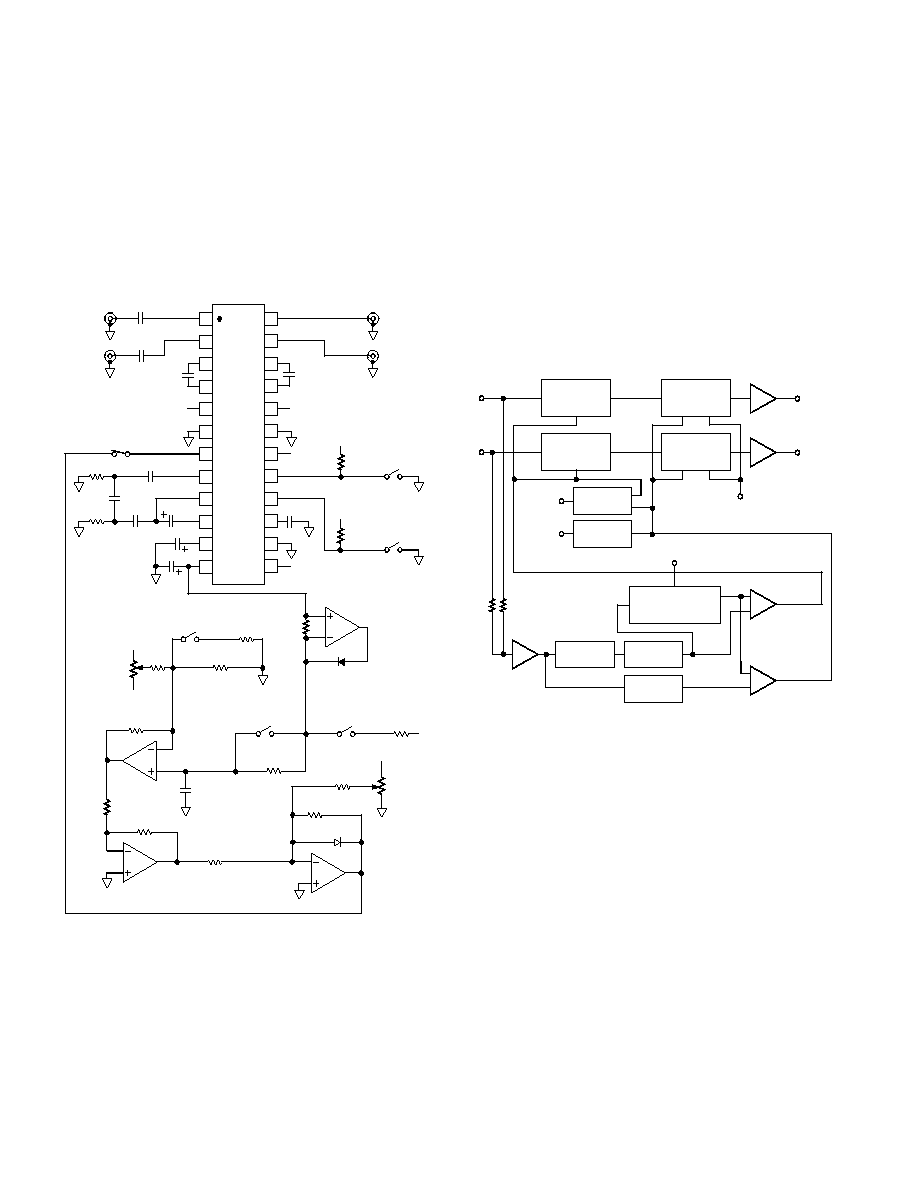
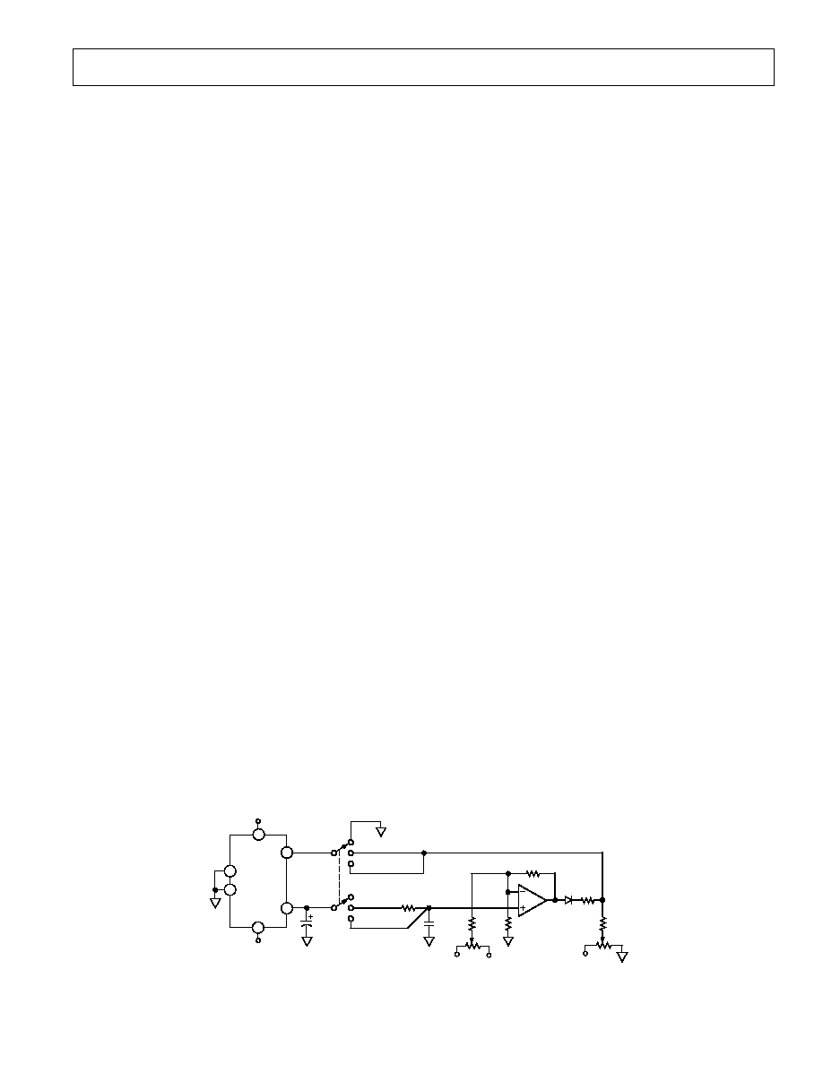
APPLICATIONS
This applications example (Figure 4) demonstrates some of the
additional functions that can be easily implemented through use
of the VCA Control Port (Pin 7). These functions can be selected
to operate simultaneously with the basic HUSH noise reduction
function. The VCA detector output provides a signal which can
be further processed using one quad op amp (OP482) to provide
these various additional useful functions.
The circuit shown in the figure below achieves: (1) Compres-
sion, (2) Volume Leveling, (3) DC Volume Adjustment.
C3
0.001µF
C10
0.001µF
NC
C2
6.8µF
+5V
5V
C1
6.8µF
C4
0.0022µF
12
11
10
9
8
1
2
3
4
7
6
5
13
16
15
14
19
18
17
24
23
22
21
20
SSM2000
C7
2.2µF
C6
0.022µF
10%
JA1
RCA
LEFT IN
JA2
RCA
RIGHT IN
C5
0.022µF
R1
1k
NC
C8
1µF
C9
3.3µF
R2
510
+5V
R3
3k
SW1-C
MUTE
OPEN = MUTE
CLOSED = OFF
C11
0.22µF
+5V
R4
3k
SW1-B
BYPASS
OPEN = BYPASS
CLOSED = HUSH
SW1-F
SIDE CHAIN
OPEN = OUT
CLOSED = IN
JA3
RCA
LEFT OUT
JA4
RCA
RIGHT OUT
R16
1.5M
U1-A
OP482
3
2
1
1N4148
SW1-E
OPEN = LEVEL
CLOSED = COMP
R15
10M
SW1-A
OPEN = COMP
CLOSED = LEVEL
R9
7.5k
R10
5.1k
R8
20k
+5V
5V
LEVEL
THRESHOLD
R7, 10k
PT10V
U1-D
OP482
13
12
14
R11
12k
SW1-D
OPEN = LEVEL
CLOSED = COMP
R14
100k
5V
C12
1µF NON-POLARIZED
10% POLY, 63V
R12
20k
9
10
8
R13
20k
U1-C
OP482
R17
20k
U1-B
OP482
6
5
7
D2
1N4148
R19
20k
5V
VOLUME
CONTROL
VR1, 10k
LINEAR
R18
30k
Figure 4. Typical Dual Supply Application and Test Circuit
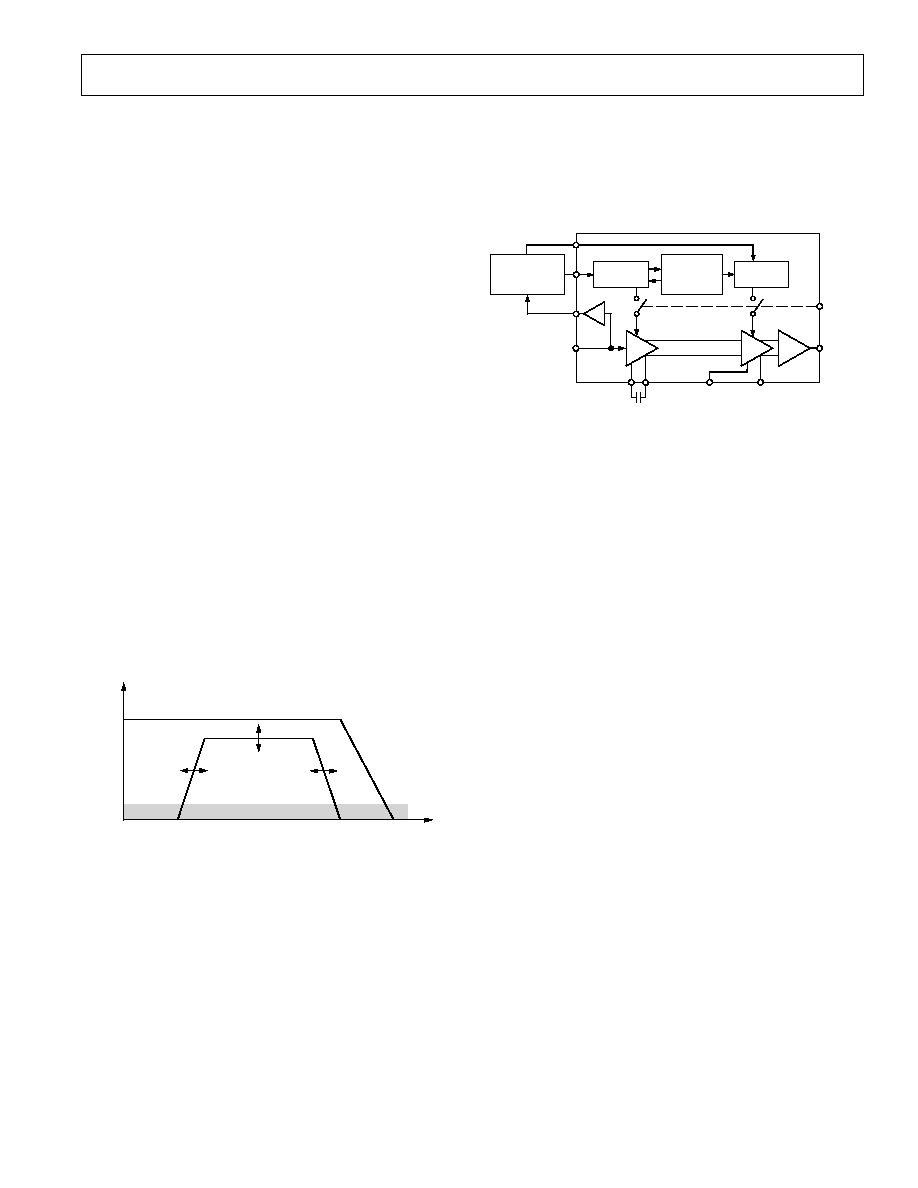
SIMPLIFIED THEORY OF OPERATION
The input audio signals are processed to extract information
concerning the frequency distribution and amplitude of both
the desired signals and the undesired noise. Left and right au-
dio signals are passed through voltage controlled (low-pass) fil-
ter, and then through a voltage controlled amplifiers. Both the
filters and amplifiers are low distortion, and add negligible noise
of their own. The VCF has a user-definable cutoff range that is
usually set from 1 kHz to 35 kHz. It can be set to cover other
ranges as required by the application. The VCA can be adjusted
from a loss to a gain, adding to the SSM2000's versatility. In
accordance with proprietary patented algorithms, control sig-
nals are derived and applied to both the VCF and VCA, result-
ing in up to 25 dB noise suppression with the minimum loss of
desired signals.
DEFEAT
EXTERNAL VCA
CONTROL PORT
R
OUT
L
OUT
R
IN
L
IN
DEFAULT
THRESHOLD
VOLTAGE
CONTROLLED
FILTER
VOLTAGE
CONTROLLED
AMPLIFIER
LOGIC
INTERFACE
VOLTAGE
CONTROLLED
FILTER
VOLTAGE
CONTROLLED
AMPLIFIER
MUTE
LOGIC
INTERFACE
DIFFERENCE
AMPLIFIER
AUTO THRESHOLD
NEGATIVE PEAK
DETECTOR
HIGH-PASS
FILTER
PEAK
DETECTOR
PEAK
DETECTOR
DIFFERENCE
AMPLIFIER
Figure 5. SSM2000 System Block Diagram
INPUT SIGNAL V
rms
10
1
0.01
0.01
2
0.1
THD + N %
1
0.1
T
A
= +25
°
C
V
S
=
±
4.25V (Pin 5, 20)
DEF THRESHOLD = 0V (Pin 14)
DEFEAT = ON (Pin 16)
MUTE = OFF (Pin 17)
R
L
= 100k
BOTH CHANNELS
Figure 6. THD+N (%) vs. Input Signal
FREQUENCY Hz
1
0.1
0.001
20
30k
100
THD + N %
1k
10k
0.01
T
A
= +25
°
C
V
S
=
±
4.25V (Pin 5, 20)
V
IN
= 300mV
rms
SINE WAVE (Pin 1, 2)
DEF THRESHOLD = 0V (Pin 14)
DEFEAT = ON (Pin 16)
MUTE = OFF (Pin 17)
R
L
= 100k
BOTH CHANNELS
Figure 7. THD+N (%) vs. Frequency
FREQUENCY Hz
6
4
12
20
200k
100
GAIN dB
1k
10k
100k
2
0
8
2
4
6
10
T
A
= +25
°
C
V
S
=
±
4.25V (Pin 5, 20)
V
IN
= 300mV
rms
SINE WAVE (Pin 1, 2)
DEF THRESHOLD = 0V (Pin 14)
DEFEAT = ON (Pin 16)
MUTE = OFF (Pin 17)
R
L
= 100k
BOTH CHANNELS
Figure 8. 3 dB Bandwidth
INPUT SIGNAL dBu
@ 1kHz
0
100
70
0
60
OUTPUT SIGNAL dBu
50
40
30
20
10
10
60
70
80
90
30
50
20
40
V
TH
= 0V
V
TH
= 1.2V
V
TH
= 2.0V
T
A
= +25
°
C
V
S
=
±
4.25V (Pin 5, 20)
DEF THRESHOLD = 0V (Pin 14)
DEFEAT = OFF (Pin 16)
MUTE = OFF (Pin 17)
R
L
= 100k
0dBu = 0.775mV
rms
Figure 9. Output vs. Input Characteristics (With Different
Adaptive Threshold Voltage, Pin 17)
VCA CONTROL VOLTAGE (Pin 7) V
10
90
1
3
0.5
L, R CHANNEL OUTPUT dB
0
0.5
1
1.5
2
2.5
0
30
50
70
80
10
20
40
60
T
A
= +25
°
C
V
S
=
±
4.25V (Pin 5, 20)
V
IN
= 300mV
rms
SINE WAVE (Pin 1, 2)
DEF THRESHOLD = 0V (Pin 14)
DEFEAT = OFF (Pin 16)
MUTE = OFF (Pin 17)
R
L
= 100k
BOTH CHANNELS
Figure 10a. Channel Output vs. VCA Control Voltage (Pin 7)
FREQUENCY Hz
20
80k
100
GAIN dB
1k
10k
3.00
0.7
20.0
1.6
3.9
6.2
8.5
10.8
13.1
15.4
17.7
T
A
= +25
°
C
V
S
=
±
4.25V (Pin 5, 20)
V
IN
= 300mV
rms
SINE WAVE (Pin 1, 2)
DEF THRESHOLD = 0V (Pin 14)
DEFEAT = OFF (Pin 16)
MUTE = OFF (Pin 17)
R
L
= 100k
100 2kHz MIN BW
4kHz
6kHz
8kHz
20kHz
40kHz
50kHz
Figure 10b. VFC Characteristics (Simulated Noise Level
90 mV rms with Different Frequency) Applied through a
3-Pole HP filter
Typical Performance CharacteristicsSSM2000
5
REV. 0
FREQUENCY Hz
20
30k
100
1k
10k
10
0
90
10
20
30
40
50
60
70
80
CHANNEL OUTPUT dB
T
A
= +25
°
C
V
S
=
±
4.25V (Pin 5, 20)
V
IN
= 300mV
rms
SINE WAVE (Pin 1, 2)
V
C
= 0V
V
C
= 0.5V
V
C
= 1V
V
C
= 1.5V
V
C
= 2V
V
C
= 2.5V
DEF THRESHOLD = 0V (Pin 14)
DEFEAT = OFF (Pin 16)
MUTE = OFF (Pin 17)
R
L
= 100k
Figure 11. Channel Output vs. Frequency for Different
VCA Control Port Voltages
FREQUENCY Hz
40
45
70
20
20k
100
1k
10k
50
55
60
65
CHANNEL SEPARATION dB
T
A
= +25
°
C
V
S
=
±
4.25V (Pin 5, 20)
DEF THRESHOLD = 0V (Pin 14)
DEFEAT = ON (Pin 16)
MUTE = OFF (Pin 17)
R
L
= 100k
V
IN
= 300mV
rms
SINE WAVE (Pin 1 or 2)
UNSELECTED INPUT = 0V (Pin 1 or 2)
Figure 12. Channel Separation vs. Frequency
FREQUENCY Hz
50
55
100
20
30k
100
MUTED OUTPUT LEVEL dB
1k
10k
60
65
70
75
80
85
90
95
T
A
= +25
°
C
V
S
=
±
4.25V (Pin 5, 20)
V
IN
= 300mV
rms
SINE WAVE (Pin 1, 2)
DEF THRESHOLD = 0V (Pin 14)
DEFEAT = OFF (Pin 16)
MUTE = ON (Pin 17)
BOTH CHANNELS
R
L
= 100k
Figure 13. Muted Output Level vs. Frequency
FREQUENCY Hz
20
30
80
20
30k
100
PSRR
+
dB
1k
10k
40
50
60
70
T
A
= +25
°
C
V
S
=
±
4.25V (Pin 5, 20)
DEF THRESHOLD = 0V (Pin 14)
DEFEAT = ON (Pin 16)
MUTE = OFF (Pin 17)
NO DECOUPLING CAPACITOR ON V
+
V
+
RIPPLE = 425mV
p - p
Figure 14. PSRR+ vs. Frequency
FREQUENCY Hz
20
30
80
20
30k
100
1k
10k
40
50
60
70
PSRR
dB
T
A
= +25
°
C
V
S
=
±
4.25V (Pin 5, 20)
DEF THRESHOLD = 0V (Pin 14)
DEFEAT = ON (Pin 16)
MUTE = OFF (Pin 17)
V
RIPPLE = 425mV
p - p
NO DECOUPLING CAPACITOR ON V
Figure 15. PSRR vs. Frequency
SUPPLY VOLTAGE V
14
4
4
20
6
SUPPLY CURRENT mA
8
10
12
14
16
18
13
10
8
6
5
12
11
9
7
T
A
= +25
°
C
Figure 16. Supply Current vs. Supply Voltage
SSM2000Typical Performance Characteristics
6
REV. 0
SSM2000
REV. 0
7
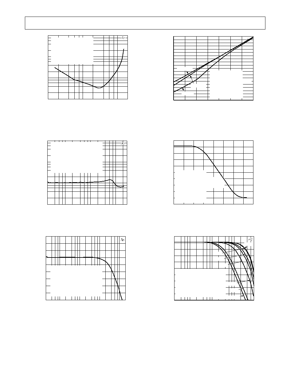
APPLICATIONS INFORMATION
Introduction
The SSM2000 is a dual channel audio noise reduction IC which
reduces noise through a combination of variable filtering and
downward expansion in conjunction with a unique adaptive
noise threshold detector. These two techniques yield an overall
noise reduction of up to 25 dB on AM and FM radio, open reel
and cassette tape, CD, Dolby B encoded programming, broad-
cast studio-transmitter links, telephone lines, and other audio
sources without the need for any additional manual adjustment.
The HUSH Noise Reduction System as implemented in the
SSM2000 has been shown to substantially reduce noise in PC
multimedia, intercom systems, teleconferencing systems, mobile
communications, automotive audio, home stereos and televi-
sions, and other consumer and professional audio applications
while preserving full signal fidelity and transparency.
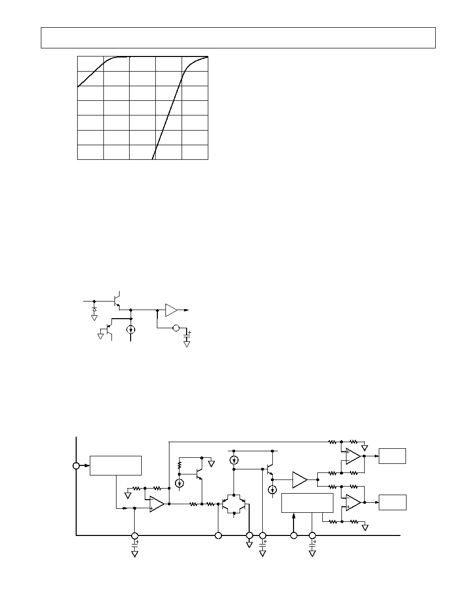
A brief explanation of the nature of audio signals is useful before
discussing the details of the SSM2000's operation. First, audio
signals have both amplitude and frequency content. Music and
voice are created by changing both the amplitude and frequency
of sound waves as shown in Figure 17. Second, the highest
audio signal amplitudes typically occur at low frequencies
(100 Hz1 kHz) and taper off exponentially as frequency in-
creases. Third, when an audio signal is recorded, audio noise is
also generated. This noise is the white noise "hiss" or waterfall
sound that is easily heard on taped material. Audio noise for a
given source and bandwidth does not, in general, change with
frequency or amplitude. However, noise levels do change be-
tween different sources, because of differences in recording
equipment, media, and the surrounding environment. Fourth,
psychoacoustic effects mask noise that occurs at or near the fre-
quency of the audio signal. Finally, audio noise is usually con-
sidered to be most objectionable in the 3 kHz8 kHz bandwidth
region.
NOISE
MUSIC'S
FREQUENCY
AND AMPLITUDE
ENVELOPE
NORMAL AUDIO SYSTEM FREQUENCY
AND AMPLITUDE ENVELOPE
AMPLITUDE
FREQUENCY
Figure 17. A Frequency-Amplitude Plot of the Audio
Envelope
An analog noise reduction system must first distinguish between
the desired source material and the undesirable noise. It must
then attenuate the noise while leaving the source material unaf-
fected. One approach to noise reduction is to assume that signal
below a predetermined amplitude is noise, and to then attenuate
the noise by using a Voltage Controlled Amplifier (VCA). A
variation of this noise reduction method is found in Dolby B
cassette tape systems. This method achieves about 10 dB of
improvement in signal-to-noise ratio (SNR). This system incor-
porates a high-frequency compressor on the recording side, and
a high frequency expander during playback. Another noise
reduction technique senses and reduces noise by measuring the
frequency content of the audio signal and then filters noise that
occurs above the highest signal frequency. This noise reduction
method utilizes a Voltage Controlled Filter (VCF) and is the
basic method of operation in the DNR
®
system, which provides
about 10 dB of noise reduction. The HUSH system shown in
Figure 34 combines elements of both of these techniques to
achieve 25 dB of noise reduction, and also has significant
improvements.
x3
PRE-DETECTOR
SIGNAL
CONDITIONING
VCF
DETECTOR
NOISE
THRESHOLD
DETECTOR
SSM2000
VCA
DETECTOR
L/R IN
L/R OUT
VCA EXTERNAL
CONTROL
PORT
MUTE
VCF FILTER
CAP
HUSH
DEFEAT
1,2
3,22
4,21
7
17
24,23
16
OUT
AMP
8
9
10
VCF
VCA
Figure 18. SSM2000 Block Diagram (One Audio Channel
Shown)
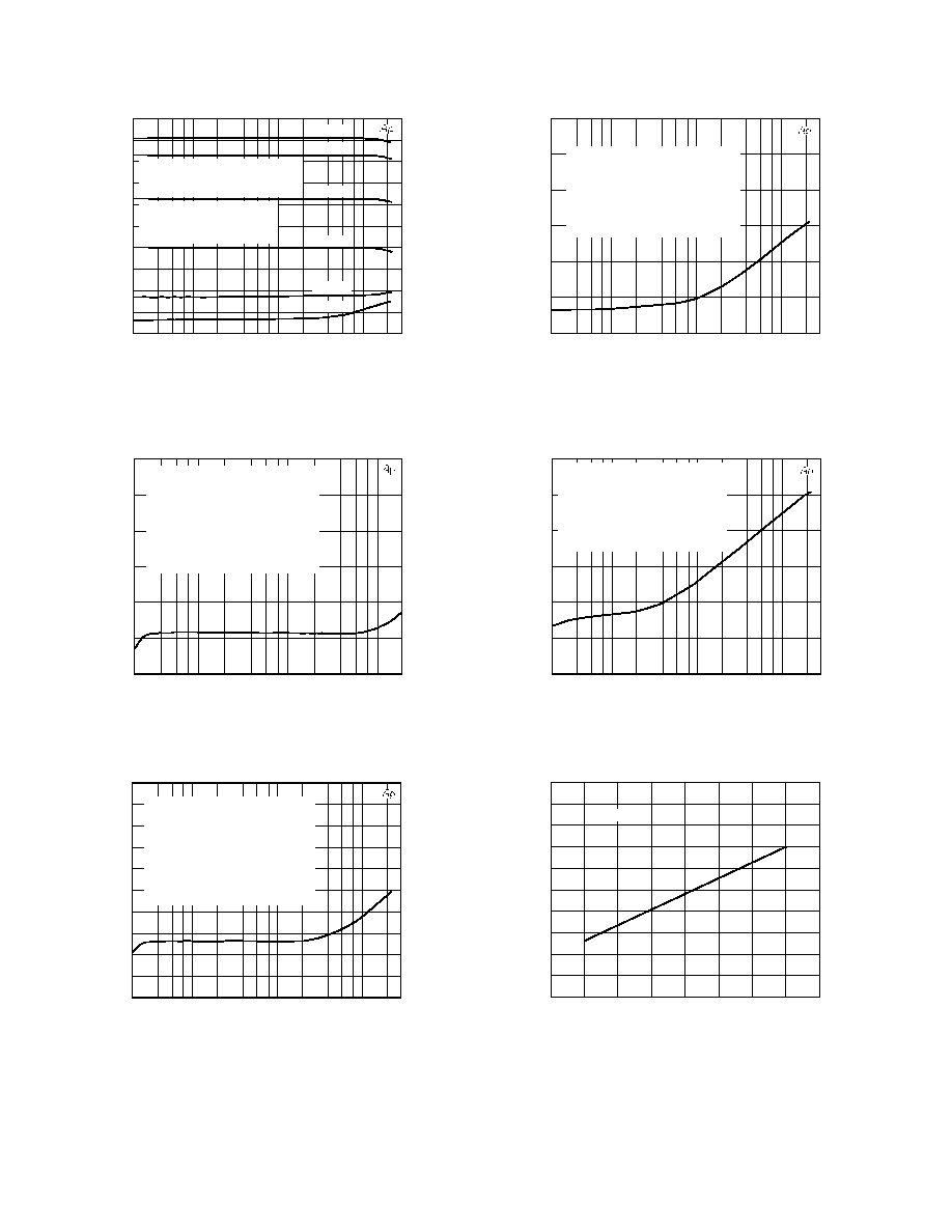
Recalling that the noise floor changes with different audio
sources due to recording equipment, media, and the environ-
ment, we realize that fixed threshold approaches cannot yield
optimal results. The HUSH Noise Reduction System incorpo-
rates an automatic noise threshold detector that senses these
changes and adapts the VCA and VCF to become more or less
aggressive depending on the amplitude of the noise floor. To
determine the amplitude of the noise floor the SSM2000 as-
sumes that the averaged amplitude during short periods of no
audio is equal to the noise floor. This assumption works well in
audio applications, but does have implications for evaluation
and testing that are discussed in the "Evaluating the SSM2000"
section.
Variable Low-Pass Filtering
The audio signal is first passed through a single-pole low-pass
Voltage Controlled Filter (VCF). Both the Left and Right
VCFs are controlled by a detector which places their cutoff fre-
quencies just beyond the highest audio signal frequency. Since
the highest audio signal frequency constantly changes, the
VCF's cutoff frequency must also change in concert with the
audio signal to avoid attenuating desired signal.
For example, with signal levels below the filter threshold (pre-
sumed to be mostly noise), the VCF shuts down to about 1 kHz,
providing noise reduction in the critical 3 kHz 8 kHz band, as
Figure 19 illustrates. The VCF progressively "opens up" as
higher frequency amplitudes are detected at the inputs. The
VCF's cutoff reaches 20 kHz when the high frequency signal
amplitude is 30 dB above the threshold. At this point the VCF
is acoustically transparent. The VCF's cutoff frequency range is
between 1 kHz to 35 kHz. The minimum range of the VCF is
limited to 1 kHz for two reasons: one, to avoid high frequency
loss at the leading edge of transients, because the lower the
minimum cutoff the longer it takes the VCF to slew "open," and
two, noise is most objectionable at mid and high range frequen-
cies. Once again, if the VCF characteristics are to be measured,
then please refer to the section on "Evaluating the SSM2000."
DNR is a registered trademark of National Semiconductor Corporation.
SSM2000
REV. 0
8
MASKED NOISE
AUDIO
SIGNAL
BYPASS FREQUENCY RESPONSE
±
0.5 dB
AMPLITUDE
FREQUENCY
fc = 1kHz to 35kHz
6dB/OCTAVE
SLOPE
FILTERED NOISE
Figure 19. A Frequency Amplitude Plot Illustrating the
Noise Reducing Effect of the VCF
The SSM2000 has been designed to minimize control feedthrough.
Control feedthrough may cause an audible output as the internal
control lines of the VCAs and VCFs are changed rapidly. This
feedthrough is the cause of many of the unpleasant artifacts
prevalent among noise reduction systems and is often due to
parasitic capacitance and mismatches within the IC. This speci-
fication is important for the VCA and VCF, but the VCF is the
most susceptible because it operates at constant dc gain. The
solution incorporated into the SSM2000 to reduce control feed-
through has been to convert from single-ended to full differen-
tial at the signal input and convert back again at the output
buffer. Because the audio path through the VCA and VCF are
fully differential, control feedthrough is determined purely by
mismatches with no systematic errors. The slight penalty to be
paid for a fully differential system, besides extra complexity, is
that the external VCF capacitors (1 nF recommended) now re-
quire two pins each instead of one. Careful attention to VCF
capacitor matching and layout symmetry reduces control
feedthrough to better than 40 dB through the signal path.
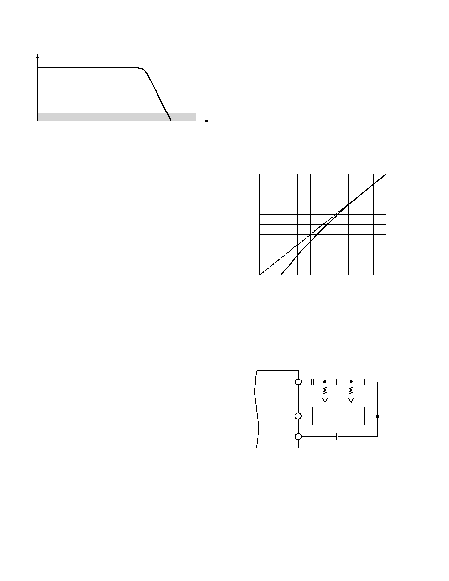
Downward Expander
After the audio signal passes through the VCF, it is then differ-
entially sent to the VCA. The VCA is characterized by a
downward expander transfer function as shown in Figure 20.
Attenuation begins at output levels below the internal threshold
at an effective rate of 2.2 dB/decade. Therefore, audible noise
is attenuated when source material is not present. Conversely,
when audio source levels are at or above the threshold, the VCA
is set to unity gain. Because of well documented psychoacoustic
effects, it is valid to assume that at high audio amplitudes audio
noise is being masked by the audio material. The control infor-
mation that is required for the downward expander to function
properly is provided by the internal VCA detector side-chain cir-
cuitry common to both the L and R channels.
Previous downward expander circuits have often used a higher
ratio than 2.2 dB/decade to provide impressive noise reduction
figures (50 dB or more) in the absence of signal information.
However, in most applications, such severe noise gating is to-
tally pointless, and actually exacerbates the effects of VCA con-
trol feedthrough, since control feedthrough is not attenuated as
the VCA shuts down. For this reason, the maximum VCA at-
tenuation in the SSM2000 is limited to 15 dB. In addition, the
"smooth" roll-off of the downward expander eliminates any
audible artifacts resulting from this type of noise reduction. In
contrast, many noise reduction system employ gates and com-
parators that result in dramatic shifts in attenuation. In these
types of noise reduction systems noise can be heard switching in
and out during periods of low volume audio near that attenua-
tion discontinuity. Telephone systems with noise gating are par-
ticularly prone to this type of behavior, because the noise level of
a poor quality connection is very near the gate's switching level.
The Mute function (Pin 17) can override the VCA controls, as
shown in Figure 5. When mute is active (HIGH), it pulls the
VCA to maximum attenuation. An 85 dB professional quality
mute under worse case conditions can be expected over most of
the audible frequency range as shown in Figure 13. Mute over-
rides both the internal VCA control coming from the VCA De-
tector and the external VCA control port (Pin 7). The external
VCA control port is additive in nature to the internal VCA con-
trol signals; therefore, noise reduction and volume control may
occur simultaneously in the SSM2000. The VCA control port
allows the gain of the VCA to changed externally at approxi-
mately 22 mV/dB, where 150 mV is equal to 0 dB, as shown in
Figure 10a.
INPUT IN dB
30
30
70
70
30
60
OUTPUT IN dB
50
40
30
20
10
0
10
20
20
20
40
60
0
10
50
10
Figure 20. Downward Expander Transfer function
VCF Detector
Both the VCF and VCA detectors are amplitude detectors and
identical in every way. The applied input signals to the detec-
tors must be preconditioned for the detector circuitry to give
the information that is required by the L and R VCFs and
VCAs. Figure 21 is a schematic of the recommended precondi-
tioning filters for use with the VCA and VCF detectors.
VCF
DETECTOR
INPUT
SSM2000
SUM OUT
VCA
DETECTOR
INPUT
2.2nF
1k
22nF
510
22nF
ADDITIONAL
FIXED-FREQUENCY
FILTER IF NECESSARY
8
9
10
2.2µF
Figure 21. The Recommended Signal Preconditioning
Filters for the VCA and VCF Detectors
The VCF detector is fed by 3
×
(L+R)/2 averaged input signal
processed by a three-pole high pass filter with a 15 dB point at
10 kHz. In Figure 22, the response of the VCF's 3-pole filter is
shown. The VCF preconditioning filter performs two func-
tions: first, it eliminates the large amplitude, low frequency au-
dio which would otherwise mask the high frequency signals;
and second, it becomes increasingly sensitive throughout most
of the VCF's frequency range of interest (660 Hz to 20 kHz),
compensating for the effect of most audio signals which typi-
cally decrease in amplitude as frequency increases.
SSM2000
REV. 0
9
FREQUENCY Hz
0
10
70
1
100k
10
OUTPUT IN dB
100
1k
10k
30
40
50
60
20
VCA
VCF
Figure 22. Preconditioning Filter Responses for the VCF
DET IN and VCA DET IN
Once the preconditioned VCF signal is applied to the input of
the VCF detector, the log(x) of the signal is taken. This log
function essentially removes the effect of large signal peaks and
smoothes out the response of the VCF control. After the log(x)
is taken the signal is rectified. The signal is rectified for the fol-
lowing two reasons: first, the following peak detector's output
will have less ripple, because twice as many peaks are available;
and second, the most negative potential of the rectified signal is
equivalent to the noise floor. Following the rectifier, the signal
is positive peak detected, as shown in Figure 23.
1.1µA
D1
Q4
Q3
VCF DET CAP
1µF
V
EE
V
EE
TO AUTO
THRESHOLD
AND DIFFERENCE
AMPLIFIER
RECTIFIED
AND LOG (x) OF
VCA DET IN
AND VCF DET IN
11
Figure 23. VCA DET IN and VCF DET IN's Positive Peak
Detector Circuitry
The attack time of the VCF control is set internally and cannot
be decreased, however the release time constant is directly pro-
portional to the value of the capacitor VCF DET CAP. Signals
above the potential at Pin 11 cause the emitter diode of Q3 to
turn on, thus rapidly charging the VCF DET CAP (Pin 11).
When the audio signal has dropped below the potential at VCF
DET CAP, the emitter diode of Q3 is turned off. During this
condition, an internal 1.1
µ
A current source sets the release time
by discharging the VCF DET CAP. The release time constant
of the VCF Detector is about 10 times faster than the release
time constant of the Auto Threshold Detector. This ratio
should not be decreased, because the output of the VCF Detec-
tor is negative peak detected to arrive at the Auto Threshold
level (for more information please refer to the Auto Noise
Threshold section). The output of the VCF detector (Pin 11) is
multiplied by 13 (A1 of Figure 24) and then the noise threshold
is subtracted (A2 of Figure 24) to arrive at the actual control
voltage for the L and R VCFs. D1 and Q4 are used to set limits
on the output of the detector circuitry to ensure that the detec-
tor remains responsive to pulsed high frequency audio.
VCA Detector
The VCF and VCA detectors are identical, therefore refer to the
previous section on the VCF detector for detailed information of
the internal operation of these detectors. The VCA detector is
used to detect the audio-band signal amplitude (20 Hz20 kHz).
Usually the lower frequencies 50 Hz to 2 kHz contain the high-
est audio amplitudes. Therefore, the VCA's preconditioning fil-
ter must allow low frequency signals to be presented to the VCA
detector. A single pole filter is used to accomplished this func-
tion. This filter is formed by a 2.2
µ
F capacitor and the 6 k
of
internal input impedance of Pin 10 as shown in the schematic,
Figure 21.
Adaptive Noise Threshold
The threshold level chosen for both the variable filter and down-
ward expander is of prime importance in differentiating between
signal and noise. In an automotive environment for example,
the audio sources are generally AM and FM radio, tape, and
CD. Setting the noise threshold at a value suitable to improve a
noisy FM station could easily wipe out most of the dynamic
range of a CD. FM station threshold setting is compounded by
the vast variations in signal strength in any given location, and
the fact that many FM receivers will revert to monaural opera-
tion with a greatly improved signal to noise ratio when signal
strengths become weak. It is also unreasonable to expect the
driver of an automobile to fiddle with panel controls in order to
improve the threshold tracking. The patented adaptive noise
threshold in the SSM2000 solves these problems, maintaining
the transparency of the noise reduction system under most op-
eration conditions while not introducing cumbersome end-user
controls.
ATCAP
0.22µF
V
EE
AND FAST
PEAK
DETECTOR
VCF LOG (RECTIFIER)
A3
20k
20k
20k
20k
20k
20k
A2
20k
20k
V
EE
V
CC
20k
20k
V
EE
A1
600
7.2k
DEF
35nA
SSM2000
VCF TC
1µF
VCA TC
3.3µF
VCF
CONTROL
TO VCA
CONTROL
AND FAST
PEAK
DETECTOR + OP AMP
VCA LOG (RECTIFIER)
14
10
12
15
11
13
8
Figure 24. Schematic Diagram of the Adaptive Noise Threshold and Related Circuitry
SSM2000
REV. 0
10
Noise is most objectionable at high frequencies (3 kHz8 kHz).
Therefore, only the VCF detector output signal is used to deter-
mine the adaptive noise threshold. Figures 25ac, are a series of
circuits which illustrate how the noise threshold is derived. It is
important to remember that the signal that is applied to the
noise threshold detector circuitry has already been rectified and
averaged. Hence, the lowest potential over a set period of time
corresponds to the noise floor. Node A corresponds to the out-
put of the VCF Detector, and Node B is
proportional to the adaptive noise threshold.
Figure 25a illustrates the condition where the potential at Node
A is above the maximum possible potential for Node B. The
maximum noise threshold is set by the potential placed on Pin
14. If the potential at Node B rises to a diode drop above Pin
14, then Q1's emitter-base diode turns on and clamps Node B.
This is represented by the current flow I2. However, if Node B
has not yet risen to the maximum noise threshold level, then
both Q1 and Q2 are OFF and the 35 nA current source is
charging C1 (A.T. CAP). The auto threshold capacitor should
be a ceramic or equivalent low leakage capacitor, because the
charging current could otherwise be of similar amplitude to the
capacitor leakage current.
V
EE
A
20k
20k
MAXIMUM
NOISE THRESHOLD
LEVEL
35nA
14
15
Q1
Q2
C1
0.22µF
MINIMUM
NOISE
THRESHOLD
LEVEL
B
I 2
I 1
t
Q1 CLAMPS NODE
B TO A DIODE DROP
ABOVE THE
POTENTIAL AT PIN 14
I1 IS
CHARGING
C1
B
VOLTS
A
MAX
MIN
Figure 25a. Condition Where the Actual Noise Threshold
Is Above the Maximum Noise Threshold Level Setting
(Pin 14)
Figure 25b illustrates the condition where the potential at Node
A is between the maximum and minimum potentials for Node
B. When Node A falls below Node B, then the emitter-base
diode of Q2 turns ON causing Node B to follow Node A. Cur-
rent I2 illustrates how the discharge current from C1 and the
35 nA current source are directed through Q2. Q2 shuts OFF
the moment that Node A rises above Node B. This forces the
35 nA current source to begin charging C1 at a constant rate set
by the value of C1 at Pin 15.
V
EE
A
20k
20k
MAXIMUM
NOISE THRESHOLD
LEVEL
35nA
14
15
Q1
Q2
C1
0.22µF
MINIMUM
NOISE
THRESHOLD
LEVEL
B
t
I2 FLOWS DISCHARGING
C1 CAUSING NODE B TO
VOLTAGE FOLLOW NODE A
I1 IS
CHARGING
C1
B
VOLTS
A
MAX
MIN
I 2
I 1
Figure 25b. Condition Where the Noise Level Is Between
the Maximum and Minimum Threshold Settings
Figure 25c illustrates the condition where the potential at Node
A is below the minimum potential for Node B. In this case the
internal minimum noise potential causes a diode to turn ON.
This clamps the Node A potential to the minimum noise thresh-
old level. I1 represents the current flow in this condition. In
addition, the 35 nA flows through Q2's emitter-base diode as
shown by I2.
V
EE
A
20k
20k
35nA
14
15
Q1
Q2
C1
0.22µF
MINIMUM
NOISE
THRESHOLD
LEVEL
B
C
MAXIMUM
NOISE THRESHOLD
LEVEL
I 2
I 1
t
I 1 AND I 2 FLOW CLAMPING NODE
B TO THE MINIMUM NOISE
THRESHOLD LEVEL
B
VOLTS
A
MAX
MIN
C
Figure 25c. Condition Where the Noise Level Is Below the
Minimum Noise Threshold Level Setting
Simply subtracting the noise threshold from the average VCF
HF control signal plus noise threshold and the average VCA
control signal plus noise threshold will yield the final VCF and
VCA control signal. This operation is accomplished with two
internal difference amplifiers.
Figures 26ab shows the response of the detector that controls
the VCF bandwidth and VCA gain respectively. Both L IN and
R IN pins receive a 10 kHz tone burst. The lower trace of Fig-
ure 26a shows the control voltage to the VCF (Pin 11) and the
lower trace of Figure 26b shows the control voltage to the VCA
(Pin 12). Note the quick rise and slow fall times. This allows
fast adaptation to changed input signal conditions, while avoid-
ing pumping effects and other sonic artifacts.
100
90
10
0%
100mV
100ms
500mV
Figure 26a. VCF Control Voltage for a Tone Burst
100
90
10
0%
500mV
100mV
100ms
Figure 26b. VCA Control Voltage for a Tone Burst
SSM2000
REV. 0
11
SSM2000
V+
V
20
ACOM
GND*
19
6
5
0.1µF
1µF
0.1µF
1µF
V
CC
V
EE
Figure 28a. The Dual Power Rail Connections for the
SSM2000
Powering the SSM2000--Single Supply
To operate HUSH in the single supply mode, a false ground
potential should be generated and attached to ACOM, as
shown in Figure 28b. This false ground is usually set at the
midpoint between the power rails. The false ground that will be
created for the HUSH chip must be able to both sink and
source current up to 10 mA. A low cost OP292 will perform
this function very well. Once again, a 1
µ
F aluminum electro-
lytic capacitor and a 0.1
µ
F ceramic capacitor should be use to
decouple both the false ground potential and positive supply
from the negative supply. It may be helpful to read the preced-
ing section "Powering HUSH--Dual Supply" for information
on power supply issues that affect both dual and single supply
applications.
Mute (Pin 17) and Bypass (Pin 16) potentials should be refer-
enced to DGND. Other inputs are either capacity coupled or
referenced to ACOM.
SSM2000
V+
V
19
ACOM
GND
20
6
5
1µF
V
CC
MUTE
BYPASS
10k
10k
1
2
3
1/2
OP292
1µF
Figure 28b. Powering the SSM2000--Single Supply
DETAILED PIN DESCRIPTIONS
Left Audio IN and Right Audio IN (Pins 1, 2)
L IN and R IN are the inputs for the Left and Right channels.
These are each single ended inputs with an input impedance of
10 k
. The input driver for SSM2000 should be able to handle
this load level without significant harmonic distortion. These
inputs should be ac coupled with at least the minimum capaci-
tor value shown in the example circuits, which is 6.8
µ
F. This
sets up a high pass filter with a corner frequency of less than 3 Hz.
Choosing a lower value capacitor than 6.8
µ
F may result in the
loss of low frequency audio signal. On the other hand choosing
a large value will improve low frequency channel separation.
Signal Chain Position
Figure 27 illustrates a common audio signal path. The SSM2000
is normally placed just before the volume control and power
amplifier. The reason the SSM2000 should be placed as far
down the signal chain as possible is that noise that is introduced
by the previous components will be operated on by the noise re-
duction system. On the other hand, the SSM2000 works best
at the 300 mV rms level and therefore the IC should be placed
before any significant volume control. To operate the SSM2000
in a post-volume control position, please refer to the Optional
Application CircuitsUsing the SSM2000 in a post-volume con-
trol application section.
TUNER
CD
MIC...
CASSETTE
VOLUME +
POWER AMP
R
L
SSM2000
PREAMP,
MIXING,
EQ...
LP
Figure 27. The Position of the SSM2000 in a Common
Audio Signal Chain
Powering the SSM2000--Dual Supply
The SSM2000 has a supply voltage range from +7 V to +18 V.
A well regulated (< 20 mV of ripple)
±
9 V supply is acceptable,
even though this is value is exactly equal to the absolute maxi-
mum rating of 18 V. The HUSH has been found to be opera-
tional down to a supply range of only 4.5 V. However, for
guaranteed performance the supplies must be within the speci-
fied supply ranges.
The power supplies of choice from a performance perspective
are quality linear supplies or batteries, because of their low
noise. If a switching supply is required, or the power supply
lines are noisy, then adequate filtering of the power supply lines
should be provided. It is common to place a power supply filter
at the power supply and another at the entry point of power to
the audio system, but only one filter is necessary if these two
locations are separated by less than a foot or so.
In normal dual supply applications ACOM should be connected
to the system ground. If ACOM is not attached to the system
ground, then please refer to the section on Powering HUSH--
single supply. V+ and V should be connected to their respec-
tive power rails. V+ and V will need to be properly decoupled,
because the IR drops in the power rails during large signal
swings in the HUSH chip can cause additional distortion. As
shown in Figure 28a, it is recommended that a aluminum elec-
trolytic bulk storage cap of 1
µ
F be placed in the vicinity of the
HUSH chip and a 0.1
µ
F ceramic capacitor be placed directly
at the HUSH chip. Both power rails should be decoupled this
manner.
SSM2000
REV. 0
12
VCF Capacitor Port (L Pins 3, 4--R Pins 21, 22)
The capacitors connected to these ports control the low-pass
filter range of the VCF. Choosing the recommended value,
1 nF, results in a VCF range where the lowest possible low-pass
corner frequency is about 660 Hz. There is a 20 dB/decade de-
crease in amplitude after the corner frequency regardless of the
capacitor value at this port. Raising the value to 10 nF lowers
the VCF range by a decade to 66 Hz. This will permanently at-
tenuate the high frequency audio signals regardless of the audio
frequency spectrum applied to the input of HUSH. In other
words, for VCF capacitor values higher than 1 nF, high fre-
quency loss will occur. On the other hand, lowering the value
of the VCF capacitor to 0.1 nF will result in a VCF range of
10 kHz to 100 kHz. Of course, most of this range is outside of
audible frequencies and is therefore not very useful.
V+ (Pin 5)
V+ is the supply pin. Please refer to the sections "Powering
the SSM2000--Dual Supply" and "Powering the SSM2000--
Single Supply" for more information.
ACOM (Pin 6)
ACOM is the internal ground reference for the audio circuitry.
In single supply applications this pin is normally connected to a
low impedance potential that is one half the positive supply.
"Powering the SSM2000--Dual Supply" and "Powering the
SSM2000--Single Supply" for more information.
VCA Control Port (Pin 7)
As shown in Figure 5, this port connects into the VCA circuitry.
The purpose of this port is to allow external control of the VCA
amplitude setting or volume in addition to the normal internal
VCA detector control. Every 22 mV applied to the port results
in a 1 dB decrease in amplitude, with 0 dB corresponding to
about 150 mV. Figure 10 illustrates the transfer characteristic
of the VCA control port.
VCF Level Control Input Port (Pin 8)
This pin is the input to the VCF control and noise threshold de-
tection circuitry. A three-pole filter is recommended between
the SUM OUT (Pin 9) and VCF IN (Pin 8).
SUM OUT (Pin 9)
SUM OUT is the buffered combination of the Left and Right
inputs. Figure 29 shows the internal configuration of SUM
OUT. It is this combined Left and Right audio signal that will
be used by the VCF and VCA detectors to determine audio am-
plitude and frequency content.
SSM2000
L IN
SUM OUT
3*(L+R)/2
470pF
R IN
20k
20k
1
2
TO L VCF
TO R VCF
18
X3
9
Figure 29. The Internal Circuit for SUM OUT
VCA Level Control Input Port (Pin 10)
This pin is the input to the VCA detector, which outputs a volt-
age that will control the VCA in the audio signal path. A single-
pole filter is recommended between the SUM OUT (Pin 9) and
VCA IN (Pin 10).
VCF Time Constant (Pin 11)
A 1
µ
F capacitor is normally connected to this point. The pur-
pose of which is to control the rate of change of the VCF's low
pass corner frequency. Raising the value of this capacitor from
the recommended 1
µ
F will tend to increase "breathing" (noise
and high frequency signal that slowly fades in and out). Lower-
ing the value of this capacitor from the recommended 1
µ
F will
tend to increase "pumping" (noise that noticeably cuts in and
out). The final capacitor values are, of course, subjective and
should be chosen based on one's own evaluation within the sys-
tem environment.
VCA Time Constant (Pin 12)
The function of this pin is similar to the VCF TC pin. Once
again, a 3.3
µ
F capacitor is placed on this pin, which controls
the rate of change of the VCA's amplitude. Higher value ca-
pacitors will result in "breathing" and lower values will cause
"pumping."
DO NOT CONNECT/Adaptive Noise Threshold Override
(Pin 13)
Connecting this pin to any low-impedance potential including
ground will disable the adaptive noise threshold. Pin 13's inter-
nal connection is shown in Figure 24. It is possible to set up an
artificial noise threshold using this pin.
Default Noise Threshold (Pin 14)
This pin sets up the maximum noise threshold possible. As can
be seen in Figure 25ac, the emitter voltage of Q1 can be no
higher than a diode drop above the potential set at Pin 14. A
maximum noise threshold level prevents HUSH from attempt-
ing to filter audio signal in the presence of very high noise. The
minimum noise threshold detection level has already been set
internally by Q3. By setting the lower limit, HUSH is prevented
from attenuating already very low levels of noise which would
reduce the responsiveness of HUSH.
Auto Threshold CAP (Pin 15)
The recommended 0.22
µ
F capacitor connected to this pin con-
trols the rate of change of the adaptive noise threshold level. As
shown in Figures 25ac, if Q1 and Q2 are turned OFF, then a
35 nA constant current source begins to charge the Auto
Threshold CAP. This rising potential across the AT CAP rep-
resents the detected noise level. Because the capacitor's charg-
ing current only 35 nA, a low-leakage ceramic or equivalent
capacitor is required to hold the charge.
DEFEAT (Pin 16)
Applying a +5 V volt signal to this pin will defeat the HUSH
noise reduction system. Potentials applied to this pin should be
reference to GND. Standard TTL levels are recommended
when using DEFEAT. Activating DEFEAT causes the VCF
detector and VCA detector to send their maximum control sig-
nal levels to the VCF and VCA respectively. If DEFEAT is be-
ing controlled by noisy digital logic lines, then use adequate
filtering to avoid digital noise interfering with audio signals
present in the SSM2000.
SSM2000
REV. 0
13
Mute (Pin 17)
Applying a +5 V voltage signal to this pin will mute the
SSM2000. Potentials applied to this pin should be reference to
GND. Standard TTL levels are recommended when using
MUTE. Activating MUTE causes maximum attenuation in the
VCA on both the L and R channels. If MUTE is being con-
trolled by noisy digital logic lines, then use adequate filtering to
avoid digital noise interfering with audio signals present in the
SSM2000.
DO NOT CONNECT/Detector Bandwidth Limit (Pin 18)
Pin 18 is connected internally to both the left and right channels
though 20 k
resistors, as shown in Figure 29. This node al-
lows access to the input of the
×
3 gain buffer, whose output is
SUM OUT (Pin 9). Do not connect this node to ground or an-
other potential. Connecting a 470 pF capacitor to this pin will
limit the range of the input signal that runs through the VCF
and VCA detectors to 35 kHz. This is an inexpensive way to
remove fixed-frequency tones of frequencies of greater than
35 kHz. Please refer the Precautions, Limitations, and Observa-
tions section under Pre-filtering Out-of-Audio Band Noise for
more information.
GND (Pin 19)
GND is normally connected to V in single-supply applications
and ACOM in dual-supply applications. Please read the
MUTE and DEFEAT sections for more information.
V (Pin 20)
This pin should be connected to the most negative power poten-
tial, typically chassis ground in single-supply applications and
the negative power rail in dual-supply applications.
R OUT and L OUT (Pin 23 and Pin 24)
The outputs of HUSH are buffered and can therefore drive
moderate loads. For loads (e.g., speakers or headphones) which
exceed 2 k
or 300 pF additional buffering may be necessary.
OPTIONAL APPLICATION CIRCUITS
The SSM2000 has been designed to facilitate numerous addi-
tional functions by adding a modest amount of external cir-
cuitry. The direct access to the VCA gain control port plus
access to the amplitude and frequency detectors allow construc-
tion of valuable systems features such as:
· DC Volume Control--one dc level controls both audio chan-
nels without routing audio signals to the front panel.
· Automatic Volume Leveling--constrains long term average
volume levels to within a few dB, avoiding constant resetting
of volume as one tuner through various stations or switches
from radio to tape, etc.
· Compression--reduces dynamic range to improve audibility
of softer sounds in noisy environments such as when playing
CDs in cars.
· Volume vs. Road Speed--a speedometer signal can be used to
increase audio levels as road speed increases.
· Compression vs. Road Speed--see above.
Automatic Leveling
Automatic leveling is similar to compression, however instead of
attempting to attenuate all large amplitude audio signals, the
leveling circuit attenuates audio signal when the overall signal
amplitude has increased for a considerable amount of time,
>1 sec. Attenuating loud TV commercials whose average vol-
ume levels are significantly above the program material is an ap-
plication were this feature is particularly useful. The circuit
shown in Figure 30 is an example of HUSH automatic leveling.
Automatic leveling is a signal amplitude operation, therefore,
the input of the circuit is derived from Pin 12, VCA TC. This
input voltage is gained and level shifted. The volume control is
"counter intuitive," because the higher the gain the lower the re-
sulting volume, as the VCA control port attenuates when posi-
tive voltage is applied. The level threshold potentiometer sets
the volume level, which is a gain range of 1.5 dB to 80 dB.
After the op amp, the signal passes through a positive peak
detector, and is averaged by a long time constant RC. The sig-
nal is now representative of the long term average amplitude of
the original audio that is applied to the L/R input of the
SSM2000. This signal is then passed to the VCA control port.
Audio Compression
Audio compression can be thought of as fast automatic leveling.
The purpose of audio compression is to attenuate larger ampli-
tude signals, such that signals above the adaptive threshold will
be scaled by 0.2 dB/dB, while the signals below the externally
set level threshold will remain essentially unchanged. A shorter
time constant and slight gain change are the only differences be-
tween the audio compression circuit and the automatic leveling
circuit. Figure 30 illustrates the audio compression circuit. The
OP275 is an excellent audio amplifier and is suggested for this
application when the power supply rails are greater than or
equal to
±
5 V. For applications where the power supplies are
separated by less than 10 V, then a single-supply op amp like
the OP279 is recommended.
3k
100k
7.5k
27k
+5V
20k
+5V
5V
5k
POT
VOLUME CONTROL
10k
POT
LEVEL THRESHOLD
1/2
OP275
0.1µF
OFF
LEVEL
COMPRESS
3.3µF
10M
12
SSM2000
7
6
+5V
5V
19
5
20
SP3T
OFF
LEVEL
COMPRESS
Figure 30. An Automatic Leveling/Compression Circuit
SSM2000
REV. 0
14
Volume Control vs. Road Speed
In automotive applications the external volume control port
(Pin 7) can also be used to increase the volume as road noise
increases. The digital speedometer information available in
most vehicles may be filtered or D/A converted and sent to
the SSM2000 to control the volume. Figure 31 illustrates a
SSM2000 audio volume control system using digital speedom-
eter data.
V
REFH
SSM2000
7
6
+5V
5V
19
5
20
VCA
CONTROL
PORT
D/A
CONVERTER
MPH
SPEEDOMETER
DATA
V
REFL
Figure 31. Volume Control vs. Road Speed Block Diagram
Using the SSM2000 in a Post-Volume Control Application
The SSM2000 is capable of operation for limited reasonable
changes in input levels, because of the internal adaptive noise
threshold detector. However, this detector is limited in range
for optimal performance and therefore external circuitry is re-
quired if the prevolume control line level is to be changed by
more than 20 dB. Figure 32 illustrates a circuit that alters the
range of the noise threshold.
18k
750k
120k
+5V
5V
1/2
OP292
22µF
12
SSM2000
14
6
+5V
5V
19
5
20
1.3k
1/2
OP292
20k
1.2k
3.3µF
10k
Figure 32. A Schematic to Use the SSM2000 in a Post-
Volume Control Application
PRECAUTIONS, LIMITATIONS, AND OBSERVATIONS
Operating Temperature
Under light loading conditions HUSH runs relatively cool, typi-
cally only 4
°
C over ambient room temperature. If HUSH is
hot, then check to make sure that the capacitive and resistive
loading requirements are not being exceeded.
Operating Signal Amplitude and Frequency Range
The output signal range of the SSM2000 is set internally
(3.67 V p-p @ 0.1 THD) and will not increase even if the power
supply rails are raised. The frequency range is set by the input
ac coupling capacitors (< 10 Hz) and by the VCF which is inter-
nally limited to 35 kHz.
Excess External Noise
Even though the SSM2000 is a noise reduction IC, excessively
high noise floor amplitudes may result in no noise reduction.
Common causes of this condition are high audio volume or very
poor reception. In this case the VCF and the VCA will remain
at their maximum settings and the audio signal will simply pass
through HUSH.
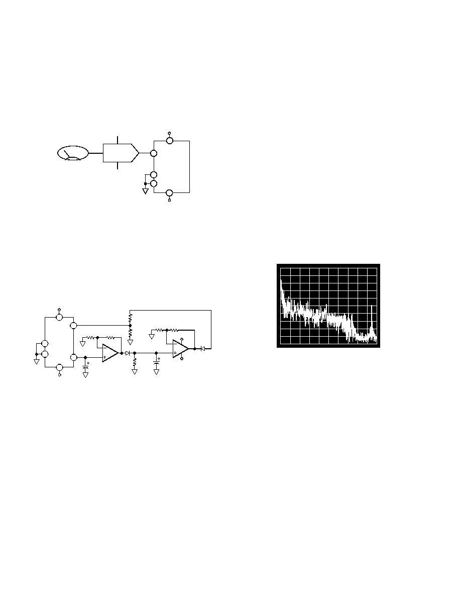
Prefiltering Out-of-Audio Band Tones
The most common cause of SSM2000 operational error is due
to large amplitude fixed-frequency tones. When SSM2000
detector's are exposed to large fixed-frequency tones, they rec-
ognizes these types of tones as signal and automatically adjust
the VCA and VCF to allow this frequency to pass through to the
output along with the underlying noise. The following is a list
of typical fixed-frequency tones which might cause this type
of HUSH behavior: switching power supply noise (20 kHz
200 kHz), sampling frequency in digitized music (44 kHz), PC
monitor scan frequency (30 kHz), microprocessor operating fre-
quency or submultiple, and FM stereo subcarrier frequency
(19 kHz). Figure 33 is a scope photo of a spectrum analyzer
output showing the 19 kHz FM stereo subcarrier frequency.
So, if your application will encounter any of these types of noise
sources, then a preconditioning filter for the internal detector is
necessary.
20Hz
20kHz
10dB/DIV
Figure 33. Scope Photo of the 19 kHz FM Subcarrier
Frequency
Figures 34 and 35 illustrate two different approaches to filtering
these undesired tones. If the interfering tone frequency is less
than 20 kHz (e.g., TV-15.625 kHz), a Twin-T Hi-Q notch filter
as shown in Figure 34 should be used. The notch filter will at-
tenuate the tone while having a minimal effect on the audio
band signal. For interfering tones above 20 kHz, a general
3-pole low-pass filter is recommended, such as the Butterworth
filter shown in Figure 35. The input of the filter should always
be connected to the output, SUM OUT. Filtering the SUM
OUT signal will not affect audio quality because the SUM
OUT signal is not part of the main audio path. However,
overaggressive filtering may remove noise and signal that is
necessary to set the VCA control, VCF control, and noise
threshold levels. The OP292 or OP275 shown in the example
filter circuit are high performance, low cost amplifiers suitable
for this application.
SSM2000
REV. 0
15
R
2
1k
2.2µF
SSM2000
8
R
1/2
OP275
R
R = 100k
C = 100pF
10k
2
3
1
C
2C
C
9
1k
VCF
DETECTOR
INPUT
SUM OUT
VCA
DETECTOR
INPUT
10
2.2nF
22nF
510
fc =
1
2
RC
22nF
Figure 34. A Hi-Q Twin-T Notch Filter with the Center
Frequency at 15.625 kHz
2.2µF
SSM2000
8
1k
1/2
OP275
1k
2
3
1
C
0.033µF
0.022µF
9
1k
VCF
DETECTOR
INPUT
SUM OUT
VCA
DETECTOR
INPUT
10
2.2nF
22nF
510
0.056µF
1k
22nF
Figure 35. A Three-Pole Butterworth Filter
Channel-to-Channel Separation
The SSM2000 has a 60 dB of channel separation specification
at 1 kHz. As shown in Figure 36, the Left input to the R VCF
node and the Right input to the L VCF node are tied together
with 50 k
of resistance, and tied to ground with 2.5 k
. If the
Left and Right ac coupling capacitors were not present this
would results in a dc separation of around 27 dB. However,
the inputs of the SSM2000 are usually ac coupled; therefore the
low frequency channel separation is a function of the value of
the ac coupling capacitors and the theoretical dc separation.
The higher the value of the ac coupling capacitor, the better the
channel separation will be. For example, using 10
µ
F ac cou-
pling capacitors will result in 32 dB of channel separation at
around 6 Hz8 Hz, improving at a rate of 20 dB/decade, till it
reaches a maximum 60 dB. Therefore, to achieve 60 dB of
channel separation at 75 Hz and above, 47
µ
F capacitors are
recommended.
6.8µF
L
R
2.5k
470pF
TO L VCF
10k
6.8µF
20k
20k
TO R VCF
TO DETECTORS
10k
2.5k
Figure 36. The SSM2000's Input Impedance Network
EVALUATING THE SSM2000
Because the SSM2000 is a dynamic system, it will respond to
test signals that are applied during the evaluation procedures.
Without thorough understanding of how the HUSH noise
reduction system works, attempts to apply standard test proce-
dures can produce misleading results. The following paragraphs
will present evaluation techniques to avoid many of these com-
mon evaluation pitfalls.
The SSM2000 has been designed as a stereo system. As a result
the input to the detector circuits is the sum of both the left and
right inputs. Monaural signals that used during evaluation
should be applied to both inputs, because the detectors' input
requires both the left and right signal. Otherwise, the control
levels from the VCA detector, VCF detector, and the Adaptive
Noise Threshold will be about one-half the necessary amplitude
for proper evaluation results.
The SSM2000 has exceptional tolerance for varying line levels
with noise reducing capability between line levels of 100 mV
rms to 1 V rms. However, the IC has been optimized for an in-
dustry standard input line level of 300 mV rms. Audio line lev-
els not equal to 300 mV rms will exhibit slightly degraded
specifications (e.g., distortion). If the line levels are outside of
the 100 mV rms to 1 V rms range, then audio output may appear
to have no noise reduction or to be muted. The circuit shown
in Figure 32 will enable noise reduction for very low line level
audio.
THD measurement instruments typically sweep a sine wave
across the audio spectrum. The normal SSM2000 response to
this type of signal results in the automatic noise threshold detec-
tor slowly rising to its maximum value; the VCA detector at
maximum value, the VCF detector will initially be closed at low
frequencies and will gradually open as the frequency is in-
creased. When the testing signal reaches about 500 Hz, it will
begin to be attenuated by the "closed" VCF. This attenuation
will reach at maximum of about 1 dB at 660 Hz for recom-
mended line levels, at which point the VCF detector begins to
open up. However, all these conditions and characteristics are
not representative of a normal music signal. To properly mea-
sure THD, it is necessary to activate HUSH Defeat. THD
measurements in DEFEAT mode give accurate results because
it does not remove the VCA and VCF from the signal chain,
rather it sets there values to unity (VCA) and maximum fre-
quency (VCF).
The bandwidth of the SSM2000, as stated before, is limited to
35 kHz because of the VCF capacitors. This bandwidth limita-
tion must be taken into account when the slew rate of the
SSM2000 is measured. The simplest method to measure slew
rate is to remove the VCF capacitors from the circuit, and take
the slew rate measurement while in DEFEAT mode. If the
VCF capacitors are not removed, then the audio signal is limited
by the VCF's bandwidth and not by the overall slew rate.
One standard of the SSM2000's audio quality is the characteris-
tics of the attack and release times of the VCA and VCF. The
attack and release times of the VCA and VCF are controlled by
1.1
µ
A current sources which charge the VCA Time Constant
capacitor and VCF Time Constant capacitor. The attack and
released times are typically measured from the VCA's and
VCF's fully closed position (e.g., VCA--maximum attenuation,
SSM2000
REV. 0
16
VCF--minimum bandwidth) to their fully open positions. If
the VCA and VCF are fully opened then at least 1.5 seconds of
no signal is required for the VCA and VCF detectors to return
to the closed position. A series of 10 kHz pulses interspersed
with 1.5 seconds of no signal will accomplish this requirement.
The system's attack and release times will be dominated by
VCA since the attack and release times of the VCA are slower
than the VCF's. In addition, monitoring Pins 11 (VCF) and 12
(VCA) will ensure that the VCA and VCF are either fully
opened or fully closed.
As stated before, the most common cause of a failure to reduce
noise is fixed-frequency tones that are being detected by the
output. A solution for this condition is detailed in the "Precau-
tions, Limitations, and Observations" section.
In single-supply applications, ACOM should be driven with a
well regulated reference capable of both sinking and souring
current. Zener-resistor references are unacceptable, because of
their inability to sink significant amounts of current.
By following these simple suggestions, the common pitfalls to a
successful implementation of the HUSH noise reduction system
can be avoided.
C2130105/96
PRINTED IN U.S.A.
OUTLINE DIMENSIONS
Dimensions shown in inches and (mm).
24-Pin Plastic DIP
(N-24)
24
1
12
13
0.280 (7.11)
0.240 (6.10)
PIN 1
1.275 (32.30)
1.125 (28.60)
0.150
(3.81)
MIN
0.200 (5.05)
0.125 (3.18)
SEATING
PLANE
0.022 (0.558)
0.014 (0.356)
0.060 (1.52)
0.015 (0.38)
0.210
(5.33)
MAX
0.070 (1.77)
0.045 (1.15)
0.100 (2.54)
BSC
0.325 (8.25)
0.300 (7.62)
0.015 (0.381)
0.008 (0.204)
0.195 (4.95)
0.115 (2.93)
24 Pin SOIC
(SOL-24)
24
13
12
1
0.6141 (15.60)
0.5985 (15.20)
0.4193 (10.65)
0.3937 (10.00)
0.2992 (7.60)
0.2914 (7.40)
PIN 1
SEATING
PLANE
0.0118 (0.30)
0.0040 (0.10)
0.0192 (0.49)
0.0138 (0.35)
0.1043 (2.65)
0.0926 (2.35)
0.0500
(1.27)
BSC
0.0125 (0.32)
0.0091 (0.23)
0.0500 (1.27)
0.0157 (0.40)
8
°
0
°
0.0291 (0.74)
0.0098 (0.25)
x 45
°
promotional and descriptive literature. Rocktron Corp. reserves the right to
approve use of the HUSH logo and may require submission of a schematic
illustrating the use of the SSM2000; a physical sample of the end product may
also be required. Applications for approval of the use of the HUSH name and
logo may be obtained by contacting ADI.
IMPORTANT NOTICE--LICENSING
The SSM2000 is manufactured under a license granted to Analog Devices,
Inc., by Rocktron Corp. and embodies technology covered by the following
patents: 4696044, 4893099, 5124657, 5263091, 5402498, and 5493617. For-
eign patents are pending. Rocktron Corp. grants a royalty-free license to
purchasers of the SSM2000 for use in end equipment, and no further rights
are implied. The use of the HUSH logo is encouraged on products, packaging,