 | ÐлекÑÑоннÑй компоненÑ: SSM2017P | СкаÑаÑÑ:  PDF PDF  ZIP ZIP |
Äîêóìåíòàöèÿ è îïèñàíèÿ www.docs.chipfind.ru
a
Self-Contained
Audio Preamplifier
SSM2017
One Technology Way, P.O. Box 9106, Norwood, MA 02062-9106, U.S.A.
Tel: 617/329-4700
World Wide Web Site: http://www.analog.com
Fax: 617/326-8703
© Analog Devices, Inc., 1997
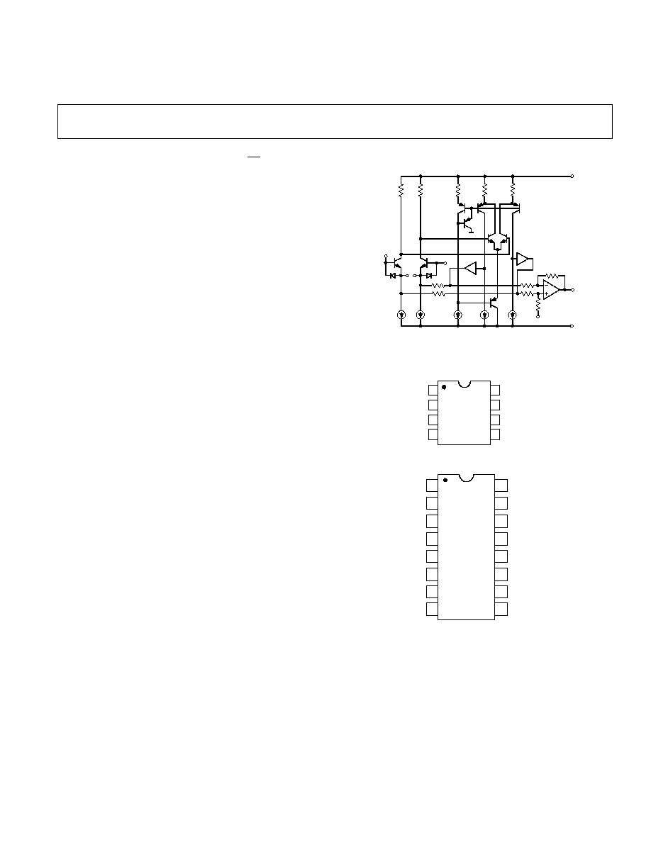
FUNCTIONAL BLOCK DIAGRAM
+IN
IN
OUT
5k
REFERENCE
RG
1
SSM2017
V+
X1
RG
2
V
X1
V
5k
5k
5k
5k
5k
PIN CONNECTIONS
Epoxy Mini-DIP (P Suffix)
REFERENCE
1
2
3
4
8
7
6
5
TOP VIEW
(Not to Scale)
IN
+IN
V
V+
OUT
RG
2
RG
1
SSM2017
16-Pin Wide Body SOL (S Suffix)
1
2
3
4
5
6
7
8
TOP VIEW
(Not to Scale)
16
15
14
13
12
11
10
9
NC
NC
IN
+IN
V
V+
OUT
REFERENCE
NC
NC
NC
NC
RG
1
RG
2
NC
NC
SSM2017
NC = NO CONNECT
TOP VIEW
(Not to Scale)
FEATURES
Excellent Noise Performance: 950 pV/
Hz or 1.5 dB
Noise Figure
Ultralow THD: < 0.01% @ G = 100 Over the Full Audio
Band
Wide Bandwidth: 1 MHz @ G = 100
High Slew Rate: 17 V/ s typ
Unity Gain Stable
True Differential Inputs
Subaudio 1/f Noise Corner
8-Pin Mini-DIP with Only One External Component
Required
Very Low Cost
Extended Temperature Range: 40 C to +85 C
APPLICATIONS
Audio Mix Consoles
Intercom/Paging Systems
Two-Way Radio
Sonar
Digital Audio Systems
REV. C
Information furnished by Analog Devices is believed to be accurate and
reliable. However, no responsibility is assumed by Analog Devices for its
use, nor for any infringements of patents or other rights of third parties
which may result from its use. No license is granted by implication or
otherwise under any patent or patent rights of Analog Devices.
GENERAL DESCRIPTION
The SSM2017 is a latest generation audio preamplifier, combin-
ing SSM preamplifier design expertise with advanced process-
ing. The result is excellent audio performance from a self-
contained 8-pin mini-DIP device, requiring only one external
gain set resistor or potentiometer. The SSM2017 is further en-
hanced by its unity gain stability.
Key specifications include ultralow noise (1.5 dB noise figure)
and THD (<0.01% at G = 100), complemented by wide band-
width and high slew rate.
Applications for this low cost device include microphone pream-
plifiers and bus summing amplifiers in professional and con-
sumer audio equipment, sonar, and other applications requiring
a low noise instrumentation amplifier with high gain capability.
SSM2017SPECIFICATIONS
(V
S
= 15 V and 40 C
T
A
+85 C, unless otherwise noted. Typical speci-
fications apply at T
A
= +25 C.)
Parameter
Symbol
Conditions
Min
Typ
Max
Units
DISTORTION PERFORMANCE
T
A
= +25
°
C
V
O
= 7 V rms
R
L
= 5 k
Total Harmonic Distortion Plus Noise
THD+N
G = 1000, f = 1 kHz
0.012
%
G = 100, f = 1 kHz
0.005
%
G = 10, f = 1 kHz
0.004
%
G = 1, f = 1 kHz
0.008
%
NOISE PERFORMANCE
Input Referred Voltage Noise Density
e
n
f = 1 kHz, G = 1000
0.95
nV/
Hz
f = 1 kHz; G = 100
1.95
nV/
Hz
f = 1 kHz; G = 10
11.83
nV/
Hz
f = 1 kHz; G = 1
107.14
nV/
Hz
Input Current Noise Density
i
n
f = 1 kHz, G = 1000
2
pA/
Hz
DYNAMIC RESPONSE
Slew Rate
SR
G = 10
10
17
V/
µ
s
R
L
= 4.7 k
C
L
= 50 pF
T
A
= +25
°
C
Small Signal Bandwidth
BW
3 dB
G = 1000
200
kHz
G = 100
1000
kHz
G = 10
2000
kHz
G = 1
4000
kHz
INPUT
Input Offset Voltage
V
IOS
0.1
1.2
mV
Input Bias Current
I
B
V
CM
= 0 V
6
25
µ
A
Input Offset Current
Ios
V
CM
= 0 V
±
0.002
±
2.5
µ
A
Common-Mode Rejection
CMR
V
CM
=
±
8 V
G = 1000
80
112
dB
G = 100
60
92
dB
G = 10
40
74
dB
G = 1, T
A
= +25
°
C
26
54
dB
G = 1, T
A
= 40
°
C to +85
°
C
20
54
dB
Power Supply Rejection
PSR
V
S
=
±
6 V to
±
18 V
G = 1000
80
124
dB
G = 100
60
118
dB
G = 10
40
101
dB
G = 1
26
82
dB
Input Voltage Range
IVR
±
8
V
Input Resistance
R
IN
Differential, G = 1000
1
M
G = 1
30
M
Common Mode, G = 1000
5.3
M
G = 1
7.1
M
OUTPUT
Output Voltage Swing
V
O
R
L
= 2 k
; T
A
= +25
°
C
±
11.0
±
12.3
V
Output Offset Voltage
V
OOS
40
500
mV
Minimum Resistive Load Drive
T
A
= +25
°
C
2
k
T
A
= 40
°
C to +85
°
C
4.7
k
Maximum Capacitive Load Drive
50
pF
Short Circuit Current Limit
I
SC
Output-to-Ground Short
±
50
mA
Output Short Circuit Duration
10
sec
GAIN
Gain Accuracy
R
G
=
10 k
T
A
= +25
°
C
G 1
R
G
= 10
, G = 1000
0.25
1
dB
R
G
= 101
, G = 100
0.20
1
dB
R
G
= 1.1 k
, G = 10
0.20
1
dB
R
G
= , G = 1
0.05
0.5
dB
Maximum Gain
G
70
dB
REFERENCE INPUT
Input Resistance
10
k
Voltage Range
±
8
V
Gain to Output
1
V/V
POWER SUPPLY
Supply Voltage Range
V
S
±
6
±
22
V
Supply Current
I
SY
V
CM
= 0 V, R
L
=
±
10.6
±
14.0
mA
Specifications subject to change without notice.
REV. C
2
SSM2017
3
REV. C
WARNING!
ESD SENSITIVE DEVICE
CAUTION
ESD (electrostatic discharge) sensitive device. Electrostatic charges as high as 4000 V readily
accumulate on the human body and test equipment and can discharge without detection.
Although the SSM2017 features proprietary ESD protection circuitry, permanent damage may
occur on devices subjected to high energy electrostatic discharges. Therefore, proper ESD
precautions are recommended to avoid performance degradation or loss of functionality.
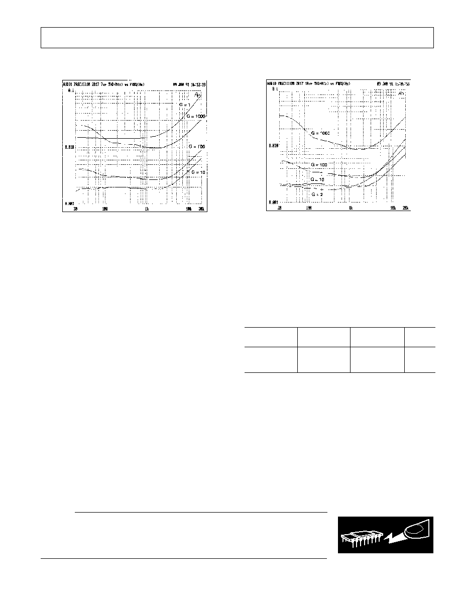
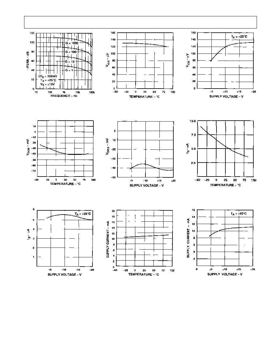
Typical Performance Characteristics
Figure 1. Typical THD+Noise* at G = 1, 10, 100, 1000;
V
O
= 7 V rms, V
S
=
±
15 V, R
L
= 5 k
; T
A
= +25
°
C
*80 kHz low-pass filter used for Figures 1-2.
ABSOLUTE MAXIMUM RATINGS
Supply Voltage . . . . . . . . . . . . . . . . . . . . . . . . . . . . . . . .
±
22 V
Input Voltage . . . . . . . . . . . . . . . . . . . . . . . . . . Supply Voltage
Output Short Circuit Duration . . . . . . . . . . . . . . . . . . . 10 sec
Storage Temperature Range (P, Z Packages) 65
°
C to +150
°
C
Junction Temperature (T
J
) . . . . . . . . . . . . . 65
°
C to +150
°
C
Lead Temperature Range (Soldering, 60 sec) . . . . . . . . 300
°
C
Operating Temperature Range . . . . . . . . . . . . 40
°
C to +85
°
C
Thermal Resistance*
8-Pin Hermetic DIP (Z):
JA
= 134;
JC
= 12 . . . . . .
°
C/W
8-Pin Plastic DIP (P):
JA
= 96;
JC
= 37 . . . . . . . . . .
°
C/W
16-Pin SOIC (S):
JA
= 92;
JC
= 27 . . . . . . . . . . . . .
°
C/W
*
JA
is specified for worst case mounting conditions, i.e.,
JA
is specified for device
in socket for cerdip and plastic DIP;
JA
is specified for device soldered to printed
circuit board for SOL package.
ORDERING GUIDE
Temperature
Package
Package
Model
Range*
Description
Option
SSM2017P
40
°
C to +85
°
C
8-Pin Plastic DIP
N-8
SSM2017S
40
°
C to +85
°
C
16-Lead SOL
R-16
SSM2017S-REEL
40
°
C to +85
°
C
16-Lead SOL
R-16
*XIND = 40
°
C to +85
°
C.
Figure 2. Typical THD+ Noise * at G = 2, 10, 100, 1000;
V
O
= 10 V rms, V
S
=
±
18 V, R
L
= 5 k
; T
A
= +25
°
C
SSM2017
4
REV. C
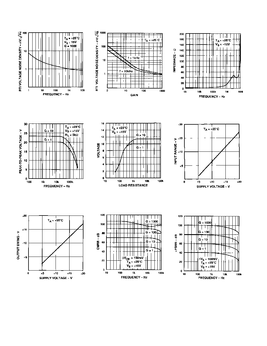
Figure 3. Voltage Noise Density vs.
Frequency
Figure 6. Maximum Output Swing
vs. Frequency
Figure 9. Output Voltage Range vs.
Supply Voltage
Figure 4. RTI Voltage Noise Density
vs. Gain
Figure 7. Maximum Output Voltage
vs. Load Resistance
Figure 10. CMRR vs. Frequency
Figure 5. Output Impedance vs.
Frequency
Figure 8. Input Voltage Range vs.
Supply Voltage
Figure 11. +PSRR vs. Frequency
SSM2017
5
REV. C
Figure 12. PSRR vs. Frequency
Figure 15. V
OOS
vs. Temperature
Figure 18. I
B
vs. Supply Voltage
Figure 13. V
IOS
vs. Temperature
Figure 16. V
OOS
vs. Supply Voltage
Figure 19. I
SY
vs. Temperature
Figure 14. V
IOS
vs. Supply Voltage
Figure 17. I
B
vs. Temperature
Figure 20. I
SY
vs. Supply Voltage
SSM2017
6
REV. C
Figure 21. Bandwidth of the SSM2017 for Various Values
of Gain
NOISE PERFORMANCE
The SSM2017 is a very low noise audio preamplifier exhibiting
a typical voltage noise density of only 1 nV/
Hz at 1 kHz. The
exceptionally low noise characteristics of the SSM2017 are in
part achieved by operating the input transistors at high collector
currents since the voltage noise is inversely proportional to the
square root of the collector current. Current noise, however, is
directly proportional to the square root of the collector current.
As a result, the outstanding voltage noise performance of the
SSM2017 is obtained at the expense of current noise perfor-
mance. At low preamplifier gains, the effect of the SSM2017's
voltage and current noise is insignificant.
The total noise of an audio preamplifier channel can be calcu-
late by:
E
n
=
e
n
2
+
(i
n
R
S
)
2
+
e
t
2
where:
E
n
= total input referred noise
e
n
= amplifier voltage noise
i
n
= amplifier current noise
R
S
= source resistance
e
t
= source resistance thermal noise.
For a microphone preamplifier, using a typical microphone im-
pedance of 150
the total input referred noise is:
e
n
= 1 nV/
Hz @ 1 kHz, SSM2017 e
n
i
n
= 2 pA/
Hz @ 1 kHz, SSM2017 i
n
R
S
= 150
, microphone source impedance
e
t
= 1.6 nV/
Hz @ 1 kHz, microphone thermal noise
E
n
=
(1 nV
Hz)
2
+ 2 (pA/
Hz
×
150
)
2
+ (1.6 nV/
Hz)
2
= 1.93 nV/
Hz @ 1 kHz.
This total noise is extremely low and makes the SSM2017
virtually transparent to the user.
A
V
dB
R
G
1
0
NC
3.2
10
4.7k
10
20
1.1k
31.3
30
330
100
40
100
314
50
32
1000
60
10
G =
V
OUT
(+In) (In)
=
10 k
R
G
+1
Basic Circuit Connections
GAIN
The SSM2017 only requires a single external resistor to set the
voltage gain. The voltage gain, G, is:
G =
10 k
R
G
+1
and
R
G
=
10 k
G 1
For convenience, Table I lists various values of R
G
for common
gain levels.
Table I. Values of R
G
for Various Gain Levels
The voltage gain can range from 1 to 3500. A gain set resistor is
not required for unity gain applications. Metal-film or wire-
wound resistors are recommended for best results.
The total gain accuracy of the SSM2017 is determined by the
tolerance of the external gain set resistor, R
G
, combined with the
gain equation accuracy of the SSM2017. Total gain drift com-
bines the mismatch of the external gain set resistor drift with
that of the internal resistors (20 ppm/
°
C typ).
Bandwidth of the SSM2017 is relatively independent of gain as
shown in Figure 21. For a voltage gain of 1000, the SSM2017
has a small-signal bandwidth of 200 kHz. At unity gain, the
bandwidth of the SSM2017 exceeds 4 MHz.
SSM2017
7
REV. C
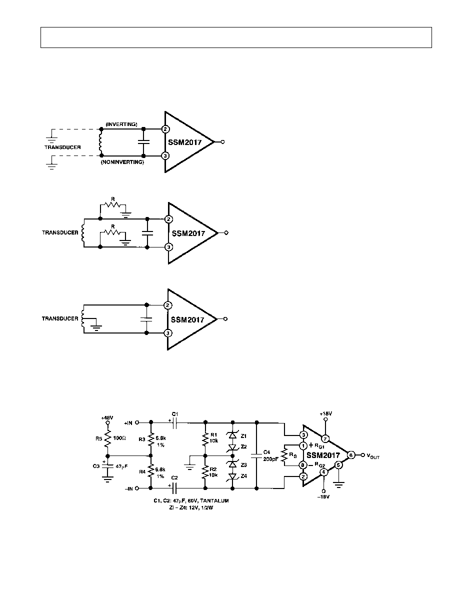
Figure 23. SSM2017 in Phantom Powered Microphone Circuit
INPUTS
The SSM2017 has protection diodes across the base emitter
junctions of the input transistors. These prevent accidental ava-
lanche breakdown, which could seriously degrade noise perfor-
mance. Additional clamp diodes are also provided to prevent the
inputs from being forced too far beyond the supplies.
a. Single Ended
b. Pseudo Differential
c. True Differential
Figure 22. Three Ways of Interfacing Transducers for High
Noise Immunity
Although the SSM2017's inputs are fully floating, care must be
exercised to ensure that both inputs have a dc bias connection
capable of maintaining them within the input common-mode
range. The usual method of achieving this is to ground one side
of the transducer as in Figure 22a, but an alternative way is to
float the transducer and use two resistors to set the bias point as
in Figure 22b. The value of these resistors can be up to 10 k
,
but they should be kept as small as possible to limit common-
mode pickup. Noise contribution by resistors themselves is neg-
ligible since it is attenuated by the transducer's impedance. Bal-
anced transducers give the best noise immunity and interface
directly as in Figure 22c.
REFERENCE TERMINAL
The output signal is specified with respect to the reference ter-
minal, which is normally connected to analog ground. The ref-
erence may also be used for offset correction or level shifting. A
reference source resistance will reduce the common-mode rejec-
tion by the ratio of 5 k
/R
REF
. If the reference source resis-
tance is 1
, then the CMR will be reduced to 74 dB (5 k
/1
= 74 dB).
COMMON-MODE REJECTION
Ideally, a microphone preamplifier responds only to the differ-
ence between the two input signals and rejects common-mode
voltages and noise. In practice, there is a small change in output
voltage when both inputs experience the same common-mode
voltage change; the ratio of these voltages is called the common-
mode gain. Common-mode rejection (CMR) is the logarithm of
the ratio of differential-mode gain to common-mode gain,
expressed in dB.
PHANTOM POWERING
A typical phantom microphone powering circuit is shown in
Figure 23. Z
1
through Z
4
provide transient overvoltage protec-
tion for the SSM2017 whenever microphones are plugged in or
unplugged.
SSM2017
8
REV. C
C1534244/91
PRINTED IN U.S.A.
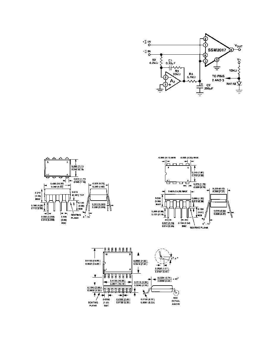
BUS SUMMING AMPLIFIER
In addition to is use as a microphone preamplifier, the SSM2017
can be used as a very low noise summing amplifier. Such a cir-
cuit is particularly useful when many medium impedance out-
puts are summed together to produce a high effective noise gain.
The principle of the summing amplifier is to ground the SSM2017
inputs. Under these conditions, Pins 1 and 8 are ac virtual
grounds sitting about 0.55 V below ground.
To remove the 0.55 V offset, the circuit of Figure 24 is
recommended.
A
2
forms a "servo" amplifier feeding the SSM2017's inputs.
This places Pins l and 8 at a true dc virtual ground. R4 in con-
junction with C2 remove the voltage noise of A
2
, and in fact just
about any operational amplifier will work well here since it is re-
moved from the signal path. If the dc offset at Pins l and 8 is not
too critical, then the servo loop can be replaced by the diode bi-
asing scheme of Figure 24. If ac coupling is used throughout,
then Pins 2 and 3 may be directly grounded.
Figure 24. Bus Summing Amplifier
OUTLINE DIMENSIONS
Dimensions shown in inches and (mm).
8-Pin Plastic DIP (P) Package
8-Pin Hermetic DIP (Z) Package
16-Pin SOIC (S) Package