 | ÐлекÑÑоннÑй компоненÑ: SSM2122 | СкаÑаÑÑ:  PDF PDF  ZIP ZIP |
Äîêóìåíòàöèÿ è îïèñàíèÿ www.docs.chipfind.ru
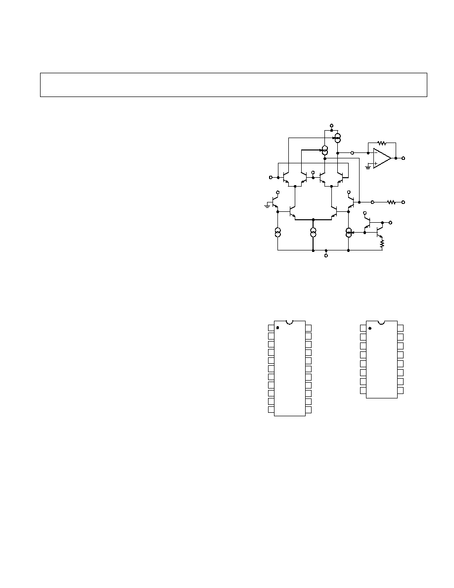
FUNCTIONAL BLOCK DIAGRAM
SIGNAL
OUT
CURRENT
MIRRORS
V
C
+V
C
V+
V+
V+
SIGNAL
INPUT
36k
36k
V+
V
I
REF
REV. C
Information furnished by Analog Devices is believed to be accurate and
reliable. However, no responsibility is assumed by Analog Devices for its
use, nor for any infringements of patents or other rights of third parties
which may result from its use. No license is granted by implication or
otherwise under any patent or patent rights of Analog Devices.
a
Dynamic Range
Processors/Dual VCA
SSM2120/SSM2122
© Analog Devices, Inc., 1995
One Technology Way, P.O. Box 9106, Norwood, MA 02062-9106, U.S.A.
Tel: 617/329-4700
Fax: 617/326-8703
GENERAL DESCRIPTION
The SSM2120 is a monolithic integrated circuit designed for the
purpose of processing dynamic signals in various analog systems
including audio. This "dynamic range processor" consists of two
VCAs and two level detectors (the SSM2122 consists of two
VCAs only). These circuit blocks allow the user to logarithmically
control the gain or attenuation of the signals presented to the
level detectors depending on their magnitudes. This allows the
compression, expansion or limiting of ac signals, some of the
primary applications for the SSM2120.
FEATURES
0.01% THD at +10 dBV In/Out
100 dB VCA Dynamic Range
Low VCA Control Feedthrough
100 dB Level Detection Range
Log/Antilog Control Paths
Low External Component Count
APPLICATIONS
Compressors
Expanders
Limiters
AGC Circuits
Voltage-Controlled Filters
Noise Reduction Systems
Stereo Noise Gates
PIN CONNECTIONS
22-Pin Plastic DIP
(P Suffix)
16-Pin Plastic DIP
(P Suffix)
13
16
15
14
22
21
20
19
18
17
12
TOP VIEW
(Not to Scale)
11
10
9
8
1
2
3
4
7
6
5
SSM2120
THRESH 1
+V
C2
SIG
OUT 2
V+
GND
LOG AV 1
CON
OUT 1
SIG
OUT 1
SIG
IN 2
V
C2
CFT 2
+V
C1
CFT 1
V
C1
SIG
IN 1
REC
IN 1
I
REF
LOG AV 2
CON
OUT 2
REC
IN 2
V
THRESH 2
14
13
12
11
16
15
10
9
8
1
2
3
4
7
6
5
TOP VIEW
(Not to Scale)
SSM2122
GND
+V
C2
SIG
OUT 2
V+
GND
SIG
OUT 1
+V
C1
CFT 1
SIG
IN 2
V
C2
CFT 2
V
C1
SIG
IN 1
I
REF
V
GND

SSM2120/SSM2122SPECIFICATIONS
ELECTRICAL CHARACTERISTICS
REV. C
2
SSM2120/SSM2122
Parameter
Conditions
Min
Typ
Max
Units
POWER SUPPLY
Supply Voltage Range
±
5
±
18
V
Positive Supply Current
8
10
mA
Negative Supply Current
6
8
mA
VCAs
Max I
SIGNAL
(In/Out)
±
300
±
325
±
350
µ
A
Output Offset
±
1
±
8
µ
A
Control Feedthrough (Trimmed)
R
IN
= R
OUT
= 36 k
, 30 dB
A
V
0 dB
±
750
µ
V
Gain Control Range
Unity-Gain
85
+40
dB
Control Sensitivity
6
mV/dB
Gain Scale Factor Drift
3300
ppm/
°
C
Frequency Response
Unity Gain or Less
250
kHz
Off Isolation
At 1 kHz
100
dB
Current Gain
+V
C
= V
C
= 0 V
0.5
+0.5
dB
THD (Unity-Gain)
+10 dBV IN/OUT
0.005
0.04
%
Noise (20 kHz Bandwidth)
RE: 0 dBV
80
dB
LEVEL DETECTORS (SSM2120 ONLY)
Detection Range
90
95
dB
Input Current Range
0.085
2800
µ
A p-p
Rectifier Input Bias Current
4
nA
Output Sensitivity (At LOG AV Pin)
3
mV/dB
Output Offset Voltage
±
0.5
±
3.4
mV
Frequency Response
I
IN
= 1 mA p-p
1000
I
IN
= 10
µ
A p-p
50
kHz
I
IN
= 1
µ
A p-p
7.5
CONTROL AMPLIFIERS (SSM2120 ONLY)
Input Bias Current
±
85
±
175
nA
Output Drive (Max Sink Current)
5.0
7.5
mA
Input Offset Voltage
±
0.5
±
4.2
mV
Specifications are subject to change without notice.
(@V
S
= 15 V, T
A
= +25 C, I
REF
= 200 A, +V
C
= V
C
= GND (A
V
= 0 dB). 0 dB = 1 V rms
unless otherwise noted)
ABSOLUTE MAXIMUM RATINGS
Supply Voltage . . . . . . . . . . . . . . . . . . . . . . . . . . . . . . . .
±
18 V
Operating Temperature Range . . . . . . . . . . . . 10
°
C to +55
°
C
Junction Temperature . . . . . . . . . . . . . . . . . . . . . . . . . +150
°
C
Storage Temperature . . . . . . . . . . . . . . . . . . 65
°
C to +150
°
C
Maximum Current into Any Pin . . . . . . . . . . . . . . . . . . 10 mA
Lead Temperature Range (Soldering, 60 sec) . . . . . . . +300
°
C
Package Type
JA
1
JC
Units
16-Pin Plastic DIP (P)
86
10
°
C/W
22-Pin Plastic DIP (P)
70
7
°
C/W
NOTE
1
JA
is specified for worst case mounting conditions, i.e.,
JA
is specified for
device in socket for P-DIP.
ORDERING GUIDE
Temperature
Package
Package
Model
Range
Description
Option
SSM2120
10
°
C to +50
°
C
22-Pin Plastic DIP
(N-22)
SSM2122
10
°
C to +50
°
C
16-Pin Plastic DIP
(N-16)
WARNING!
ESD SENSITIVE DEVICE
CAUTION
ESD (electrostatic discharge) sensitive device. Electrostatic charges as high as 4000 V readily
accumulate on the human body and test equipment and can discharge without detection.
Although the SSM2120/SSM2122 features proprietary ESD protection circuitry, permanent damage
may occur on devices subjected to high energy electrostatic discharges. Therefore, proper ESD
precautions are recommended to avoid performance degradation or loss of functionality.
SSM2120/SSM2122
REV. C
3
2V
FULL
WAVE
RECTIFIER
|I
I N
|
V+
THRESH 2
LOG AV 2
V
CON
OUT 2
REC
IN 2
+V
C1
CFT 1
V
C1
INPUT 1
OUTPUT 1
+V
C2
CFT 2
V
C2
INPUT 2
OUTPUT 2
SSM2122
2V
FULL
WAVE
RECTIFIER
|I
I N
|
V+
THRESH 1
LOG AV 1
V
CON
OUT 1
REC
IN 1
Figure 1. SSM2120 Block Diagram
VCA PERFORMANCE
Figures 2a and 2b show the typical THD and noise performance
of the VCAs over
±
20 dB gain/attenuation. Full Class A operation
provides very low THD.
GAIN dB
0.03
THD %
0.01
20
20
10
0
10
0.003
a. VCA THD Performance vs. Gain
(+10 dBV In/Out @ 1 kHz)
GAIN dB
70
80
20
20
10
0
10
90
NOISE dBV
b. VCA Noise vs. Gain (20 kHz Bandwidth)
Figure 2. Typical THD and Noise Performance
VOLTAGE-CONTROLLED AMPLIFIERS
The two voltage-controlled amplifiers are full Class A current
in/current out devices with complementary dB/V gain control
ports. The control sensitivities are +6 mV/dB and 6 mV/dB. A
resistor divider (attenuator) is used to adapt the sensitivity of an
external control voltage to the range of the control port. It is
best to use 200
or less for the attenuator resistor to ground.
VCA INPUTS
The signal inputs behave as virtual grounds. The input current
compliance range is determined by the current into the reference
current pin.
REFERENCE PIN
The reference current determines the input and output current
compliance range of the VCAs. The current into the reference
pin is set by connecting a resistor to V+. The voltage at the
reference pin is about two volts above V and the current will be
I
REF
=
[(V
+
) ((V )
+
2 V )]
R
REF
The current consumption of the VCAs will be directly pro-
portional to I
REF
which is nominally 200
µ
A. The device will
operate at lower current levels which will reduce the effective
dynamic range of the VCAs. With a 200
µ
A reference current,
the input and output clip points will be
±
400
µ
A. In general:
I
CLIP
=
±
2 I
REF
VCA OUTPUTS
The VCA outputs are designed to interface directly with the virtual
ground inputs of external operational amplifiers configured as
current-to-voltage converters. The outputs must operate at virtual
ground because of the output stage's finite output impedance.
The power supplies and selected compliance range determines
the values of input and output resistors needed. As an example,
with
±
15 V supplies and
±
400
µ
A maximum input and output
current, choose R
IN
= R
OUT
= 36 k
for an output compliance
range of
±
14.4 V. Note that the signal path through the VCA
including the output current-to-voltage converter is noninverting.
SSM2120/SSM2122
REV. C
4
2V
FULL
WAVE
RECTIFIER
|I
I N
|
V+
THRESH
LOG AV
V
CON
OUT
REC
IN
Q1
Q2
I
REF
1k
39k
200
R
CON
TO V
C
R
IN
INPUT
V
R
REF
C
AV
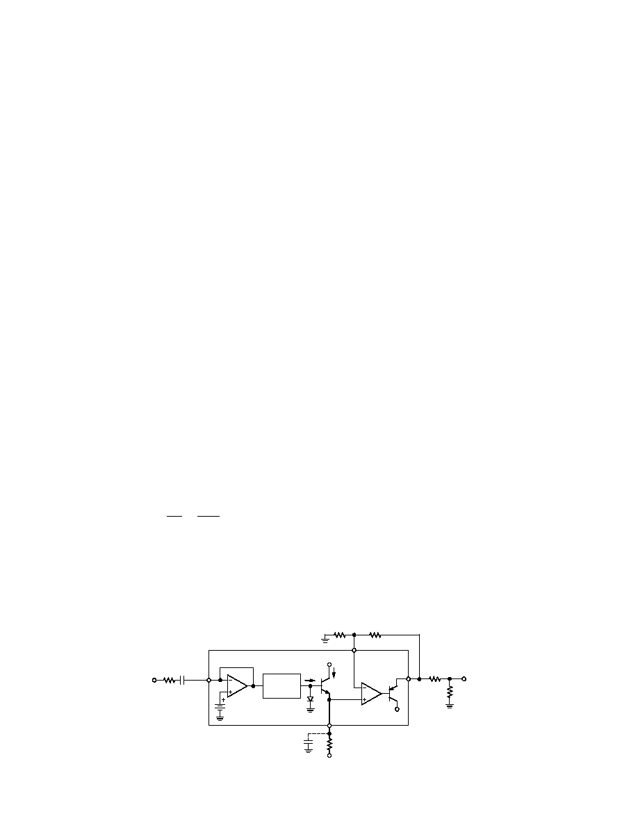
Figure 3. Level Detector
Note: It is natural to assume that with the addition of the
averaging capacitor, the LOG AV output would become the
average of the log of the absolute value of I
IN
. However, since the
capacitor forces an ac ground at the emitter of the output
transistor, the capacitor charging currents are proportional to
the antilog of the voltage at the base of the output transistor.
Since the base voltage of the output transistor is the log of the
absolute value of I
IN
, the log and antilog terms cancel, so the
capacitor becomes a linear integrator with a charging current
directly proportional to the absolute value of the input current.
This effectively inverts the order of the averaging and logging
functions. The signal at the output therefore is the log of the
average of the absolute value of I
IN
.
USING DETECTOR PINS REC
IN
, LOG
AV
, THRESH AND
CON
OUT
When applying signals to REC
IN
(rectifier input) an input series
resistor should be followed by a low leakage blocking capacitor
since REC
IN
has a dc voltage of approximately 2.1 V above
ground. Choose R
IN
for a
±
1.5 mA peak signal. For
±
15 V
operation this corresponds to a value of 10 k
.
A 1.5 M
value of R
REF
from log average to 15 V will establish
a 10
µ
A reference current in the logging transistor (Q
1
). This
will bias the transistor in the middle of the detector's dynamic
current range in dB to optimize dynamic range and accuracy.
The LOG AV outputs are buffered and amplified by unipolar
drive op amps. The 39 k
, 1 k
resistor network at the
THRESH pin provides a gain of 40.
An attenuator from the CON
OUT
(control output) to the
appropriate VCA control port establishes the control sensitivity.
Use 200
for the attenuator resistor to ground and choose
R
CON
for the desired sensitivity. Care should be taken to minimize
capacitive loads on the control outputs CON
OUT
. If long lines
or capacitive loads are present, it is best to connect the series
resistor R
CON
as closely to the CON
OUT
pin as possible.
DYNAMIC LEVEL DETECTOR CHARACTERISTICS
Figures 4 and 5 show the dynamic performance of the level
detector to a change in signal level. The input to the detector (not
shown) is a series of 500 ms tone bursts at 1 kHz in successive
10 dBV steps. The tone bursts start at a level of 60 dBV (with
R
IN
= 10 k) and return to 60 dBV after each successive 10 dB
step. Tone bursts range from 60 dBV to +10 dBV. Figure 4
shows the logarithmic level detector output. The output of the
detector is 3 mV/dB at LOG AV and the amplifier gain is 40
which yields 120 mV/dB. Thus, the output at CON
OUT
is seen
to increase by 1.2 V for each 10 dBV increase in input level.
TRIMMING THE VCAs
The control feedthrough (CFT) pins are optional control feed-
through null points. CFT nulling is usually required in applications
such as noise gating and downward expansion. If trimming is
not used, leave the CFT pins open.
Trim Procedure
1. Apply a 100 Hz sine wave to the control point attenuator.
The signal peaks should correspond to the control voltages
which induce the VCAs maximum intended gain and at least
30 dB of attenuation.
2. Adjust the 50 k
potentiometer for the minimum
feedthrough.
(Trimmed control feedthrough is typically well under 1 mV rms
when the maximum gain is unity using 36 k
input and output
resistors.)
Applications such as compressor/limiters typically do not require
control feedthrough trimming because the VCA operates at
unity-gain unless the signal is large enough to initiate gain
reduction. In this case the signal masks control feedthrough.
This trim is ineffective for voltage-controlled filter applications.
LEVEL DETECTION CIRCUITS
The SSM2120 contains two independent level detection
circuits. Each circuit contains a wide dynamic range full-wave
rectifier, logging circuit and a unipolar drive amplifier. These
circuits will accurately detect the input signal level over a
100 dB range from 30 nA to 3 mA peak-to-peak.
LEVEL DETECTOR THEORY OF OPERATION
Referring to the level detector block diagram of Figure 3, the
REC
IN
input is an AC virtual ground. The next block imple-
ments the full-wave rectification of the input current. This
current is then fed into a logging transistor (Q
1
) whose pair
transistor (Q
2
) has a fixed collector current of I
REF
. The LOG
AV output is then:
V
LOG
AV
=
kT
q
ln
|I
IN
|
I
REF
With the use of the LOG AV capacitor the output is then the log
of the average of the absolute value of I
IN
.
(The unfiltered LOG AV output has broad flat plateaus with
sharp negative spikes at the zero crossing. This reduces the
"work" that the averaging capacitor must do, particularly at low
frequencies.)
SSM2120/SSM2122
REV. C
5
The decay rates are linear ramps that are dependent on the
current out of the LOG AV pin (set by R
REF
) and the value of
C
AV
. The integration or decay time of the circuit is derived from
the formula:
Decrementation Rate (in dB/s) =
I
REF
×
333
C
AV
Table I. Settling Time (t
S
) for C
AV
= 10 F. t
S
= t
S
(C
AV
= 10 F)
5 dB
3 dB
2 dB
1 dB
10 dB Step
11.28 ms
21.46
30.19
46.09
20 dB Step
16.65
26.83
35.56
51.46
30 dB Step
18.15
28.33
37.06
52.96
40 dB Step
18.61
27.79
37.52
53.42
50 dB Step
(+144
µ
s)
60 dB Step
(+46
µ
s)
APPLICATIONS
The following applications for the SSM2120 use both the VCAs
and level detectors in conjunction to assimilate a variety of
functions.
The first section describes the arrangement of the threshold
control in each control circuit configuration. These control
circuits form the foundation for the applications to follow which
include the downward expander, compressor/limiter and
compandor.
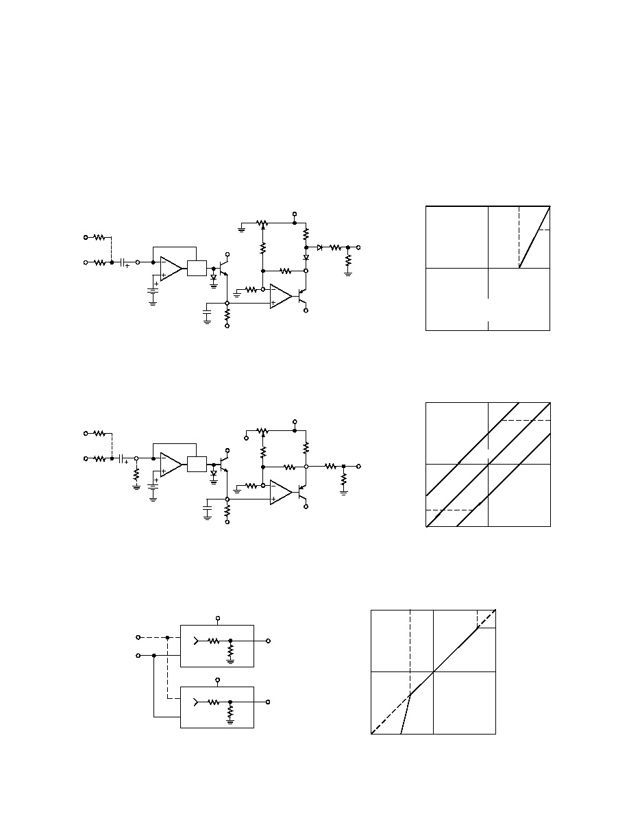
THRESHOLD CONTROL
Figure 6a shows the control circuit for a typical downward
expander while Figure 6b shows a typical control curve. Here,
the threshold potentiometer adjusts V
T
to provide a negative
unipolar control output. This is typically used in noise gate,
downward expander, and dynamic filter applications. This
potentiometer is used in all applications to control the signal
level versus control voltage characteristics.
10
0%
100
90
1s
2V
Figure 4. Detector Output
10
0%
100
90
2V
50ms
Figure 5. Overlayed Detector Output
DYNAMIC ATTACK AND DECAY RATES
Figure 5 shows the output levels overlayed using a storage
scope. The attack rate is determined by the step size and the
value of C
AV
. The attack time to final value is a function of the
step size increase. Table I shows the values of total settling
times to within 5 dB, 3 dB, 2 dB and 1 dB of final value with
C
AV
= 10
µ
F. When step sizes exceed 40 dB, the increase in
settling time for larger steps is negligible. To calculate the attack
time to final value for any value of C
AV
, simply multiply the
value in the chart by C
AV
/10
µ
F.
V
IN
dB
+
*LOWER LIMIT CAN BE FIXED
BY CONNECTING A RESISTOR
R
LL
FROM REC
IN
TO GROUND
THRESHOLD
V
CON
*
2V
|I
I N
|
V+
V
CON
OUT
REC
IN
39k
200
R
CON
TO +V
C
R
IN
MONO
OR R
C
AV
R
LL
R
T
THRESHOLD
CONTROL
LOG AV
R
IN
L
MONO R
IN
= 10k
STEREO R
IN
= 20k
V
1.5M
1k
V
V
T
a. Control Circuit b. Typical Downward Expander
Control Curve
Figure 6. Noise Gate/Downward Expander Control Circuit and Typical Response
SSM2120/SSM2122
REV. C
6
In the noise gate, downward expander and compressor/limiter
applications, this potentiometer will establish the onset of the
control action. The sensitivity of the control action depends on
the value of R
T
.
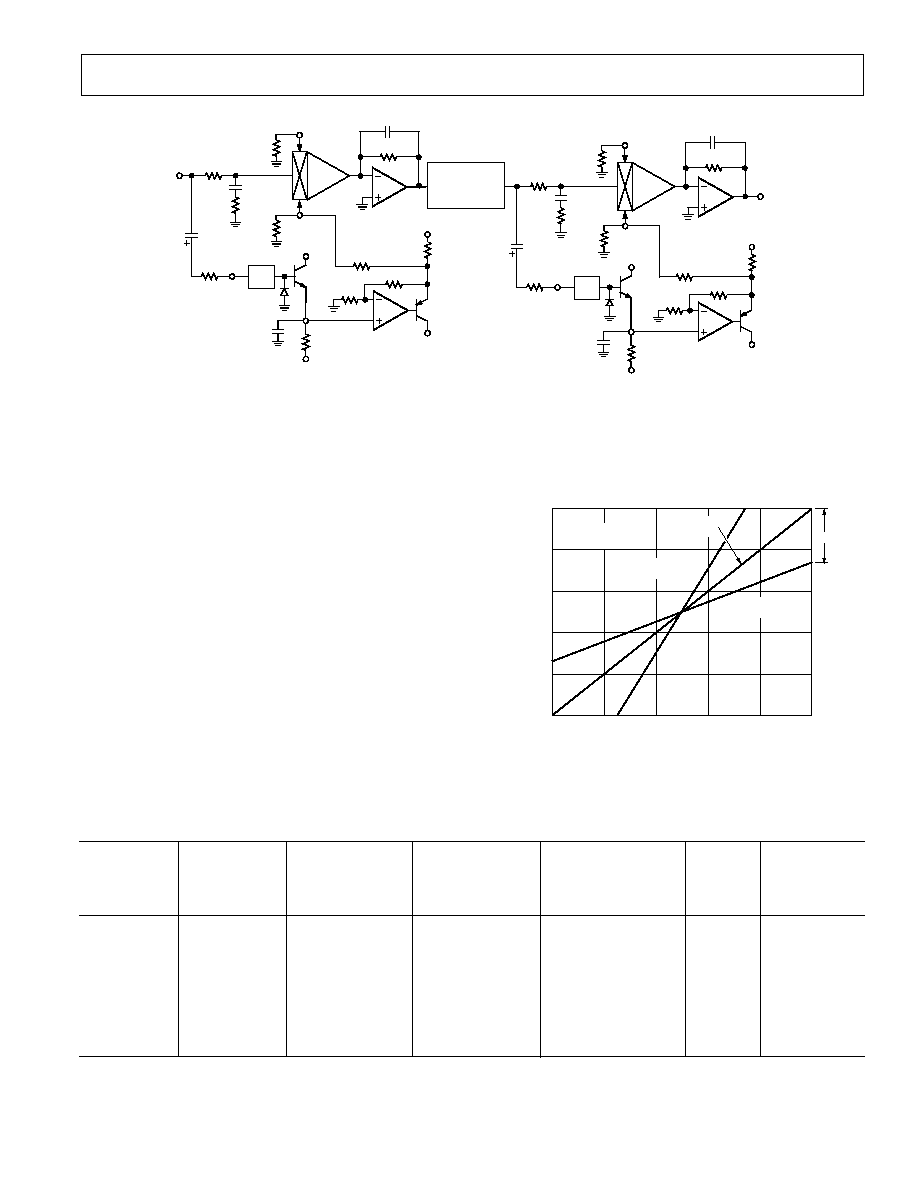
For a positive unipolar control output add two diodes as shown
in Figure 7a. This is useful in compressor/limiter applications.
Figure 7b shows a typical response.
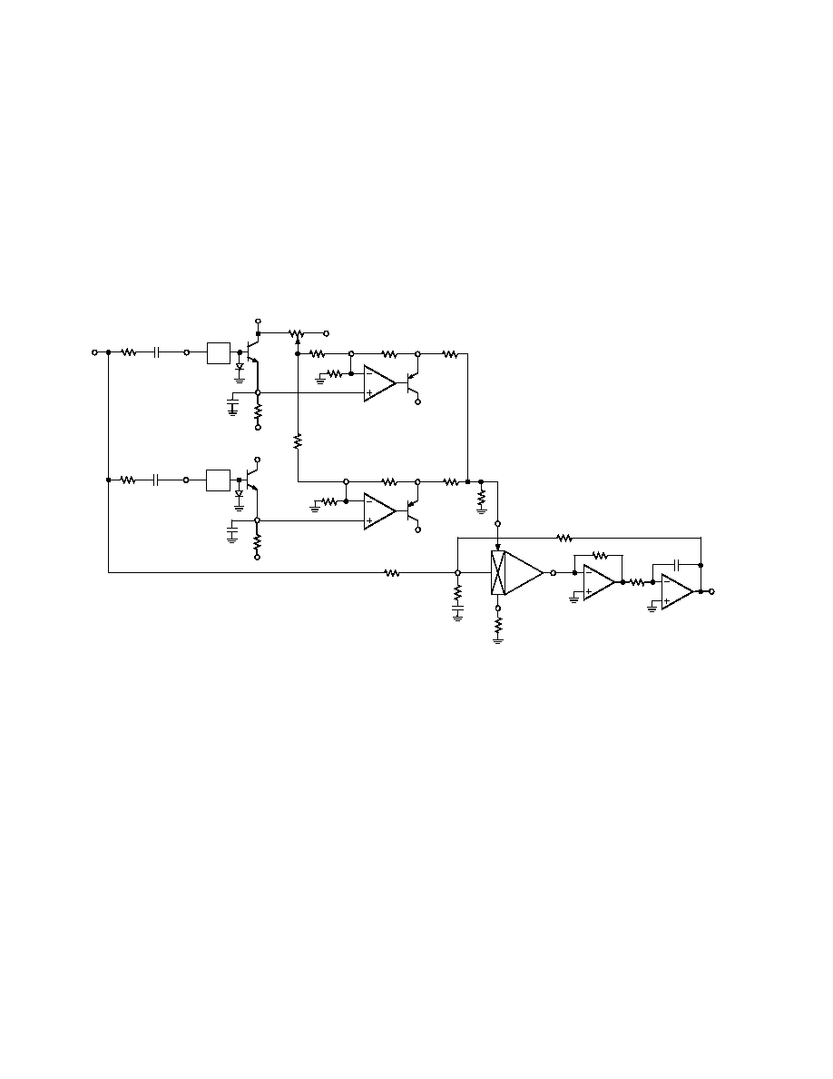
Bipolar control outputs can be realized by adding a resistor from
the op amp output to V+. This is useful in compandor circuits
as shown in Figure 8a, with its response in Figure 8b. The value
of the resistor R
PV
will determine the maximum output from the
control amplifier.
STEREO COMPRESSOR/LIMITER
The two control circuits of Figures 6 and 7 can be used in
conjunction to produce composite control voltages. Figures 9a
and 9b show this type of circuit and transfer function for a
stereo compressor/limiter which also acts as a downward
expander for noise gating. The output noise in the absence of a
V
IN
dB
V
OUT
dB
*
EXPANSION
THRESHOLD
COMPRESSION
THRESHOLD
200
MONO
OR R
L
+V
C
FIGURE 6
200
FIGURE 7
THRESHOLD EXP.
THRESHOLD COM.
V
C
a. Control Circuit b. Input/Output Curve
Figure 9. Control Circuit for Stereo Compressor/Limiter with Noise Gating and Input/Output Curve
V
IN
dB
+
*UPPER LIMIT CAN BE FIXED BY
VALUE OF PULL UP RESISTOR (R
PV
)
CONNECTED TO POSITIVE SUPPLY
THRESHOLD
V
CON
*
2V
|I
I N
|
V+
V+
CON
OUT
REC IN
39k
200
R
CON
TO V
C
R
IN
MONO
OR R
C
AV
R
T
THRESHOLD
CONTROL
LOG AV
R
IN
L
MONO R
IN
= 10k
STEREO R
IN
= 20k
V
1.5M
1k
V
V
T
THRESH
R
PV
a. Control Circuit b. Typical Compressor/Limiter Control
Curve
Figure 7. Compressor/Limiter Control Circuit and Typical Response
*UPPER AND
LOWER LIMITS CAN
BE ESTABLISHED BY
VALUES OF R
PV
AND
R
LL
, RESPECTIVELY
V
IN
dB
+
V
CON
V
T
<
0
V
T
>
0
*
*
V
T
=
0
2V
|I
I N
|
V+
V+
CON
OUT
REC
IN
39k
200
TO +V
C
OR V
C
R
IN
MONO
OR R
C
AV
R
T
GAIN
LOG AV
R
IN
L
MONO R
IN
= 10k
STEREO R
IN
= 20k
V
1.5M
1k
V
V
T
THRESH
R
PV
R
LL
V
a. Control Circuit b. Typical Compandor Control Curves
Figure 8. Compandor Control Circuit and Typical Curves
SSM2120/SSM2122
REV. C
7
V+
LOG AV
V
+V
C
V
C
SIGNAL
INPUT
SIGNAL
OUTPUT
200
2200pF
47
36k
36
10pF
TRANSMISSION
OR
STORAGE
MEDIUM
1µF
|I
I N
|
10k
REC
IN
39k
10k
V+
1k
R
C
1µF
4.7M
V+
LOG AV
V
V
C
+V
C
2200pF
47
36k
36k
10pF
1µF
|I
I N
|
10k
REC
IN
39k
10k
V+
1k
R
E
1µF
4.7M
200
200
200
V
V
Figure 10. Companding Noise Rejection System
signal will be dependent on the noise of the current-to-voltage
converter amplifier if the expansion ratio is high enough.
As discussed in the Threshold Control section, the use of the
control circuit of Figure 6, including the R
PV
to V+ and two
diodes, yields positive unipolar control outputs.
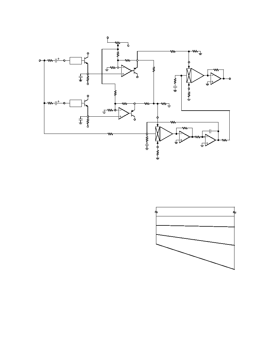
COMPANDING NOISE REDUCTION SYSTEM
A complete companding noise reduction system is shown in
Figure 10. Normally, to obtain an overall gain of unity, the
value of R
C
is equal to R
E
. The values of R
C/E
will determine the
compression/expansion ratio.
Table II shows compression/expansion ratios ranging from 1.5:1
to full limiting with the corresponding values of R
C/E
.
An example of a 2:1 compression/expansion ratio is plotted in
Figure 11. Note that signal compression increases gain for low
level signals and reduces gain for high levels while expansion
does the reverse. The net result for the system is the same as the
original input signal except that it has been compressed before
being sent to a given medium and expanded after recovery. The
compression/expansion ratio needed depends on the medium
being used. As an extreme example, a household tape player
would require a higher compression/expansion ratio than a
professional stereo system.
INPUT SIGNAL LEVEL dB
20
0
80
80
20
60
OUTPUT SIGNAL LEVEL dB
40
20
0
20
40
60
I
REF
3µA
R
REF
= 4.7M
OVERALL
RESPONSE
2:1
EXPANSION
2:1
COMPRESSION
25dB
Figure 11. Companding Noise Reduction with 2:1
Compression/Expansion Ratio
Table II.
Gain
Compressor
Expander
(Reduction
Only
Only
Input Signal
or Increase)
Output Signal
Output Signal
Compression/
V
CONTROL
Increase (dB)
(dB)
Increase (dB)
Increase (dB)
Expansion Ratio
R
C/E
(mV/dB)
20
6.67
13.33
22.67
1.5:1
11,800
2.0
20
10.00
10.00
30.00
2:1
7,800
3.0
20
13.33
6.67
33.33
3:1
5,800
4.0
20
15.00
5.00
35.00
4:1
5,133
4.5
20
16.00
4.00
36.00
5:1
4,800
4.8
20
17.33
2.67
37.33
7.5:1
4,415
5.2
20
18.00
2.00
38.00
10:1
4,244
5.4
20
20.00
0
40.00
AGC*/Limiter
3,800
6.0
*AGC for Compression Only.
SSM2120/SSM2122
REV. C
8
DYNAMIC FILTER
Figure 12 shows a control circuit for a dynamic filter capable of
single ended (nonencode/decode) noise reduction. Such circuits
usually suffer from a loss of high frequency content at low signal
levels because their control circuits detect the absolute amount
of highs present in the signal. This circuit, however, measures
wideband level as well as high frequency band level to produce
a composite control signal combined in a 1:2 ratio respectively.
The upper detector senses wideband signals with a cutoff of
20 Hz while the lower detector has a 5 kHz cutoff to sense only
high frequency band signals. This approach allows very good
noise masking with a minimum loss of "highs" when the signal
level goes below the threshold.
V+
LOG AV
V
AUDIO
INPUT
AUDIO
OUTPUT
160k
2.2µF
|I
I N
|
10k
REC
IN
39k
1.5M
1k
SIG
OUT
3.3µF
+V
C
V
C
2200pF
47
36k
36k
100pF
12k
CON
OUT
V
200
200
9
THRESHOLD
CONTROL
THRESH
3
2
160k
39k
1k
CON
OUT
V
THRESH
14
V+
LOG AV
3300pF
|I
I N
|
10k
REC
IN
1.5M
3.3µF
15
13
F
C
= 5kHz
(HIGH FREQUENCY)
F
C
20Hz
(WIDEBAND)
36k
5
7
SIG
IN
8
5.6k
5
36k
12
1
V
V
Figure 12. Dynamic Noise Filter Circuit

SSM2120/SSM2122
REV. C
9
Figures 13ac show the filter's 3 dB frequency response with the
threshold potentiometer at V+, centered, and V. Data was
taken by applying a 300 Hz signal to the wideband detector and
a 20 kHz signal to the high-frequency band detector simultane-
ously. These figures correspond to filter characteristics for
50 dB, 70 dB and 90 dB dynamic range program source
material, respectively. The system could thus treat signals from
anything ranging from 1/4" magnetic tape to high performance
compact disc players.
Note that in Figure 13a the control circuit is designed so that
the minimum cutoff frequency is about 1 kHz. This occurs as
the control circuit detects the noise floor of the source material.
Dynamic filtering limits the signal bandwidth to less than 1 kHz
unless enough highs are detected in the signal to cover the noise
floor in the mid- and high frequency range. In this case the filter
opens to pass more of the audio band as more highs are detected.
The filter's bandwidth can extend to 50 kHz with a nominal
signal level at the input. At other signal levels with varying high
frequency content, the filter will close to the required band-
width. Here, noise outside the band is removed while the
perceived noise is masked by other signals within the band.
Even in this system, however, a certain amount of mid- and high
frequency components will be lost, especially during transients
at very low signal levels. This circuit does not address low
frequency noise such as "hum" and "rumble."
WIDEBAND SIGNAL LEVEL dB
50
40
30
20
10
0
10
20
20
HIGH-FREQUENCY SIGNAL LEVEL dB
20
30
40
50
0
10
10
1.0
1.0
1.0
1.0
1.0
1.1
1.1
1.1
1.0
1.0
1.2
1.7
2.4
2.4
2.4
1.9
2.75
3.9
5.5
5.5
5.5
6
8.3
11.7
11.7
11.7
17.8
26
26
26
50.6
50.6
50.6
50.6
50.6
50.6
a. V
THRESH
at V+
WIDEBAND SIGNAL LEVEL dB
50
40
30
20
10
0
10
20
20
HIGH-FREQUENCY SIGNAL LEVEL dB
20
30
40
50
0
10
10
1.5
2.2
3.1
4.2
4.2
4.2
4.2
4.2
4.9
7.1
10
10
10
10
10
15.1
22
22
22
22
22
48
49.2
49.2
49.2
49.2
50.6
50.6
50.6
50.6
50.6
50.6
50.6
50.6
50.6
50.6
b. V
THRESH
Centered
WIDEBAND SIGNAL LEVEL dB
50
40
30
20
10
0
10
20
20
HIGH-FREQUENCY SIGNAL LEVEL dB
20
30
40
50
0
10
10
12.3
17.3
17.8
17.8
17.8
17.8
17.8
17.8
40
41
41
41
41
41
41
50.6
50.6
50.6
50.6
50.6
50.6
50.6
50.6
50.6
50.6
50.6
50.6
50.6
50.6
50.6
50.6
50.6
50.6
50.6
50.6
50.6
c. V
THRESH
at V
Figure 13. 3 dB Filter Response
SSM2120/SSM2122
REV. C
10
V+
LOG AV
V
SIGNAL
INPUT
SIGNAL
OUTPUT
160k
IN |I
I N
|
REC
IN
39k
1.5M
1k
C
AV1
V
+V
C
V
C
2200pF
47
36k
36k
100pF
12k
CON
OUT
V
200
200
THRESHOLD
160k
39k
1k
CON
OUT
V
F
C
20Hz
36k
5.6k
36k
R
IN1
V+
V+
LOG AV
IN |I
I N
|
REC
IN
1.5M
C
AV2
V
F
C
= 5Hz
R
IN2
36k
+V
C
V
C
36k
200
200
12k
2200pF
47
DOWNWARD EXPANDER
Figure 14. Dynamic Filter with Downward Expander
DYNAMIC FILTER WITH DOWNWARD EXPANDER
A composite single-ended noise reduction system can be
realized by a combination of dynamic filtering and a downward
expander. As shown in Figure 14, the output from the wideband
detector can also be connected to the +V
C
control port of the
second VCA which is connected in series with the sliding filter.
This will act as a downward expander with a threshold that
tracks that of the filter. Although both of these techniques are
used for noise reduction, each alone will pass appreciable
amounts of noise under some conditions. When used together,
both contribute distinct advantages while compensating for each
other's deficiencies.
Downward expansion uses a VCA controlled by the level
detector. This section maintains dynamic range integrity for all
levels above the user adjustable threshold level. As the input
level decreases below the threshold, gain reduction occurs at an
increasing rate (see Figure 15). This technique reduces audible
noise in fade outs or low level signal passages by keeping the
standing noise floor well below the program material.
This technique by itself is less effective for signals with
predominantly low frequency content such as a bass solo where
wideband frequency noise would be heard at full level. Also,
since the level detector has a time constant for signal averaging,
percussive material can modulate the noise floor causing a
"pumping" or "breathing" effect.
The dynamic filter and downward expander techniques used
together can be employed more subtly to achieve a given level of
noise reduction than would be required if used individually. Up
to 30 dB of noise reduction can be realized while preserving the
crisp highs with a minimum of transient side effects.
+20
30
40
50
60
+20
30
45
60
75
INPUT dB
OUTPUT dB
Figure 15. Typical Downward Expander I/O Characteristics
at 30 dB Threshold Level (1:1.5 Ratio)
SSM2120/SSM2122
REV. C
11
FADER AUTOMATION
The SSM2120 can be used in fader automation systems to serve
two channels. The inverting control port is connected through
an attenuator to the VCA control voltage source. The noninverting
control port is connected to a control circuit (such as Figure 6)
which senses the input signal level to the VCA. Above the
threshold voltage, which can be set quite low (for example
60 dBV), the VCA operates at its programmed gain. Below
this threshold the VCA will downward expand at a rate deter-
mined by the +V
C
control port attenuator. By keeping the release
time constant in the 10 ms to 25 ms range, the modulation of
the VCA standing noise floor (80 dB at unity-gain), can be
kept inaudibly low.
The SSM2300 8-channel multiplexed sample-and-hold IC
makes an excellent controller for VCAs in automation systems.
Figure 16 shows the basic connection for the SSM2122 operating
as a unity-gain VCA with its noninverting control ports grounded
and access to the inverting control ports. This is typical for fader
automation applications. Since this device is a pinout option of
the SSM2120, the VCAs will behave exactly as described
earlier in the VCA section.
The SSM2122 can also be used with two or more op amps to
implement complex voltage-controlled filter functions. Biquad
and state-variable two-pole filters offering low pass, bandpass
and high pass outputs can be realized. Higher order filters can
also be formed by connecting two or more such stages in series.
V
2000pF
47
36k
36k
10pF
1/2
TL082
V+
10pF
0.1µF
+15V
200
SIG
OUT 2
SIG
OUT 1
V
C2
V
C1
SIG
IN 1
1/2
TL082
8
1
2
3
4
7
6
5
14
13
12
11
16
15
10
9
SSM2122
200
220k
200
220k
200
50k
*
150k
V+
36k
V
V+
50k
*
2000pF
47
36k
SIG
IN 2
0.1µF
15V
*
OPTIONAL CONTROL FEEDTHROUGH TRIM
Figure 16. SSM2122 Basic Connection (Control Ports at 0 V)
SSM2120/SSM2122
REV. C
12
C2088211/95
PRINTED IN U.S.A.
OUTLINE DIMENSIONS
Dimensions shown in inches and (mm).
16-Pin Plastic DIP
(N-16)
16
1
8
9
0.840 (21.33)
0.745 (18.93)
0.280 (7.11)
0.240 (6.10)
PIN 1
SEATING
PLANE
0.022 (0.558)
0.014 (0.356)
0.060 (1.52)
0.015 (0.38)
0.210 (5.33)
MAX
0.130
(3.30)
MIN
0.070 (1.77)
0.045 (1.15)
0.100
(2.54)
BSC
0.160 (4.06)
0.115 (2.93)
0.325 (8.25)
0.300 (7.62)
0.015 (0.381)
0.008 (0.204)
0.195 (4.95)
0.115 (2.93)
22-Pin Plastic DIP
(N-22)
22
1
11
12
1.080 (27.43)
1.020 (25.91)
0.280 (7.11)
0.240 (6.10)
PIN 1
SEATING
PLANE
0.022 (0.558)
0.014 (0.356)
0.060 (1.52)
0.015 (0.38)
0.210
(5.33)
MAX
0.070 (1.77)
0.045 (1.15)
0.100
(2.54)
BSC
0.160 (4.06)
0.115 (2.93)
0.325 (8.25)
0.300 (7.62)
0.015 (0.381)
0.008 (0.204)
0.195 (4.95)
0.115 (2.93)