 | ÐлекÑÑоннÑй компоненÑ: SSM2135 | СкаÑаÑÑ:  PDF PDF  ZIP ZIP |
Äîêóìåíòàöèÿ è îïèñàíèÿ www.docs.chipfind.ru
PIN CONNECTIONS
REV. D
Information furnished by Analog Devices is believed to be accurate and
reliable. However, no responsibility is assumed by Analog Devices for its
use, nor for any infringements of patents or other rights of third parties
which may result from its use. No license is granted by implication or
otherwise under any patent or patent rights of Analog Devices.
a
Dual Single-Supply
Audio Operational Amplifier
SSM2135
One Technology Way, P.O. Box 9106, Norwood, MA 02062-9106, U.S.A.
Tel: 617/329-4700
Fax: 617/326-8703
FEATURES
Excellent Sonic Characteristics
High Output Drive Capability
5.2 nV/
Hz Equivalent Input Noise @ 1 kHz
0.001% THD+N (V
O
= 2.5 V p-p @ 1 kHz)
3.5 MHz Gain Bandwidth
Unity-Gain Stable
Low Cost
APPLICATIONS
Multimedia Audio Systems
Microphone Preamplifier
Headphone Driver
Differential Line Receiver
Balanced Line Driver
Audio ADC Input Buffer
Audio DAC l-V Converter and Filter
Pseudo-Ground Generator
GENERAL DESCRIPTION
The SSM2135 Dual Audio Operational Amplifier permits
excellent performance in portable or low power audio systems,
with an operating supply range of +4 V to +36 V or
±
2 V to
±
18 V. The unity gain stable device has very low voltage noise
of 4.7 nV/
Hz, and total harmonic distortion plus noise below
0.01% over normal signal levels and loads. Such characteristics
are enhanced by wide output swing and load drive capability. A
unique output stage* permits output swing approaching the rail
under moderate load conditions. Under severe loading, the
SSM2135 still maintains a wide output swing with ultralow
distortion.
Particularly well suited for computer audio systems and
portable digital audio units, the SSM2135 can perform
preamplification, headphone and speaker driving, and balanced
line driving and receiving. Additionally, the device is ideal for
input signal conditioning in single-supply sigma-delta analog-
to-digital converter subsystems such as the AD1878/AD1879.
The SSM2135 is available in 8-lead plastic DIP and SOIC
packages, and is guaranteed for operation over the extended
industrial temperature range of 40
°
C to +85
°
C.
*Protected by U. S. Patent No. 5,146,181.
SSM2135
V+
OUT B
IN B
+IN B
OUT A
IN A
+IN A
V/GND
SSM2135
OUT A
IN A
+IN A
V/GND
1
2
3
4
8
7
6
5
V+
OUT B
IN B
+IN B
(S Suffix)
(P-Suffix)
8-Lead Narrow-Body SOIC
8-Lead Epoxy DIP
FUNCTIONAL BLOCK DIAGRAM
9V 9V
+IN
IN
OUT
V+
V/GND
REV. D
2
SSM2135SPECIFICATIONS
Parameter
Symbol
Conditions
Min
Typ
Max
Units
AUDIO PERFORMANCE
Voltage Noise Density
e
n
f = 1 kHz
5.2
nV/
Hz
Current Noise Density
i
n
f = 1 kHz
0.5
pA/
Hz
Signal-To-Noise Ratio
SNR
20 Hz to 20 kHz, 0 dBu = 0.775 V rms
121
dBu
Headroom
HR
Clip Point = 1% THD+N, f = 1 kHz, R
L
= 10 k
5.3
dBu
Total Harmonic Distortion
THD+N
A
V
= +1, V
O
= 1 V p-p, f = 1 kHz, 80 kHz LPF
R
L
= 10 k
0.003
%
R
L
= 32
0.005
%
DYNAMIC PERFORMANCE
Slew Rate
SR
R
L
= 2 k
, T
A
= +25
°
C
0.6
0.9
V/
µ
s
Gain Bandwidth Product
GBW
3.5
MHz
Settling Time
t
S
to 0.1%, 2 V Step
5.8
µ
s
INPUT CHARACTERISTICS
Input Voltage Range
V
CM
0
+4.0
V
Input Offset Voltage
V
OS
V
OUT
= 2 V
0.2
2.0
mV
Input Bias Current
I
B
V
CM
= 0 V, V
OUT
= 2 V
300
750
nA
Input Offset Current
I
OS
V
CM
= 0 V, V
OUT
= 2 V
50
nA
Differential Input Impedance
Z
IN
4
M
Common-Mode Rejection
CMR
0 V
V
CM
4 V, f = dc
87
112
dB
Large Signal Voltage Gain
A
VO
0.01 V
V
OUT
3.9 V, R
L
= 600
2
V/
µ
V
OUTPUT CHARACTERISTICS
Output Voltage Swing High
V
OH
R
L
= 100 k
4.1
V
R
L
= 600
3.9
V
Output Voltage Swing Low
V
OL
R
L
= 100 k
3.5
mV
R
L
= 600
3.0
mV
Short Circuit Current Limit
I
SC
±
30
mA
POWER SUPPLY
Supply Voltage Range
V
S
Single Supply
+4
+36
V
Dual Supply
±
2
±
18
V
Power Supply Rejection Ratio
PSRR
V
S
= +4 V to +6 V, f = dc
90
120
dB
Supply Current
I
SY
V
OUT
= 2.0 V, No Load
V
S
= +5 V
2.8
6.0
mA
V
S
=
±
18 V, V
OUT
= 0 V, No Load
3.7
7.6
mA
(V
S
= +5 V, 40 C < T
A
< +85 C unless otherwise noted.
Typical specifications apply at T
A
= +25 C.)
ABSOLUTE MAXIMUM RATINGS
Supply Voltage
Single Supply . . . . . . . . . . . . . . . . . . . . . . . . . . . . . . . +36 V
Dual Supply . . . . . . . . . . . . . . . . . . . . . . . . . . . . . . . .
±
18 V
Input Voltage . . . . . . . . . . . . . . . . . . . . . . . . . . . . . . . . . . .
±
V
S
Differential Input Voltage . . . . . . . . . . . . . . . . . . . . . . . . 10 V
Output Short Circuit Duration . . . . . . . . . . . . . . . . Indefinite
Storage Temperature Range . . . . . . . . . . . . 65
°
C to +150
°
C
Operating Temperature Range . . . . . . . . . . . 40
°
C to +85
°
C
Junction Temperature Range (T
J
) . . . . . . . . 65
°
C to +150
°
C
Lead Temperature (Soldering, 60 sec) . . . . . . . . . . . . +300
°
C
ESD RATINGS
883 (Human Body) Model . . . . . . . . . . . . . . . . . . . . . . . 1 kV
EIAJ Model . . . . . . . . . . . . . . . . . . . . . . . . . . . . . . . . . . 175 V
THERMAL CHARACTERISTICS
Thermal Resistance
1
8-Lead Plastic DIP
JA
103
°
C/W
JC
43
°
C/W
8-Lead SOIC
JA
158
°
C/W
JC
43
°
C/W
1
JA
is specified for worst case conditions, i.e.,
JA
is specified for device in
socket for P-DIP and device soldered in circuit board for SOIC package.
ORDERING GUIDE
Temperature
Package
Package
Model
Range
Description
Option
SSM2135P
40
°
C to +85
°
C
8-Lead Plastic DIP N-8
SSM2135S
40
°
C to +85
°
C
8-Lead SOIC
SO-8
SSM2135
REV. D
3
+5V
+2.5Vdc
R
L
500
µ
F
+
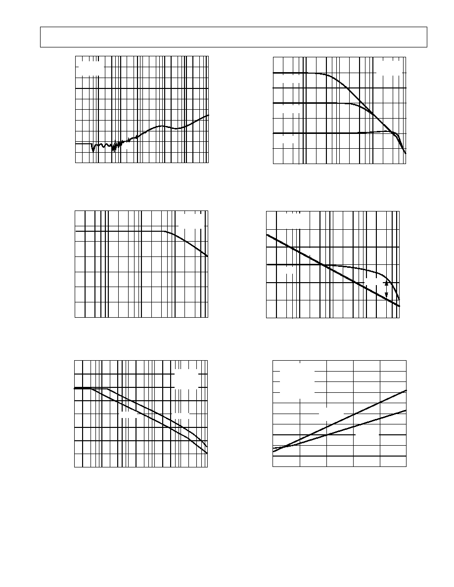
Figure 1. Test Circuit for Figures 24
Figure 2. THD+N vs. Amplitude (See Test Circuit; A
V
= +1,
V
S
= +5 V, f = 1 kHz, with 80 kHz Low-Pass Filter)
Figure 3. THD+N vs. Frequency (See Test Circuit;
A
V
= +1, V
IN
= 1 V p-p, with 80 kHz Low-Pass Filter)
10
0.1
0.001
10
100
10k
1k
1
0.01
LOAD RESISTANCE
THD %
V
S
=
+5V
A
V
=
+1,
= 1kHz
V
IN
=
1Vp-p
R
L
=
10k
WITH 80kHz FILTER
Figure 4. THD+N vs. Load (See Test Circuit)
1
0.001
0
20
60
40
0.01
10
0.1
30
50
V
S
=
+5V
R
L
=
100k
V
OUT
=
2.5Vp-p
= 1kHz
WITH 80kHz FILTER
GAIN dB
THD+N %
NONINVERTING
INVERTING
Figure 5. THD+N vs. Gain
1
0.01
0.001
10
30
20
0.1
SUPPLY VOLTAGE V
THD+N %
V
S
=
+5V
A
V
=
+1,
= 1kHz
V
IN
=
1Vp-p
R
L
=
10k
WITH 80kHz FILTER
5
15
25
Figure 6. THD+N vs. Supply Voltage
SSM2135
REV. D
4
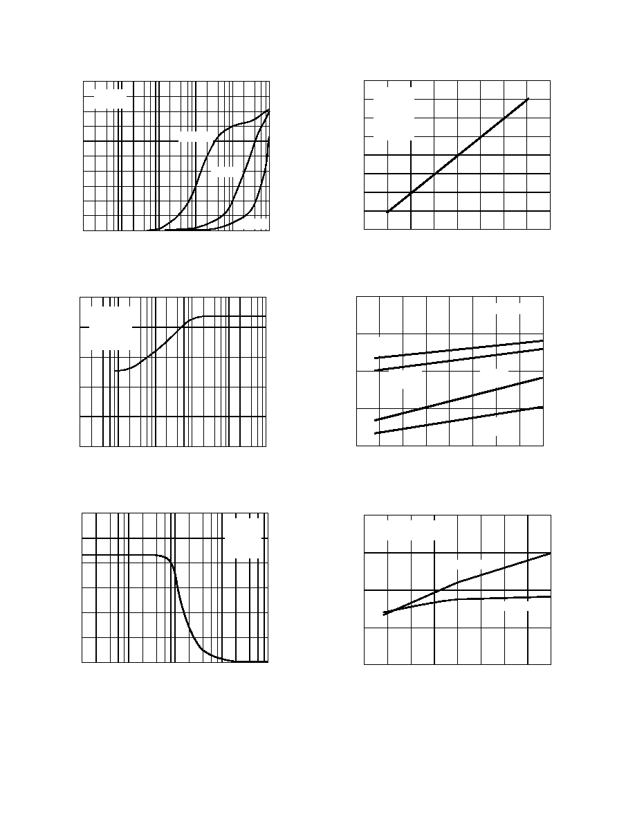
Figure 7. SMPTE Intermodulation Distortion (A
V
= +1,
V
S
= +5 V, f = 1 kHz, R
L
= 10 k
)
10
0%
100
90
1s
Figure 8. Input Voltage Noise (20 nV/div)
30
15
0
1
10
1k
100
5
20
25
FREQUENCY Hz
V
S
= +5V
T
A
= +25
°
C
10
e
n
nV/
Hz
Figure 9. Voltage Noise Density vs. Frequency
5
2
0
1
10
1k
100
1
3
4
FREQUENCY Hz
V
S
= +5V
T
A
= +25
°
C
i
n
pA/
Hz
Figure 10. Current Noise Density vs. Frequency
Figure 11. Frequency Response (A
V
= +1, V
S
= +5 V,
V
IN
= 1 V p-p, R
L
= 10 k
)
10
100
0%
90
1
µ
S
500m V
Figure 12. Square Wave Response (V
S
= +5 V, A
V
= +1,
R
L
=
)
SSM2135
REV. D
5
10
100
10M
1M
100k
10k
1k
FREQUENCY Hz
105
60
40
20
0
20
40
60
80
100
120
CHANNEL SEPARATION dB
V
S
= +5V
T
A
= +25
°
C
Figure 13. Crosstalk vs. Frequency (R
L
= 10 k
)
140
100
0
1k
1M
100k
10k
100
120
60
80
20
40
FREQUENCY Hz
COMMON-MODE REJECTION dB
V
S
= +5V
T
A
= +25
°
C
Figure 14. Common-Mode Rejection vs. Frequency
140
60
20
10
100
1M
100k
10k
1k
80
100
120
0
20
40
FREQUENCY Hz
V
S
= +5V
A
V
= +1
T
A
= +25
°
C
PSRR dB
+PSRR
PSRR
Figure 15. Power Supply Rejection vs. Frequency
50
30
20
10k
10M
1M
100k
1k
40
10
20
10
0
FREQUENCY Hz
CLOSED-LOOP GAIN dB
V
S
= +5V
T
A
= +25
°
C
A
V
= +100
A
V
= +10
A
V
= +1
Figure 16. Closed-Loop Gain vs. Frequency
100
40
20
10k
10M
1M
100k
1k
20
0
60
80
FREQUENCY Hz
OPEN-LOOP GAIN dB
90
225
135
180
45
0
PHASE Degrees
V
S
= +5V
T
A
= +25
°
C
GAIN
PHASE
m = 57
°
Figure 17. Open-Loop Gain and Phase vs. Frequency
50
0
500
15
5
100
10
0
30
20
25
35
40
45
400
300
200
LOAD CAPACITANCE pF
OVERSHOOT %
NEGATIVE
EDGE
POSITIVE
EDGE
V
S
= +5V
R
L
= 2k
V
IN
= 100mVpp
T
A
= +25
°
C
A
V
= +1
Figure 18. Small Signal Overshoot vs. Load Capacitance
SSM2135
REV. D
6
FREQUENCY Hz
50
25
0
10
100
1M
100k
10k
1k
30
35
40
45
5
10
15
20
V
S
= +5V
T
A
= +25
°
C
IMPEDANCE
A
VCL
= +100
A
VCL
= +1
A
VCL
= +10
Figure 19. Output Impedance vs. Frequency
5
4
0
1
10
100k
10k
1k
100
3
2
1
V
S
= +5V
T
A
= +25
°
C
A
V
= +1
= 1kHz
THD+N = 1%
LOAD RESISTANCE
MAXIMUM OUTPUT Volts
Figure 20. Maximum Output Voltage vs. Load Resistance
6
3
0
10k
10M
1M
100k
1k
2
1
4
5
FREQUENCY Hz
MAXIMUM OUTPUT SWING Volts
V
S
= +5V
R
L
= 2k
T
A
= +25
°
C
A
V
= +1
Figure 21. Maximum Output Swing vs. Frequency
40
20
0
0
5
40
35
30
25
20
15
10
25
30
35
5
10
15
V
S
= +5V
A
V
= +1
R
L
= 10k
= 1kHz
THD+N = 1%
T
A
= +25
°
C
SUPPLY VOLTAGE Volts
OUTPUT VOLTAGE Volts
Figure 22. Output Swing vs. Supply Voltage
5.0
3.0
125
4.5
3.5
50
4.0
75
100
50
25
0
25
TEMPERATURE
°
C
POSITIVE OUTPUT SWING Volts
V
S
= +5.0V
2.0
0
1.5
0.5
1.0
NEGATIVE OUTPUT SWING Volts
+SWING
R
L
= 2k
+SWING
R
L
= 600
SWING
R
L
= 2k
SWING
R
L
= 600
75
Figure 23. Output Swing vs. Temperature and Load
2.0
0
125
1.5
0.5
50
1.0
75
100
50
25
0
25
TEMPERATURE
°
C
SLEW RATE V/
µ
s
V
S
= +5V
+0.5V
V
OUT
+4.0V
SLEW RATE
+SLEW RATE
75
Figure 24. Slew Rate vs. Temperature
SSM2135
REV. D
7
5
0
125
3
1
50
2
4
100
75
50
25
0
25
TEMPERATURE
°
C
SUPPLY CURRENT mA
V
S
=
±
18V
V
S
=
±
15V
V
S
= +5.0V
75
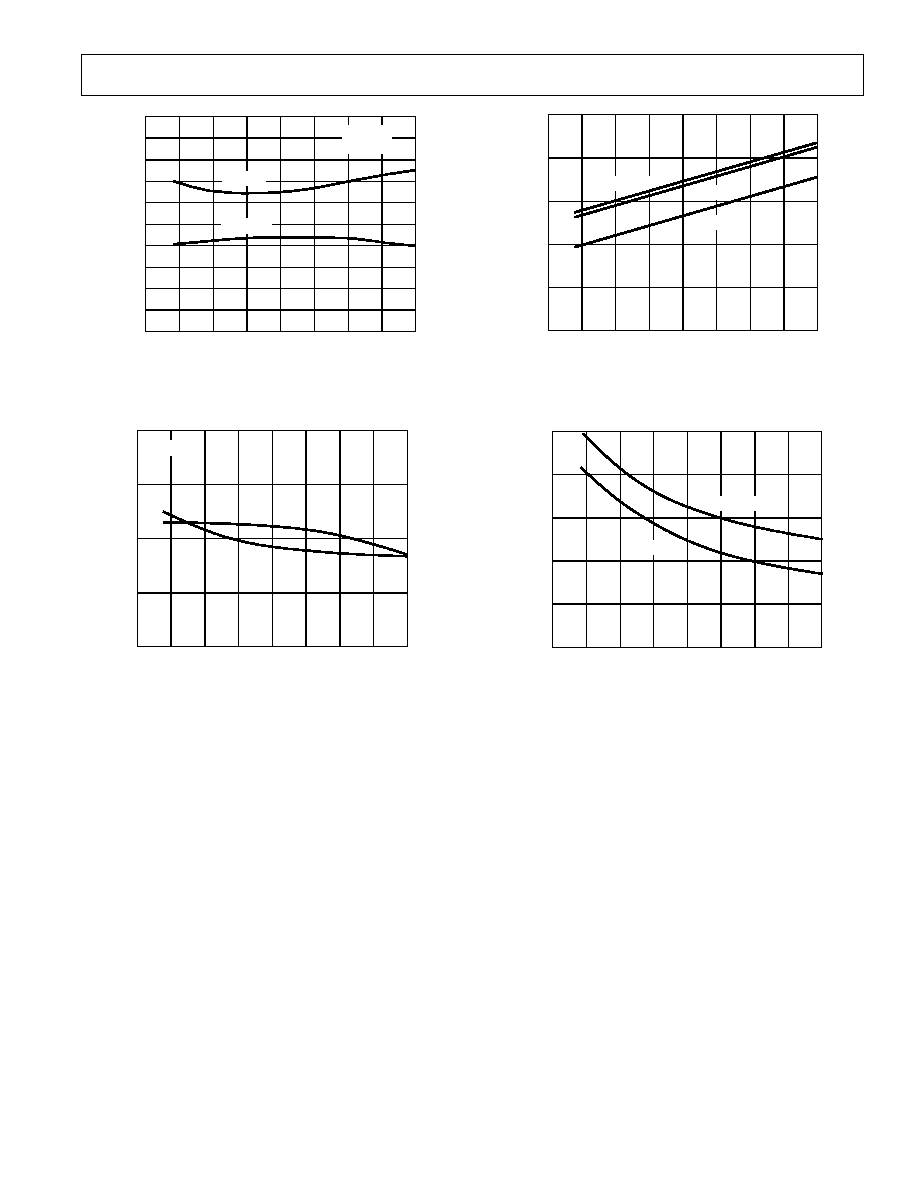
Figure 27. Supply Current vs. Temperature
500
0
125
300
100
50
200
400
100
75
50
25
0
25
TEMPERATURE
°
C
INPUT BIAS CURRENT nA
V
S
=
±
15V
V
S
= +5.0V
75
Figure 28. Input Bias Current vs. Temperature
20
0
125
6
2
50
4
12
8
10
14
16
18
100
75
50
25
0
25
TEMPERATURE
°
C
OPEN-LOOP GAIN V/
µ
V
R
L
= 2k
R
L
= 600
V
S
= +5.0V
V
O
= 3.9V
75
Figure 25. Open-Loop Gain vs. Temperature
70
50
125
65
55
50
60
75
100
50
25
0
25
TEMPERATURE
°
C
PHASE MARGIN Degrees
V
S
= +5V
5
1
4
2
3
GAIN-BANDWIDTH PRODUCT MHz
75
GBW
m
Figure 26. Gain Bandwidth Product and Phase Margin vs.
Temperature
APPLICATION INFORMATION
The SSM2135 is a low voltage audio amplifier that has
exceptionally low noise and excellent sonic quality even when
driving loads as small as 25
. Designed for single supply use,
the SSM2135's inputs common-mode and output swing to zero
volts. Thus with a supply voltage at +5 V, both the input and
output will swing from 0 V to +4 V. Because of this, signal
dynamic range can be optimized if the amplifier is biased to a
+2 V reference rather than at half the supply voltage.
The SSM2135 is unity-gain stable, even when driving into a fair
amount of capacitive load. Driving up to 500 pF does not cause
any instability in the amplifier. However, overshoot in the
frequency response increases slightly.
The SSM2135 makes an excellent output amplifier for +5 V
only audio systems such as a multimedia workstation, a CD
output amplifier, or an audio mixing system. The amplifier has
large output swing even at this supply voltage because it is
designed to swing to the negative rail. In addition, it easily
drives load impedances as low as 25
with low distortion.
The SSM2135 is fully protected from phase reversal for inputs
going to the negative supply rail. However, an internal ESD
protection diodes will turn "on" when either input is forced
more than 0.5 V below the negative rail. Under this condition,
input current in excess of 2 mA may cause erratic output
behavior, in which case a current limiting resistor should be
included in the offending input if phase integrity is required
with excessive input voltages. A 500
or higher series input
resistor will prevent phase inversion even with the input pulled 1
volt below the negative supply.
"Hot" plugging the input to a signal generally does not present a
problem for the SSM2135, assuming the signal does not have
any voltage exceeding the device's supply voltage. If so, it is
advisable to add a series input resistor to limit the current, as
well as a Zener diode to clamp the input to a voltage no higher
than the supply.
SSM2135
REV. D
8
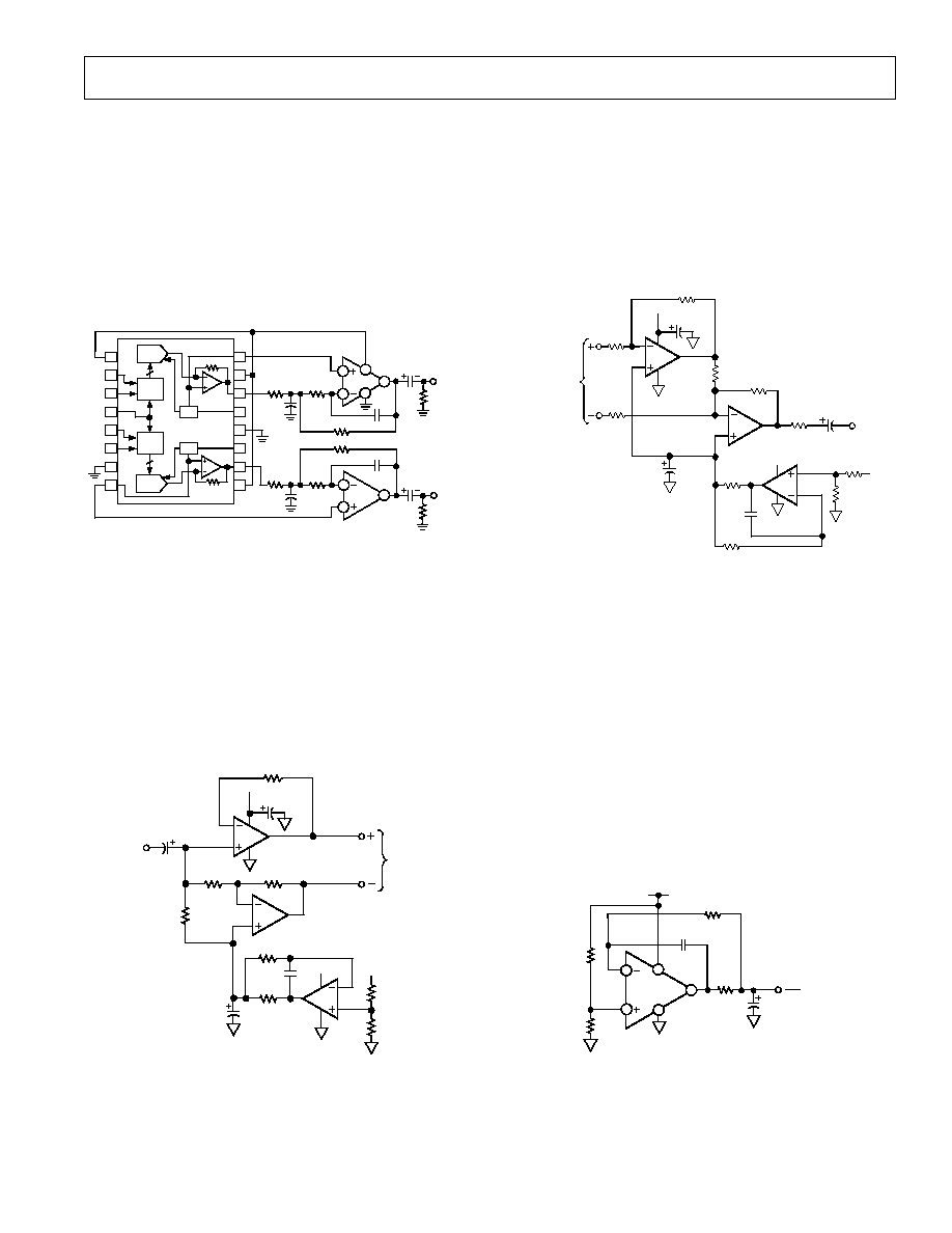
APPLICATION CIRCUITS
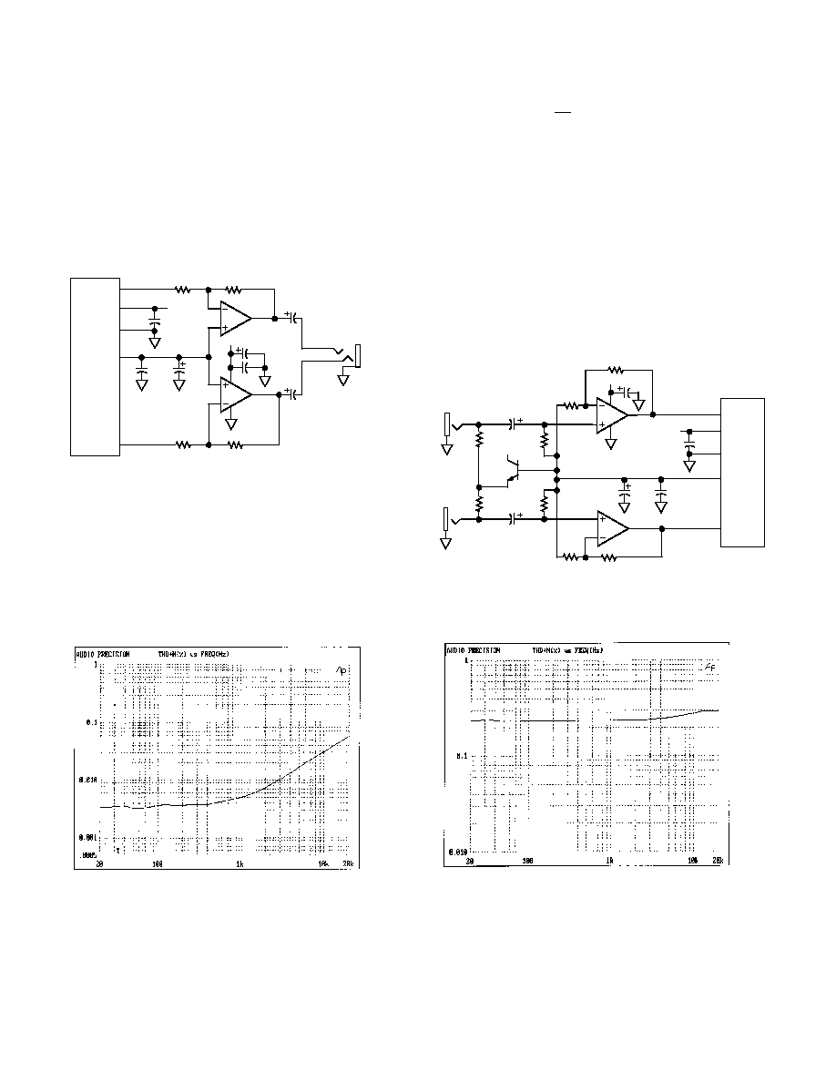
A Low Noise Stereo Headphone Driver Amplifier
Figure 29 shows the SSM2135 used in a stereo headphone
driver for multimedia applications with the AD1848, a 16-bit
stereo codec. The SSM2135 is equally well suited for the serial-
bused AD1849 stereo codec. The headphone's impedance can
be as low as 25
, which covers most commercially available high
fidelity headphones. Although the amplifier can operate at up to
±
18 V supply, it is just as efficient powered by a single +5 V. At
this voltage, the amplifier has sufficient output drive to deliver
distortion-free sound to a low impedance headphone.
10µF
4
6
5
8
7
0.1µF
1/2
SSM2135
10µF
+5V
1/2
SSM2135
0.1µF
1
2
3
8.66k
10k
0.1µF
40
35/36
32
41
L CH
R CH
AGND
34/37
8.66k
10k
V
CC
GND
V
REF
R
OUT
AD1848
L
OUT
470µF
470µF
Figure 29. A Stereo Headphone Driver for Multimedia
Sound Codec
Figure 30 shows the total harmonic distortion characteristics
versus frequency driving into a 32
load, which is a very typical
impedance for a high quality stereo headphone. The SSM2135
has excellent power supply rejection, and as a result, is tolerant
of poorly regulated supplies. However, for best sonic quality, the
power supply should be well regulated and heavily bypassed to
minimize supply modulation under heavy loads. A minimum of
10
µ
F bypass is recommended.
Figure 30. Headphone Driver THD+N vs. Frequency into a
32
Load (V
S
= +5 V, with 80 kHz Low-Pass Filter)
A Low Noise Microphone Preamplifier
The SSM2135's 4.7 nV/
Hz input noise in conjunction with
low distortion makes it an ideal device for amplifying low level
signals such as those produced by microphones. Figure 31 illus-
trates a stereo microphone input circuit feeding a multimedia
sound codec. As shown, the gain is set at 100 (40 dB), although
it can be set to other gains depending on the microphone output
levels. Figure 32 shows the preamplifier's harmonic distortion
performance with 1 V rms output while operating from a single
+5 V supply.
The SSM2135 is biased to 2.25 V by the V
REF
pin of the
AD1848 codec. The same voltage is buffered by the 2N4124
transistor to provide "phantom power" to the microphone. A
typical electret condenser microphone with an impedance range
of 100
to 1 k
works well with the circuit. This power booster
circuit may be omitted for dynamic microphone elements.
L CHANNEL
MIC IN
10µF
4
6
5
8
7
10µF
1/2
SSM2135
10µF
+5V
1/2
SSM2135
0.1µF
1
2
3
10k
10k
100
R CHANNEL
MIC IN
100
0.1µF
29
35/36
34/37
+5V
LMIC
V
CC
GND
V
REF
RMIC
AD1848
32
28
10k
10k
+5V
2N4124
10µF
2k
2k
Figure 31. Low Noise Microphone Preamp for Multimedia
Sound Codec
Figure 32. MIC Preamp THD+N Performance (V
S
= +5 V,
A
V
= 40 dB, V
OUT
= 1 V rms, with 80 kHz Low-Pass Filter)
SSM2135
REV. D
9
An 18-Bit Stereo CD-DAC Output Amplifier
The SSM2135 makes an ideal single supply stereo output
amplifier for audio D/A converters because of its low noise and
distortion. Figure 33 shows the implementation of an 18-bit ste-
reo DAC channel. The output amplifier also provides low-pass
filtering for smoothing the oversampled audio signal. The filter's
cutoff frequency is set at 22.5 kHz and it has a maximally flat
response from dc to 20 kHz.
As mentioned above, the amplifier's outputs can drive directly
into a stereo headphone that has impedance as low as 25
with
no additional buffering required.
6
7
5
100pF
330pF
16
15
14
13
12
11
10
9
18-BIT
DAC
V
REF
18-BIT
SERIAL
REG.
VOL
AGND
18-BIT
SERIAL
REG.
18-BIT
DAC
V
REF
VOR
VBL
DGND
VBR
LR
DR
LL
DL
CK
V
L
V
S
1
2
3
4
5
6
7
8
AD1868
220
µ
F
47k
RIGHT
CHANNEL
OUTPUT
330pF
100pF
220
µ
F
LEFT
CHANNEL
OUTPUT
+5V SUPPLY
1
3
2
4
8
1/2
SSM2135
1/2
SSM2135
47k
7.68k
7.68k
7.68k
7.68k
9.76k
9.76k
Figure 33. +5 V Stereo 18-Bit DAC
A Single Supply Differential Line Driver
Signal distribution and routing is often required in audio
systems, particularly portable digital audio equipment for
professional applications. Figure 34 shows a single supply line
driver circuit that has differential output. The bottom amplifier
provides a 2 V dc bias for the differential amplifier in order to
maximize the output swing range. The amplifier can output a
maximum of 0.8 V rms signal with a +5 V supply. It is capable
of driving into 600
line termination at a reduced output
amplitude.
1µF
6
5
8
7
1/2
SSM2135
0.1µF
100
1/2
SSM2135
1
2
3
10µF+0.1µF
+5V
4
1k
8
1
3
2
4
DIFFERENTIAL
AUDIO OUT
2.5k
7.5k
5k
+5V
10k
2.0V
1k
+5V
1/2
SSM2135
1k
100µF
AUDIO
IN
Figure 34. Single Supply Differential Line Driver
A Single Supply Differential Line Receiver
Receiving a differential signal with minimum distortion is
achieved using the circuit in Figure 35. Unlike a difference
amplifier (a subtractor), the circuit has a true balanced input
impedance regardless of input drive levels. That is, each input
always presents a 20 k
impedance to the source. For best
common-mode rejection performance, all resistors around the
differential amplifier must be very well matched. Best results
can be achieved using a 10 k
precision resistor network.
1µF
6
5
8
7
1/2
SSM2135
10µF
+5V
0.1µF
20k
1/2
SSM2135
1
2
3
10µF+0.1µF
+5V
4
2.0V
1/2
SSM2135
DIFFERENTIAL
AUDIO IN
8
1
3
2
4
+5V
2.5k
AUDIO
OUT
20k
20k
10k
10k
100
5k
7.5k
10
Figure 35. Single Supply Balanced Differential Line
Receiver
A Pseudo-Reference Voltage Generator
For single supply circuits, a reference voltage source is often
required for biasing purposes or signal offsetting purposes. The
circuit in Figure 36 provides a supply splitter function with low
output impedance. The 1
µ
F output capacitor serves as a charge
reservoir to handle a sudden surge in demand by the load as
well as providing a low ac impedance to it. The 0.1
µ
F feedback
capacitor compensates the amplifier in the presence of a heavy
capacitive load, maintaining stability.
The output can source or sink up to 12 mA of current with
+5 V supply, limited only by the 100
output resistor. Reduc-
ing the resistance will increase the output current capability.
Alternatively, increasing the supply voltage to 12 V also
improves the output drive to more than 25 mA.
C1
0.1µF
R2
5k
C2
1µF
R4
100
OUTPUT
V
S
+
2
1/2
SSM2135
1
8
4
2
R3
2.5k
3
R1
5k
V
S
+
= +5V
+12V
Figure 36. Pseudo-Reference Generator
SSM2135
REV. D
10
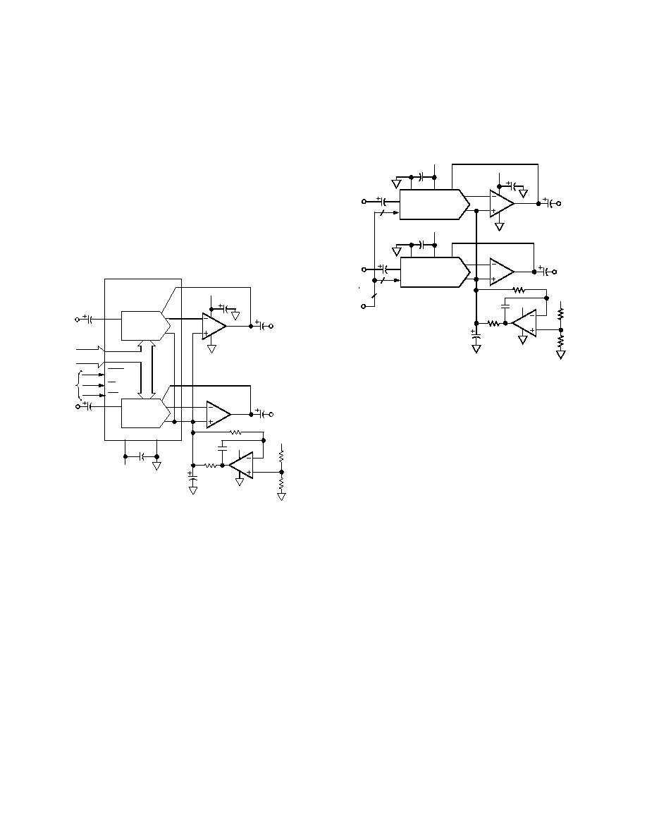
A Digital Volume Control Circuit
Working in conjunction with the AD7528/PM7528 dual 8-bit
D/A converter, the SSM2135 makes for an efficient audio
attenuator, as shown in Figure 37. The circuit works off a single
+5 V supply. The DAC's are biased to a 2 V reference level
which is sufficient to keep the DAC's internal R-2R ladder
switches operating properly. This voltage is also the optimal
midpoint of the SSM2135's common-mode and output swing
range. With the circuit as shown, the maximum input and
output swing is 1.25 V rms. Total harmonic distortion measures
a respectable 0.01% at 1 kHz and 0.1% at 20 kHz. The fre-
quency response at any attenuation level is flat to 20 kHz.
Each DAC can be controlled independently via the 8-bit parallel
data bus. The attenuation level is linearly controlled by the
binary weighting of the digital data input. Total attenuation
ranges from 0 dB to 48 dB.
1µF
47µF
8
47µF
2k
100
0.1µF
1/2
SSM2135
1
2
3
10µF+0.1µF
+5V
4
1/2
SSM2135
8
1
3
2
4
+5V
5k
L AUDIO
OUT
47µF
1/2
SSM2135
R AUDIO
OUT
6
5
7
2.0V
7.5k
+5V
2.0V
3
2
19
20
1
17
5
18
4
6
15
16
DACA/
DACB
CS
WR
REF B
DAC B
FB
OUTB
V
DD
DGND
0.1µF
+5V
47µF
L AUDIO
IN
DATA IN
CONTROL
SIGNAL
R AUDIO
IN
AD/PM-7528
REF A
DAC A
FB
OUTA
Figure 37. Digital Volume Control
A Logarithmic Volume Control Circuit
Figure 38 shows a logarithmic version of the volume control
function. Similar biasing is used. With an 8-bit bus, the
AD7111 provides an 88.5 dB attenuation range. Each bit
resolves a 0.375 dB attenuation. Refer to AD7111 data sheet for
attenuation levels for each input code.
1µF
8
47µF
2k
100
0.1µF
1/2
SSM2135
1
2
3
4
1/2
SSM2135
8
1
3
2
4
+5V
5k
L AUDIO
OUT
47µF
1/2
SSM2135
R AUDIO
OUT
6
5
7
7.5k
+5V
2.0V
0.1µF
+5V
L AUDIO
IN
DATA IN &
CONTROL
R AUDIO
IN
10µF+0.1µF
+5V
1
2
15
3
14
16
47µF
DGND
AD7111
FB
OUTA
V
DD
AGND
V
IN
1
2
0.1µF
+5V
3
14
16
DGND
AD7111
FB
OUTA
V
DD
AGND
V
IN
15
47µF
10
10
10
Figure 38. Single Supply Logarithmic Volume Control

SSM2135
REV. D
11
SPICE MACROMODEL
*
SSM2135 SPICE Macro-Model
9/92, Rev. A
*
JCB/ADI
*Copyright 1993 by Analog Devices, Inc.
*
*Node Assignments
*
*
Noninverting Input
*
Inverting Input
*
Positive Supply
*
Negative Supply
*
Output
.SUBCKT SSM2135
3
2
7
4
6
*
* INPUT STAGE
R3
4
19
1.5E3
R4
4
20
1.5E3
C1
19
20
5.311E12
I1
7
18
106E6
IOS
2
3
25E09
EOS
12
5
POLY(1)
51
4
25E06
1
Q1
19
3
18
PNP1
Q2
20
12
18
PNP1
CIN
3
2
3E12
D1
3
1
DY
D2
2
1
DY
EN
5
2
22
0
1
GN1
0
2
25
0
1E5
GN2
0
3
28
0
1E5
*
* VOLTAGE NOISE SOURCE WITH FLICKER NOISE
DN1
21
22
DEN
DN2
22
23
DEN
VN1
21
0
DC 2
VN2
0
23
DC 2
*
* CURRENT NOISE SOURCE WITH FLICKER NOISE
DN3
24
25
DIN
DN4
25
26
DIN
VN3
24
0
DC 2
VN4
0
26
DC 2
*
* SECOND CURRENT NOISE SOURCE
DN5
27
28
DIN
DN6
28
29
DIN
VN5
27
0
DC 2
VN6
0
29
DC 2
*
* GAIN STAGE & DOMINANT POLE AT .2000E+01 HZ
G2
34
36
19
20
2.65E04
R7
34
36
39E+06
V3
35
4
DC
6
D4
36
35
DX
VB2
34
4
1.6
*
* SUPPLY/2 GENERATOR
ISY
7
4
0.2E3
R10
7
60
40E+3
R11
60
4
40E+3
C3
60
0
1E9
*
* CMRR STAGE & POLE AT 6 kHZ
ECM
50
4
POLY(2)
3
60
2
60
0
1.6 1.6
CCM
50
51
26.5E12
RCM1
50
51
1E6
RCM2
51
4
1
*
*
OUTPUT STAGE
R12 37 36 1E3
R13 38 36 500
C4
37 6
20E12
C5
38 39 20E12
M1 39 36 4 4 MN L=9E6 W=1000E6 AD=15E9 AS=15E9
M2 45 36 4 4 MN L=9E6 W=1000E6 AD=15E9 AS=15E9
5
39 47 DX
D6
47 45 DX
Q3
39 40 41
QPA 8
VB
7
40 DC 0.861
R14 7
41 375
Q4
41 7
43
QNA 1
R17 7
43 15
Q5
43 39 6
QNA 20
Q6
46 45 6
QPA 20
R18 46 4
15
Q7
36 46 4
QNA 1
M3 6
36 4 4 MN L=9E6 W=2000E6 AD=30E9 AS=30E9
*
* NONLINEAR MODELS USED
*
.MODEL DX D (IS=1E15)
.MODEL DY D (IS=1E15 BV=7)
.MODEL PNP1 PNP (BF=220)
.MODEL DEN D(IS=1E12 RS=1016 KF=3.278E15 AF=1)
.MODEL DIN D(IS=1E12 RS=100019 KF=4.173E15 AF=1)
.MODEL QNA NPN(IS=1.19E16 BF=253 VAF=193 VAR=15 RB=2.0E3
+ IRB=7.73E6 RBM=132.8 RE=4 RC=209 CJE=2.1E13 VJE=0.573
+ MJE =0.364 CJC=1.64E13 VJC=0.534 MJC=0.5 CJS=1.37E12
+ VJS=0.59 MJS=0.5 TF=0.43E9 PTF=30)
.MODEL QPA PNP(IS=5.21E17 BF=131 VAF=62 VAR=15 RB=1.52E3
+ IRB=1.67E 5RBM=368.5 RE=6.31 RC=354.4 CJE=1.1E13
+ VJE=0.745 MJE=0.33 CJC=2.37E13 VJC=0.762 MJC=0.4
+ CJS=7.11E13 VJS=0.45 MJS=0.412 TF=1.0E9 PTF=30)
.MODEL MN NMOS(LEVEL=3 VTO=1.3 RS=0.3 RD=0.3 TOX=8.5E8
+ LD=1.48E6WD=1E6 NSUB=1.53E16UO=650 DELTA= 10VMAX=2E5
+ XJ=1.75E6 KAPPA=0.8 ETA=0.066 THETA=0.01TPG=1 CJ=2.9E4
+ PB=0.837 MJ=0.407 CJSW=0.5E9 MJSW=0.33)
*
.ENDS SSM-2135
SSM2135
REV. D
12
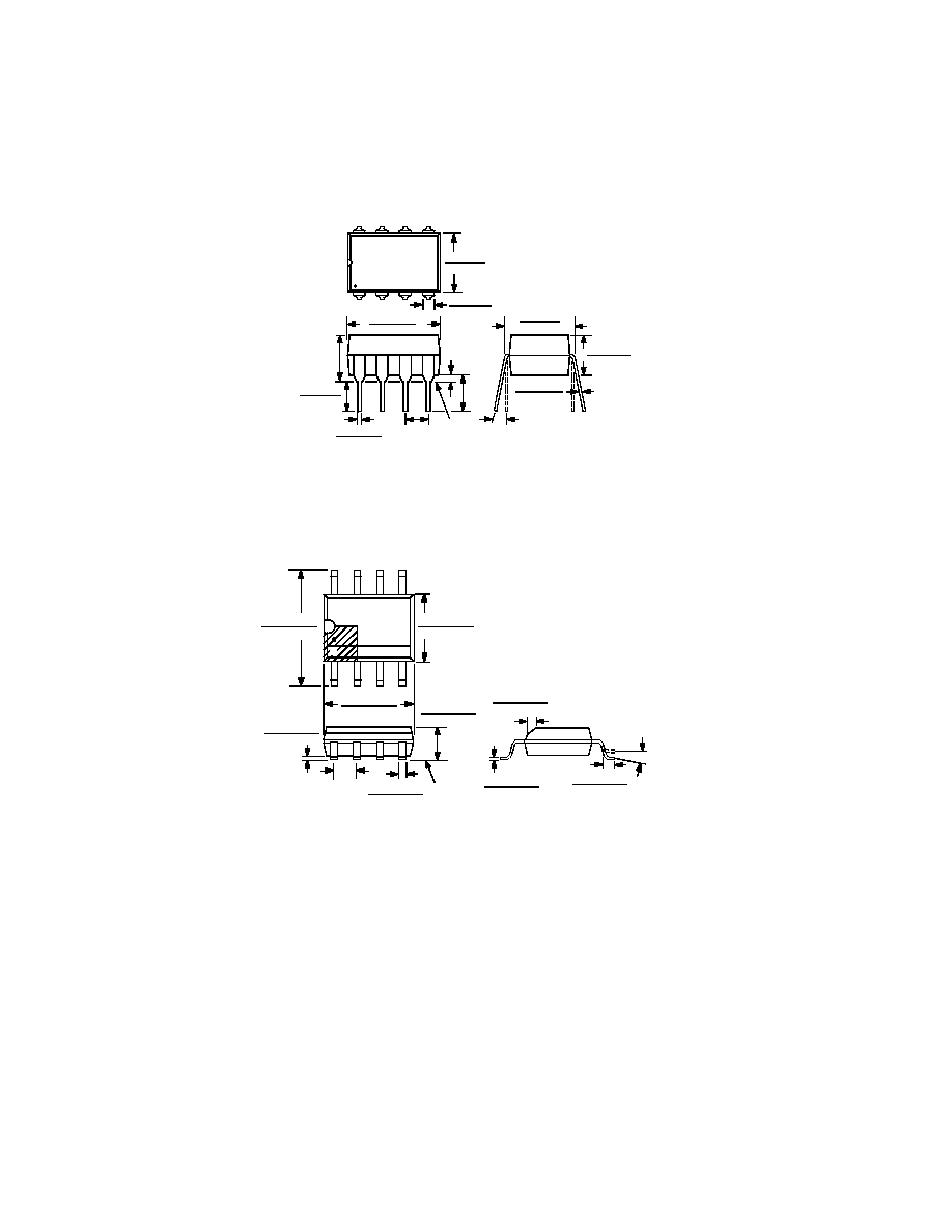
OUTLINE DIMENSIONS
Dimensions shown in inches and (mm).
C1772a1010/97
PRINTED IN U.S.A.
8-Lead Plastic DIP (N-8)
0.160 (4.06)
0.115 (2.93)
0.130
(3.30)
MIN
0.210
(5.33)
MAX
0.015
(0.381) TYP
0.430 (10.92)
0.348 (8.84)
0.280 (7.11)
0.240 (6.10)
4
5
8
1
0.070 (1.77)
0.045 (1.15)
0.022 (0.558)
0.014 (0.356)
0.325 (8.25)
0.300 (7.62)
0°- 15°
0.100
(2.54)
BSC
0.015 (0.381)
0.008 (0.204)
SEATING
PLANE
0.195 (4.95)
0.115 (2.93)
8-Lead Narrow-Body (SO-8)
SEATING
PLANE
4
5
8
1
0.0688 (1.75)
0.0532 (1.35)
0.1574 (4.00)
0.1497 (3.80)
0.2440 (6.20)
0.2284 (5.80)
0.1968 (5.00)
0.1890 (4.80)
0.0192 (0.49)
0.0138 (0.35)
0.0500 (1.27) BSC
0.0098 (0.25)
0.0040 (0.10)
0.0098 (0.25)
0.0075 (0.19)
×
45
°
0.0196 (0.50)
0.0099 (0.25)
0.0500 (1.27)
0.0160 (0.41)
0
°
- 8
°