 | ÐлекÑÑоннÑй компоненÑ: SSM2160S | СкаÑаÑÑ:  PDF PDF  ZIP ZIP |
Äîêóìåíòàöèÿ è îïèñàíèÿ www.docs.chipfind.ru
REV. 0
Information furnished by Analog Devices is believed to be accurate and
reliable. However, no responsibility is assumed by Analog Devices for its
use, nor for any infringements of patents or other rights of third parties
which may result from its use. No license is granted by implication or
otherwise under any patent or patent rights of Analog Devices.
a
SSM2160/SSM2161
One Technology Way, P.O. Box 9106, Norwood, MA 02062-9106, U.S.A.
Tel: 617/329-4700
World Wide Web Site: http://www.analog.com
Fax: 617/326-8703
© Analog Devices, Inc., 1996
6- and 4-Channel, Serial Input
Master/Balance Volume Controls
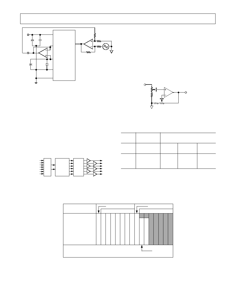
FUNCTIONAL BLOCK DIAGRAM
POWER
SUPPLY AND
REFERENCE
GENERATOR
VCA
CH1 IN
CH1 OUT
CLK
DATA
LD
WRITE
V+
V
V
REF
5-BIT
CHANNEL
DAC
VCA
CH2 IN
CH2 OUT
5-BIT
CHANNEL
DAC
VCA
CH3 IN
CH3 OUT
5-BIT
CHANNEL
DAC
VCA
CH4 IN
CH4 OUT
5-BIT
CHANNEL
DAC
VCA
CH5 IN
CH5 OUT
5-BIT
CHANNEL
DAC
VCA
CH6 IN
CH6 OUT
5-BIT
CHANNEL
DAC
7-BIT
MASTER
DAC
SHIFT REGISTER
AND
ADDRESS
DECODER
STEP SIZE
ADJUST
CH SET
MSTR SET
MSTR OUT
FEATURES
Clickless Digitally Controlled Level Adjustment
SSM2160: Six Channels
SSM2161: Four Channels
7-Bit Master Control Gives 128 Levels of Attenuation
5-Bit Channel Controls Give 32 Levels of Gain
Master/Channel Step Size Set by External Resistors
100 dB Dynamic Range
Automatic Power On Mute
Excellent Audio Characteristics:
0.01% THD+N
0.001% IMD (SMPTE)
90 dBu Noise Floor
80 dB Channel Separation
90 dB SNR
Single and Dual Supply Operation
APPLICATIONS
Home Theater Receivers
Surround Sound Decoders
Circle Surround* and AC-3* Decoders
DSP Soundfield Processors
HDTV and Surround TV Audio Systems
Automotive Surround Sound Systems
Multiple Input Mixer Consoles and Amplifiers
GENERAL DESCRIPTION
The SSM2160 and SSM2161 allow digital control of volume of
six and four audio channels, respectively, with a master level
control and individual channel controls. Low distortion VCAs
(Voltage Controlled Amplifiers) are used in the signal path. By
using controlled rate-of-change drive to the VCAs, the "click-
ing" associated with switched resistive networks is eliminated in
the Master control. Each channel is controlled by a dedicated
5-bit DAC providing 32 levels of gain. A master 7-bit DAC
feeds every control port giving 128 levels of attenuation. Step
sizes are nominally 1 dB and can be changed by external
resistors. Channel balance is maintained over the entire master
control range. Upon power-up, all outputs are automatically
muted. A three- or four-wire serial data bus enables interfacing
with most popular microcontrollers. Windows
* software and an
evaluation board for controlling the SSM2160 are available.
The SSM2160 can be operated from single supplies of +10 V to
+20 V or dual supplies from
±
5 V to
±
10 V. The SSM2161 can
be operated from single supplies of +8.5 V to +20 V (for
automotive applications) or dual supplies from
±
4.25 V to
±
10 V. An on-chip reference provides the correct analog
common voltage for single supply applications. Both models
come in P-DIP and SO packages. See the Ordering Guide for
more details.
*Circle Surround is a registered trademark of Rocktron Corporation.
AC-3 is a registered trademark of Dolby Labs, Inc. Windows is a regis-
tered trademark of Microsoft Corp.
2
REV. 0
SSM2160/SSM2161SPECIFICATIONS
(V
S
= 6 V, T
A
= +25 C, A
V
= 0 dB, f
AUDIO
= 1 kHz, f
CLOCK
=
250 kHz, R
L
= 10 k
, unless otherwise noted)
Parameter
Symbol
Conditions
Min
Typ
Max
Units
AUDIO PERFORMANCE
Noise floor
NFL
V
IN
= GND, BW= 20 kHz, A
V
= 0 dB
1
90
dBu
Total Harmonic Distortion + Noise
THD+N
2nd & 3rd Harmonics Only, V
OUT
= 0 dBu
2
A
V
= 0 dB
0.01
0.035 %
Channel Separation
Any Channel to Another
80
dB
Dynamic Range
NFL to Clip Point
100
dB
ANALOG INPUT
Maximum Level
V
IN
max
V
S
=
±
10 V
1.8
V rms
Impedance
Z
IN
Any Channel
10
k
ANALOG OUTPUT
Maximum Level
3
V
S
=
±
10 V, All Conditions of Master
Attenuation and Channel Gain
1.8
V rms
Impedance
Z
OUT
10
Offset Voltage
20
mV
Minimum Resistive Load
R
L
min
10
k
Maximum Capacitive Load
C
L
max
50
pF
MASTER ATTENUATOR ERROR
Measured from Best Fit of All Channels
from 0 dB and 127 dB (or Noise Floor)
A
V
= 0 dB
Channel Gain = 0 dB
±
0.5
dB
A
V
= 20 dB
Channel Gain = 0 dB
±
1.0
dB
A
V
= 40 dB
Channel Gain = 0 dB
±
2.0
dB
A
V
= 60 dB
Channel Gain = 0 dB
±
2.5
dB
CHANNEL MATCHING
±
1.0
dB
CHANNEL GAIN ERROR
Master Attenuation = 0 dB
A
V
= 0 dB
±
0.5
dB
A
V
= +10 dB
±
1.0
dB
A
V
= +31 dB
±
2.0
dB
MUTE ATTENUATION
V
IN
= 0 dBu
95
dB
VOLTAGE REFERENCE
V
REF
Accuracy
Percent of
(V
+
)
+
(V )
2
±
5
%
Output Impedance
5
CONTROL LOGIC
Logic Thresholds
High (1)
Re: DGND
2.0
V
Low (0)
0.8
V
Input Current
±
1
µ
A
Clock Frequency
1
1000
kHz
Timing Characteristics
See Timing Diagrams
POWER SUPPLIES
Voltage Range
SSM2160
V
S
Single Supply
+10
+20
V
SSM2161
+8.5
+20
V
SSM2160
V+, V
Dual Supply
±
5
±
10
V
SSM2161
±
4.25
±
10
V
Supply Current
No Load
20
28
mA
NOTES
1
Master = 0 dB; Channel = 0 dB.
2
Input level adjusted accordingly. 0 dBu = 0.775 V rms.
3
For other than
±
10 V supplies, maximum is V
S
/4.
Specifications subject to change without notice.
SSM2160/SSM2161
3
REV. 0
Timing Characteristics
Timing
Symbol
Description
Min
Typ
Max
Units
t
CL
Input Clock Pulse Width, Low
200
ns
t
CH
Input Clock Pulse Width, High
200
ns
t
DS
Data Setup Time
50
ns
t
DH
Data Hold Time
75
ns
t
CW
Positive CLK Edge to End of Write
100
ns
t
WC
Write to Clock Setup Time
50
ns
t
LW
End of Load Pulse to Next Write
50
ns
t
WL
End of Write to Start of Load
50
ns
t
L
Load Pulse Width
250
ns
t
W3
Load Pulse Width (3-Wire Mode)
250
ns
NOTES
1. An idle HI (CLK-HI) or idle LO (CLK-LO) clock may be used. Data is latched on the negative edge.
2. For SPI or microwire three-wire bus operation, tie LD to WRITE, and use WRITE pulse to drive both pins. (This generates an automatic internal load signal.)
3. If an idle HI clock is used, t
CW
and t
WL
are measured from the final negative transition to the idle state.
4. The first data byte selects an address (MSB HI), and subsequent MSB LO states set gain/attenuation levels. Refer to the Address/Data Decoding Truth Table.
5. Data must be sent MSB first.
D7
D6
D5
D4
D3
D2
D1
D0
0
0
0
0
1
1
1
1
CLK
DATA
WRITE
LD
t
WL
t
L
t
LW
t
DH
t
DS
t
CH
0
0
1
1
0
1
1
0
CLK
DATA
WRITE
LD
t
CL
D7
t
WC
t
CW
MSB
Figure 1. Timing Diagrams
SSM2160/SSM2161
4
REV. 0
ABSOLUTE MAXIMUM RATINGS
1
Supply Voltage
Dual Supply . . . . . . . . . . . . . . . . . . . . . . . . . . . . . . . . . .
±
18 V
Single . . . . . . . . . . . . . . . . . . . . . . . . . . . . . . . . . . . . . . . +36 V
Logic Input Voltage . . . . . . . . . . . . . . . . . . . . . 0.3 V to +5 V
Operating Temperature Range . . . . . . . . . . . . . 0
°
C to +70
°
C
Storage Temperature Range . . . . . . . . . . . . 65
°
C to +150
°
C
Junction Temperature Range . . . . . . . . . . . . 65
°
C to +165
°
C
Lead Temperature Range (Soldering, 60 sec) . . . . . . . +300
°
C
ESD Ratings
883 (Human Body) Model . . . . . . . . . . . . . . . . . . . . . . 2.5 kV
PACKAGE THERMAL INFORMATION
Package Type
3
JA
JC
Units
24-Pin Plastic P-DIP
60
30
°
C/W
24-Pin SOIC
71
23
°
C/W
20-Pin Plastic P-DIP
65
26
°
C/W
20-Pin SOIC
84
24
°
C/W
NOTES
1
Absolute maximum ratings apply at +25
°
C unless otherwise noted.
2
V
S
is the total supply span from V+ to V.
3
JA
is specified for the worst case conditions, i.e., for device in socket for P-DIP,
packages and for device soldered onto a circuit board for SOIC packages.
ORDERING GUIDE
Temperature
Package
Package
Model
Range
Description
Option
SSM2160P
0
°
C to +70
°
C
24-Lead Plastic DIP N-24
SSM2160S
0
°
C to +70
°
C
24-Lead SOL
R-24
SSM2160S-REEL
0
°
C to +70
°
C
24-Lead SOL
R-24
SSM2161P
0
°
C to +70
°
C
20-Lead Plastic DIP N-20
SSM2161S
0
°
C to +70
°
C
20-Lead SOL
R-20
SSM2161S-REEL
0
°
C to +70
°
C
20-Lead SOL
R-20
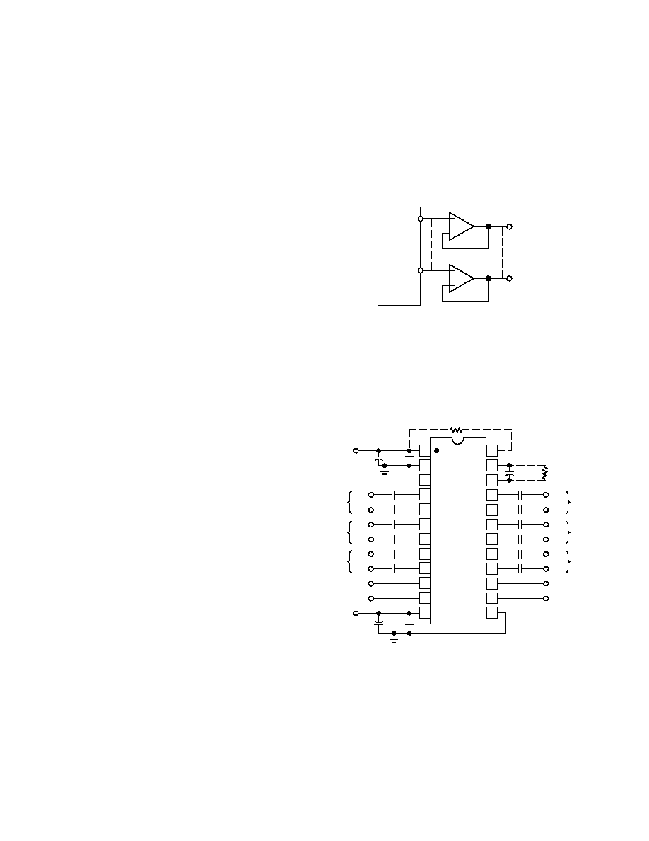
PIN CONFIGURATIONS
24-Lead Epoxy DIP and SOIC
13
16
15
14
24
23
22
21
20
19
18
17
TOP VIEW
(Not to Scale)
12
11
10
9
8
1
2
3
4
7
6
5
SSM2160
V+
VOUT2
MSTR SET
MSTR OUT
CH SET
AGND
V
REF
VOUT1
VIN4
VOUT4
VIN2
VIN1
VOUT3
VIN3
VOUT5
VIN5
WRITE
DATA
VIN6
VOUT6
LD
V
CLK
DGND
20-Lead Epoxy DIP and SOIC
14
13
12
11
17
16
15
20
19
18
10
9
8
1
2
3
4
7
6
5
TOP VIEW
(Not to Scale)
SSM2161
V+
VOUT2
MSTR SET
MSTR OUT
CH SET
AGND
V
REF
VOUT1
VIN4
VOUT4
VIN2
VIN1
VOUT3
VIN3
WRITE
LD
V
DGND
CLK
DATA
SSM2160/SSM2161
5
REV. 0
PIN DESCRIPTIONS
S
SM2160 SSM2161
Pin No.
Pin No.
Name
Function
1
1
V+
V+ is the positive power supply pin. Refer to the Power Supply Connections section for more
information.
2
2
AGND
AGND is the internal ground reference for the audio circuitry. When operating the SSM2160
from dual supplies, AGND should be connected to ground. When operating from a single
supply, AGND should be connected to V
REF
, the internally generated voltage reference. AGND
may also be connected to an external reference. Refer to the Power Supply Connections section
for more details.
3
3
V
REF
V
REF
is the internally generated ground reference for the audio circuitry obtained from a buffered
divider between V+ and V. In a dual-supply application with the AGND pin connected to
ground, V
REF
should be left floating. In a single supply application, V
REF
should be connected to
AGND. Refer to the Power Supply Connections section for more details.
4
4
CH1 OUT
Audio Output from Channel 1.
5
5
CH1 IN
Audio Input to Channel 1.
6
6
CH3 OUT
Audio Output from Channel 3.
7
7
CH3 IN
Audio Input to Channel 3.
8
CH5 OUT
Audio Output from Channel 5.
9
CH5 IN
Audio Input to Channel 5.
10
8
WRITE
A logic LOW voltage enables the SSM2160 to receive information at the DATA input (Pin 15).
A logic HIGH applied to WRITE retains data at their previous settings. See Timing Diagrams.
Serves as CHIP SELECT.
11
9
LD
Loads the information retained by WRITE into the SSM2160 at logic LOW. See Timing
Diagrams.
12
10
V
V is the negative power supply pin. Connect to ground if using in a single supply application.
Refer to the Power Supply Connections section for more details.
13
11
DGND
DGND is the digital ground reference for the SSM2160. This pin should always be connected to
ground. All digital inputs, including WRITE, LD, CLK, and DATA are TTL input compatible;
drive currents are returned to DGND.
14
12
CLK
CLK is the clock input. It is positive edge triggered. See Timing Diagrams.
15
13
DATA
Channel and Master control information flows MSB first into the DATA pin. Refer to Address/
Data Decoding Truth Table, Figure 19, for information on how to control the VCAs.
16
CH6 IN
Audio Input to Channel 6.
17
CH6 OUT
Audio Output from Channel 6.
18
14
CH4 IN
Audio Input to Channel 4.
19
15
CH4 OUT
Audio Output from Channel 4.
20
16
CH2 IN
Audio Input to Channel 2.
21
17
CH2 OUT
Audio Output from Channel 2.
22
18
MSTR SET
MSTR SET is connected to the inverting input of an I-V converting op amp used to generate a
Master Control voltage from the Master Control DAC current output. A resistor connected
from MSTR OUT to MSTR SET reduces the step size of the Master control. See the Adjusting
Step Sizes section for more details. A 10
µ
F capacitor should be connected from MSTR OUT to
MSTR SET to eliminate the zipper noise in the Master control.
23
19
MSTR OUT
MSTR OUT is connected to the output of the I-V converting op amp. See MSTR SET
description.
24
20
CH SET
The step size of the Channel Control can be increased by connecting a resistor from CH SET to
V+. No connection to CH SET is required if the default value of 1 dB per step is desired. Mini-
mum of 10
external resistor. See the Adjusting Step Sizes section for more details.
SSM2160/SSM2161
6
REV. 0
Typical Performance Characteristics
GAIN dB
70
20
60
40
20
0
10
10
1.0
0.1
0.01
0.001
THD+N %
T
A
= +25
°
C
V
S
=
±
6V
V
IN
= 0dBu
R
L
= 10k
C
L
= 50pF
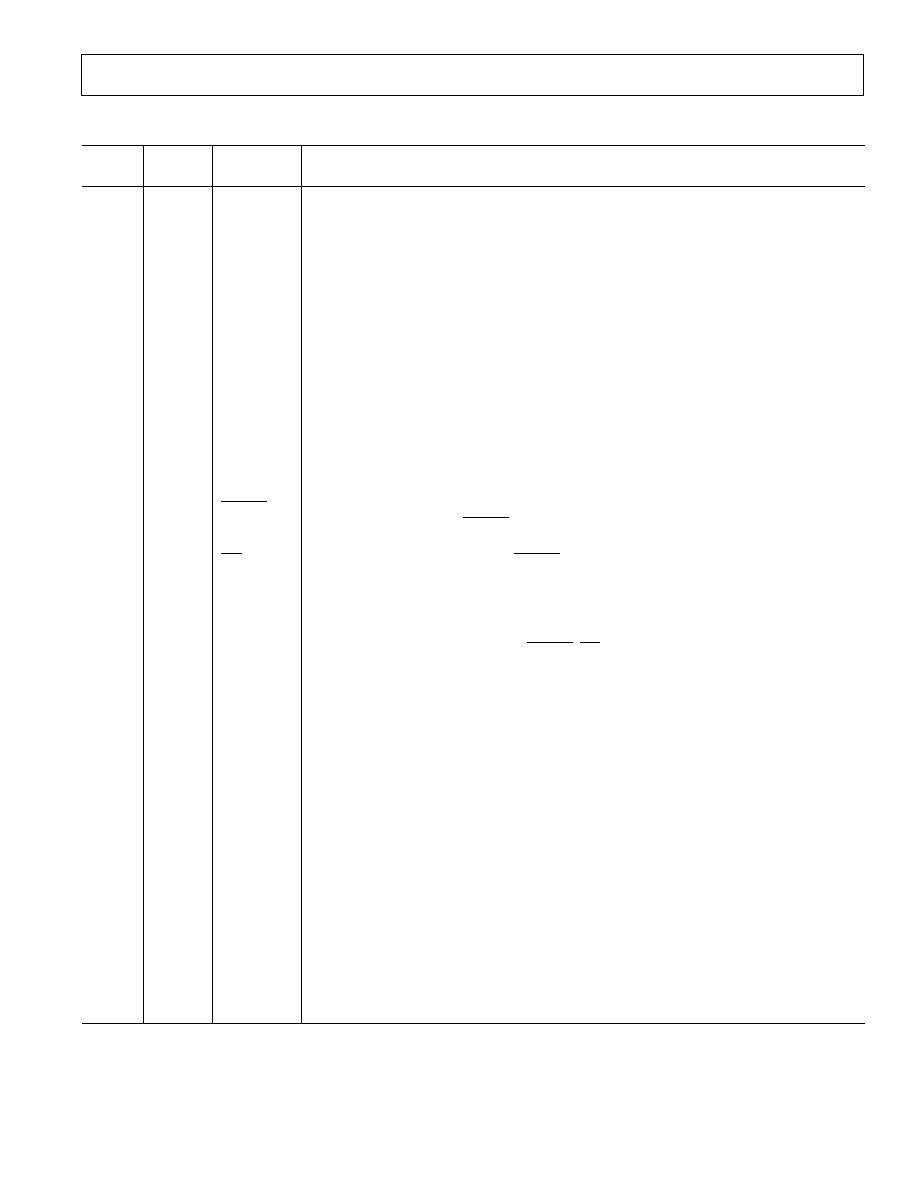
Figure 2. THD vs. Gain
FREQUENCY Hz
0.01
20
30k
100
1k
10k
T
A
= +25
°
C
DUAL SUPPLY OPERATION
V
IN
= 300mVrms@1kHz
R
L
= 10k
, C
L
= 50pF
MASTER/CHANNEL = 0dB
LPF: < 22kHz
V
S
=
±
12V
0.1
THD+N %
0.001
V
S
=
±
6V
Figure 5. THD+N % vs. Frequency
INPUT VOLTAGE Vrms
0.001
0.01
10
0.1
1
0.1
THD+N %
0.01
1.0
T
A
= +25
°
C
SINGLE SUPPLY OPERATION
V
IN
= SINEWAVE @ 1kHz
R
L
= 10k
, C
L
= 50pF
MASTER/CHANNEL = 0dB
V
S
= 15V
V
S
= 20V
V
S
= 10V
Figure 3. THD+N % vs. Amplitude
FREQUENCY Hz
40
80
20
20k
100
1k
10k
CHANNEL SEPARATION dB
50
60
70
120
90
100
110
T
A
= +25
°
C
V
S
=
±
6V
V
IN
= 1Vrms @ 1kHz
V
IN
= GND (NON SELECTED CH)
R
L
= 100k
, C
L
= 50pF
LPF: < 22kHz
Figure 6. Channel Separation vs.
Frequency
GAIN dB
NOISE dBu
60
95
110
70 60
40
40 30 20 10
0
10
20
31
65
90
100
105
80
85
70
75
T
A
= 25
°
C
V
S
=
±
6V
V
IN
= GND
Figure 8. Noise vs. Gain
INPUT VOLTAGE Vrms
0.5
0.1
0.005
0.05
10
0.1
1
THD+N %
0.01
T
A
= +25
°
C
DUAL SUPPLY OPERATION
V
IN
= SINEWAVE @ 1kHz
R
L
= 10k
, C
L
= 50pF
MASTER/CHANNEL = 0dB
V
S
=
±
12V
V
S
=
±
5V
V
S
=
±
6V
Figure 4. THD+N % vs. Amplitude
FREQUENCY Hz
40
80
50
60
70
120
90
100
110
20
30k
100
OUTPUT dB
1k
10k
T
A
= +25
°
C
V
S
=
±
6V
V
IN
= 1Vrms @ 1kHz
R
L
= 10k
, C
L
= 50pF
Figure 7. Mute vs. Frequency
SSM2160/SSM2161
7
REV. 0
FREQUENCY kHz
0
22
2
4
6
8
10 12
14 16 18 20
0
70
140
10
60
80
90
30
50
20
40
120
110
100
130
AMPLITUDE dBu
T
A
= 25
°
C
V
S
=
±
12V
VIN
= 0dBu @ 1kHz
R
L
= 100k
MASTER = 20dB
CHANNEL = 0dB
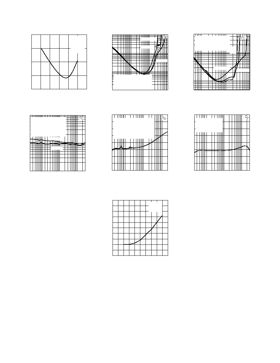
Figure 9a. THS vs. Frequency (FFT)
INPUT AMPLITUDE Vrms
0.1
0.010
0.05
5
0.1
1
0.001
T
A
= +25
°
C
V
S
=
±
12V
SMPTE 4:1
IM-FREQ 60Hz/7kHz
R
L
= 100k
0.0001
1MD (SMPTE) %
Figure 10. SMPTE IM vs. Amplitude
V rms
FREQUENCY kHz
0
22
2
4
6
8
10 12 14 16 18 20
0
70
140
10
60
80
90
30
50
20
40
120
110
100
130
T
A
= 25
°
C
V
S
=
±
12V
VIN = 31dBu @ 1Hz
R
L
= 100K
MASTER = 0dB
CHANNEL = 0dB
AMPLITUDE dBu
9b. THD vs. Frequency (FFT)
FREQUENCY kHz
0
22
2
4
6
8
10 12 14 16 18 20
0
70
140
10
60
80
90
30
50
20
40
120
110
100
130
AMPLITUDE dBu
T
A
= 25
°
C
V
S
=
±
12V
R
L
= 100k
A MASTER = 0dB
CHANNEL = +31dB
B MASTER/CHANNEL = 0dB
B
A
Figure 11. Noise Floor FFT
SUPPLY VOLTAGE Volts
±
4
±
13
±
6
±
7
±
8
±
9
±
10
±
11
±
12
±
5
25
22
15
SUPPLY CURRENT mA
21
20
19
23
24
18
17
16
Figure 13. I
SY
vs. V
S
FREQUENCY kHz
0
22
2
4
6
8
10 12 14 16 18
20
0
70
140
10
60
80
90
30
50
20
40
120
110
100
130
AMPLITUDE dBu
T
A
= 25
°
C
V
S
=
±
12V
VIN = 31dBu @ 1kHz
R
L
= 100k
MASTER = 0dB
CHANNEL = 31dB
Figure 9c. THD vs. Frequency (FFT)
FREQUENCY Hz
20
60
20
30k
100
PSR dB
1k
10k
30
40
50
100
70
80
90
PSR
PSR+
T
A
= +25
°
C
V
S
=
±
6V
±
10%
LPF = <22kHz
MASTER = 0dB
CHANNEL = 0dB
Figure 12. PSR vs. Frequency
SSM2160/SSM2161
8
REV. 0
APPLICATIONS INFORMATION
General
The SSM2160 and SSM2161 are six and four channel volume
controls intended for multichannel audio applications. While
dual channel controls sufficed for "stereo" applications, the
rapidly emerging home theater "surround sound" and auto
sound venues demand both six and four channel high perfor-
mance controls. The following information applies equally to
the SSM2160 and SSM2161, except where noted. Line level
signals are fed to the six high impedance inputs. The system
microcontroller sets the gain of the six channels via a three or
four wire data bus. In a home theater receiver, the outputs may
be fed to the power amplifiers or buffered and connected to pre-
out/amp-in ports on the rear panel. Refer to Figure 17 for a
typical signal chain using the SSM2160. The Master control
serves the "Volume" control function, and the channel control
serves the "Balance" function. The six channel capability allows
complete control of the front left, front right, center, rear left,
rear right, and sub-bass audio channels.
Power Supplies vs. Signal Levels
The SSM2160 can be operated from dual supplies from
±
5 V to
±
10 V and from single supplies from +10 V to +20 V. The
SSM2161 can be operated from dual supplies from
±
4.25 V to
±
10 V for automotive applications and from single supplies from
+8.5 V to +20 V. In order to keep power dissipation to a
minimum, use the minimum power supply voltages that will
support the maximum input and output signal levels. The peak-
to-peak output signal level must not exceed 1/4 of the total
power supply span, from V+ to V. This restriction applies for all
conditions of input signal levels and gain/attenuation settings.
Table I shows supply voltages for several typical output signal
levels for both devices. An on-chip buffered voltage divider
provides the correct analog common voltage for single supply
applications.
Table I. Signal Levels vs. Power Supplies
SSM2160
Max Output,
Max Output,
V rms (V p-p)
dBu
Single +V
S
Dual
V
S
0.9 (2.5)
+1.3
10 V
±
5 V
1.1 (3.0)
+3.0
12 V
±
6 V
1.3 (3.7)
+4.5
15 V
±
7.5 V
1.8 (5.0)
+7.3
20 V
±
10 V
SSM2161
Max Output,
Max Output,
V rms (V p-p)
dBu
Single +V
S
Dual V
S
0.75 (2.1)
+1.0
8.5 V
±
4.25 V
1.1 (3.0)
+3.0
12 V
±
6 V
1.3 (3.7)
+4.5
15 V
±
7.5 V
1.8 (5.0)
+7.3
20 V
±
10 V
Dual Power Supplies
As shown in Figure 14, the AGND pin should be connected to
ground and V
REF
should be left floating. The digital ground pin,
DGND, should always be connected to ground for either single-
or dual-supply configurations. Pins 1 and 12 should each have
a 10
µ
F capacitor connected to ground, with a 0.1
µ
F capacitor
placed as close as possible to the SSM2160 device to help
reduce the effects of high frequency power supply noise. When
a switching power supply is used, or if the power supply lines
are noisy, additional filtering of the power supply lines may be
required.
+
1
2
V+
0.1µF
10µF
V
10µF
12
13
DGND
V
V
REF
AGND
V+
SSM2160
+
0.1µF
Figure 14. Dual Supply Configuration
Single Power Supply
When a single supply is used, it is necessary to connect AGND
(Pin 2) to V
REF
(Pin 3) as shown in Figure 15. V
REF
supplies a
voltage midway between the V+ and V pins from a buffered
resistive divider. When supplying this reference to stages ahead
of the SSM2160 (to eliminate the need for input dc blocking
capacitors, for example), the use of an additional external
buffer, as shown in Figure 16 may be necessary to eliminate any
noise pickup.
+
+
V+
0.1µF
10µF
0.1µF
10µF
3
1
2
12
13
DGND
V
V
REF
AGND
V+
SSM2160
Figure 15. Single Supply Configuration
SSM2160/SSM2161
9
REV. 0
+
+
V+
0.1µF
10µF
0.1µF
10µF
3
1
2
12
13
DGND
V
V
REF
AGND
V+
SSM2160
CHnIN
REF
OUT
Figure 16. Single Supply Operation with V
REF
Buffer
Signal Chain Considerations
The SSM2160 is capable of providing an extremely wide control
range, from 127 dB of attenuation (limited only by the noise
floor) to +31 dB of gain. When configuring the system, the
SSM2160 should be in the signal chain where input signals allow
the minimum VCA gain to be used, thus ensuring the lowest
distortion operation. In consumer products, sources that
supply line level signals include FM/AM Tuner, Phono Preamp,
Cassette Deck, CD, Laserdisc, VCR, LINE, AUX and Micro-
phone Preamp. Figure 17 shows a typical application where the
SSM2160 has been placed between a surround-sound decoder
and the power amplification stages. This allows the user to
adjust both volume and balance between six speakers through the
use of the Master and Channel controls.
FM/AM TUNER
PHONO PREAMP
CASSETTE DECK
COMPACT DISK
LASER DISK
VCR
MICROPHONE
MUX
SURROUND
SOUND
DECODER
SSM2160
TO
SPEAKERS
POWER AMPS
VOLUME AND
BALANCE
CONTROLS
LINE LEVEL INPUTS STEREO PAIRS
Figure 17. Typical Signal Chain Using the SSM2160
Digital Control Range Plan
The SSM2160 may be modelled as six ganged potentiometers
followed by individual programmable gain channel amplifiers, as
shown in Figure 18. In actuality, each channel's signal level is
set by a VCA that can give gain or attenuation, depending upon
the control voltage supplied. The input potentiometers have a
maximum gain 0 dB (unity), a minimum gain of 127 dB, and
change in 1 dB steps. The channel amplifiers each have mini-
mum gain of 0 dB and a maximum gain of +31 dB and also
change in 1 dB steps. The data settings for the attenuation of
the master "potentiometer" and the channel "amplifier" are
shown in Table II.
OUTPUT
CHANNEL
INPUT
0dB
127dB
31dB
0dB
MASTER
Figure 18. Potentiometer Representation of SSM2160
(One Channel Only)
Table II. Master and Channel Control
Data
dB
Hex
Binary
Master
Min Atten
0
7F
1111111
Max Atten
127
00
0000000
Channel
Max Gain
+31
00
00000
Midgain
+15
10
10000
Min Gain
0
1F
11111
When using Channel controls as balance controls, the center
would be with Channel = 10
h
(or 0F
h
if desired). Increasing the
gain to the maximum would occur at Channel = 00
h
. Reducing
the gain to minimum would occur at Channel = 1F
h
.
SELECTION
ADDRESS MODE
ADDRESS
DATA MODE
DATA
7-BIT MASTER DAC
5-BIT CHANNEL DAC 1
5-BIT CHANNEL DAC 2
5-BIT CHANNEL DAC 3
5-BIT CHANNEL DAC 4
5-BIT CHANNEL DAC 5
5-BIT CHANNEL DAC 6
NO DAC SELECTED
1
1
1
1
1
1
1
1
X
X
X
X
X
X
X
X
X
X
X
X
X
X
X
X
X
X
X
X
X
X
X
X
X
X
X
X
X
X
X
X
0
0
0
0
1
1
1
1
0
0
1
1
0
0
1
1
0
1
0
1
0
1
0
1
0
0
0
0
0
0
0
0
1
1
1
1
1
1
1
X
X
X
X
X
X
X
X = "DON'T CARE"
SHADED AREA IS DATA
0 = MUTE,
1 = UN-MUTE
MSB
MSB
LSB
LSB
X
X
X
X
X
Figure 19. Interface Characteristics, DAC Address/Data Decoding Truth Table
SSM2160/SSM2161
10
REV. 0
Serial Data Input Format
The standard format for data sent to SSM2160 is an address
byte followed by a data byte. This is depicted in the truth table,
Figure 19. Two 8-bit bytes are required for each Master and
each of the six channel updates. The first byte sent contains the
address and is identified by the MSB being logic high. The
second byte contains the data and is identified by the MSB being
logic low. The 7 LSBs of the first data byte set the attenuation level
from 0 dB to 127 dB for the Master. The 5 LSBs of the byte set
the Channel gain levels from 0 dB to 31 dB.
Serial Data Control Inputs
The SSM2160 provides a simple 3- or 4-wire serial interface--
see the timing diagram in Figure 1. Data is presented to the
DATA pin and the serial clock to the CLK pin. Data may be
shifted in at rates up to 1 MHz (typically).
The shift register, CLK, is enabled when the WRITE input is
low. The WRITE thus serves as a Chip Select input; however,
the shift register contents are not transferred to the holding
register until the rising edge of LD. In most cases, WRITE and
LD
will be tied together, forming a tradition 3-wire serial interface.
To enable a data transfer, the WRITE and LD inputs are driven
logic low. The 8-bit serial data, formatted MSB first, is input on
the DATA pin and clocked into the shift register on the falling
edge of CLK. The data is latched on the rising edge of WRITE
and LD.
Table III. Input/Output Levels vs. Attenuation/Gain
Input
Gain/Loss
Output
dBu
mV rms
Master
Channel
Net dBu
mV rms
0
775
31
31
0
0
775
31
22
0
31
31
0
775
28
31
0
31
31
3
1100
Saturation Prevention
Unlike a passive potentiometer, the SSM2160 can give up to
+31 dB of gain, thereby creating a potential for saturating the
VCAs, resulting in an undesirable clipping or overload condi-
tion. Careful choice of input signal levels and digital gain
parameters will eliminate the possibility. A few of the many
acceptable gain and attenuation settings that keep the signals
within the prescribed limits are shown in Table III. The
input and output levels are given in mV rms and dBu (0 dBu
= 0.775 V rms).
Line one of the table: the master is not allowed to have less than
31 dB attenuation, and the channel is allowed +31 dB of gain.
Since the net gain is zero, there is no possibility of overload with
the expected maximum input signal.
Line two of the table shows that input signal limited to 31 dBu
will allow +31 dB of Channel gain and 0 dB of Master attenua-
tion. With an input below 31 dBu, the output will never
exceed 0 dBu, so no overloading is possible.
Line Three of the table allows an input of 28 dBu, Master
attenuation of 0 dB, and 31 dB Channel gain. The output is a
maximum of 3 dBu (1.1 V rms), which is acceptable for power
supplies of
±
6 V or more. So long as V p-p < V
SUPPLY
/4, there
will be no overloading (See Table I).
If unity overall gain is required from the SSM2160, there should
be no net gain between the master (loss) and channel (gain),
with both at their lowest attenuation position. Minimum
channel gain is recommended for minimum distortion.
MASTER
DAC
CHANNEL
DAC
IN
OUT
R
C
I
FS
SET
SUMMATION
RESISTOR
"R"
i
SIGNAL
V+
R
M
C
R
M
, R
C
, C
EXTERNAL
SSM2160
Figure 20. VCA Control Scheme
Control Range and Channel Tracking
Each Channel VCA is controlled by its own DAC's output, plus
the control signal from the master DAC. This is shown in
Figure 21. Channel DACs are configured to increase the gain of
the VCA in 1 dB steps from zero to 31 dB. Thus, the midpoint
(15, or 16 if you prefer) should be chosen as the center setting
of the electronic balance controls. Since the master DAC feeds
all summation nodes, the attenuation of all VCAs simulta-
neously change from 0 dB to the noise floor.
Maximum Attenuation of all channels occurs when the Master is
set to 127 dB attenuation, and the Channel is set to 0 dB gain.
Minimum Attenuation of all channels occurs when the Master is
set at 0 dB, and the Channel is set to +31 dB.
Once the channel to channel balance has been set, the Master
may be changed without changing the balance. This is shown
graphically in Figure 21.
+31
+16
0
16
32
48
64
80
96
112
128
0 0 0 0 0
1 1 1 1 1
0 0 0 0 0
1 1 1 1 1
CHANNEL
GAIN
CHANNEL
GAIN
CHANNEL
GAIN
MASTER
ATTENUATION
+31
+16
0
+31
+16
0
NOISE FLOOR
0 0 0 0 0 0
NET GAIN/ATTEN
1 1 1 1 1 1
Figure 21. Practical Control Range
Master/Channel Step Sizes
The details of the DAC control of the Channel VCAs is
depicted in Figure 20. A 7-bit current output DAC and an op
amp converts the digitally commanded master control level to
an analog voltage. A capacitor across the feedback resistor
limits the rate of change at the output to prevent clicking. A
5-bit DAC converts the digitally commanded channel control
level to a voltage via a resistor R. These two control signals sum
in resistor R and are fed to the channel VCA. Although we
SSM2160/SSM2161
11
REV. 0
present the attenuation and gain as two separate items, in fact,
the VCA can be operated smoothly from a gain condition to an
attenuation. The master and channel step sizes default to 1 dB
in the absence of external components. The step sizes can be
changed by the addition of external resistors if finer resolution is
desired.
Control Range vs. Step Size
Before adjusting step sizes from the standard 1 dB, consider the
effect on control range. The master control and the channel
control provide 1 dB step sizes, which may be modified by the
addition of external resistors. As the total number of steps is
unchanged, reduction of the step size results in less control
range. The range of the control is:
Range = Step Size (dB)
×
(Number of Levels Used)
Since the master volume control operates from a 7-bit word, its
DAC has 128 levels (including 0). The channel volume control
DAC is a 5-bit input, so there are 32 levels for volume control
(including 0). As can be seen in Figure 21, the practical control
range is set by the noise floor. It can be advantageous to reduce
the master step size to give finer steps from zero attenuation
down to the noise floor.
Reducing Master Step Size
To reduce the master step size, place a resistor, R
M,
between
MSTR SET and MSTR OUT. The master step size of the
master volume control will then become:
R
M
=
1700 X
MASTER
1 X
MASTER
where, X
MASTER
is the desired master control step size in
decibels. See Figure 22 for practical values of R
M
. Note that
the step size for the master control can only be adjusted to less
than 1 dB. No resistor is required for the default value of 1 dB
per step. For larger step sizes, use digital control. Noninteger
dB step sizes can be obtained by using digital control and a
reduced step size.
R
MASTER
1.0
0.8
0
10
2
10
5
10
3
MASTER STEP SIZE dB
10
4
0.6
0.4
0.2
Figure 22. Master Step Size vs. R
M
Example: Modifying Master Step Size to 0.5 dB
A master step size of 0.5 dB is desired for the master control,
while a 1 dB step size is adequate for the channel control. Using
the above equation or Figure 22, R
M
is found to be 1700
and
is connected between MSTR SET and MSTR OUT. There
could be some variation from lot to lot, so applications requiring
precise step size should include a fixed plus a trimmer to span
the calculated value
±
25%. In this example, R
C
is not needed
as the default channel step size is already 1 dB. CH SET is left
floating. With this step size, the dynamic range of the master
control is:
DNR = 0.5
×
127 dB = 63.5 dB
In this configuration, the maximum master volume is 0 dB,
while the minimum volume is 63.5 dB. Since the channel
volume can still provide 0 dB to 31 dB of gain, the total system
gain can vary between 63.5 dB and 32 dB. Note that a 0 dB
command setting to the master control always results in unity
gain, regardless of the step size.
Channel Step Size
The channel DACs' full-scale current is set by an internal
resistor to the V+. By shunting this resistor, the full-scale
current, and therefore the step size, will increase. No provisions
are available for reducing the channel step size. To increase the
channel step size, place a resistor, R
C
, from CH SET to V+.
Note that a 0 dB setting for a channel will always give unity
gain, regardless of how large or small the step size is. This is
true for both the master and channel volume controls.
R
CHAN
1.5
1.4
1.0
10
1
10
3
10
2
CHANNEL STEP SIZE
1.3
1.2
1.1
Figure 23. Channel Step Size vs. R
C
Example: Modifying Channel Step Size
A channel step size of 1.3 dB is desired. From Figure 23 we see
that a 40
resistor (approximately) connected from CH SET to
V+ is required. As this varies from lot to lot, the exact value
should be determined empirically, or a fixed resistor plus
trimmer potentiometer should be used. Take care not to short
Pin 24 to Pin 1 as damage will result.
Muting
The SSM2160 offers master and channel muting. On power
up, the master mute is activated, thus preventing any transients
from entering the signal path and possibly overloading amplifi-
ers down the signal path. Mute is typically better than 95 dB
relative to a 0 dBu input. Due to design limitations, the individual
channel muting results in increased signal distortion in the
unmuted channels. Users should determine if this condition is
acceptable in the particular application.
SSM2160/SSM2161
12
REV. 0
DC Blocking and Frequency Response
All internal signal handling uses direct coupled circuitry.
Although the input and output dc offsets are small, dc blocking
is required when the signal ground references are different.
This will be the case if the source is from an op amp that uses
dual power supplies (i.e.,
±
6 V), and the SSM2160 uses a single
supply. If the signal source has the capability of operating with
an externally supplied signal, connect the V
REF
(Pin 3) to the
source's external ground input either directly or through a
buffer as shown in Figure 16.
The same consideration is applied to the load. If the load is
returned to AGND, no capacitor is required. When the
SSM2160 is operated from a single supply, there will be a dc
output level of +V
S
/2 at the output. This will require dc blocking
capacitors if driving a load referred to GND.
When dc blocking capacitors are used at the inputs and outputs,
they form a high pass filter with the input and load resistance
both of which are typically 10 k
. To calculate the lower 3 dB
frequency of the high-pass filter formed by the coupling capacitor
and the input resistance, use the following formulas:
f
C
= 1/(2
RC), or
C = 1/(2
R f
C
)
where R is the typically 10 k
input resistance of the SSM2160
or the load resistance. C is the value of the blocking capacitor
when f
C
is known.
If a cutoff frequency of 20 Hz were desired, solving for C gives
0.8
µ
F for the input or output capacitor. A higher load imped-
ance will allow smaller output capacitors to give the same 20 Hz
cutoff. Note that the overall low-pass filter will be the cascade
of the two, so the response will be 6 dB at 20 Hz. A practical
and economical choice would be 1
µ
F/15 V electrolytics.
Signal/Noise Considerations and Channel "Center" Gain
The SSM2160 should be placed in the signal flow where levels
are high enough to result in low distortion and good SNR, but
not so high to require unusually high power supplies. In a
typical application, input and output signal levels will be in the
300 mV
±
200 mV rms range. This level is typically available
from internal and external sources. As previously mentioned,
the +31 dB of gain available in the VCA is usually used for
balancing the various channels and is usually set to +15 dB or
+16 dB in its "center" position. Due to the nature of VCAs'
performance vs. gain, the minimum gain that will allow balanc-
ing the channels should be used. If no balance function is
required, the channel gain should be set to 0 dB. Use the
lowest value of "centered" gain when less than the full balance
range is needed. For example, if only
±
6 dB channel gain
variations were needed, the "center" could be set at +6 dB,
giving +6 dB
±
6 dB, rather than at +15 dB
±
6 dB. This
would result in improved S/N ratio and less distortion.
Digital Interface
Digital logic signals have fast rising and falling edges that can
easily be coupled into the signal and ground paths if care is not
taken with PC board trace routing, ground management, and
proper bypassing. In addition, limiting the high state logic
signal levels to 3.5 V will minimize noise coupling.
Load Considerations
The output of each SSM2160 channel must be loaded with a
minimum of 10 k
. Connecting a load of less than 10 k
will
result in increased distortion and may cause excessive internal
heating with possible damage to the device. Capacitive loading
should be kept to less than 50 pF. Excessive capacitive loading
may increase the distortion level and may cause instability in the
output amplifiers. If your application requires driving a lower
impedance or more capacitive load, use a buffer as shown in
Figure 24.
VOUT 1
VOUT 6
SSM2160
CH1 OUT
CH6 OUT
1/2 SSM2135
1/2 SSM2135
Figure 24. Output Buffers to Drive Capacitive Loads
Windows Software
Windows software is available to customers from Analog
Devices to interface the serial port of a PC (running Windows
3.1) with the SSM2160. Contact your sales representative for
details on obtaining the software. For more details, see the
Evaluation Board section.
13
16
15
14
24
23
22
21
20
19
18
17
12
11
10
9
8
1
2
3
4
7
6
5
SSM2160
+
0.1µF
10µF
+
0.1µF
10µF
+
10µF
R
M
*
OUT
IN
CH 2
OUT
IN
CH 4
OUT
IN
CH 6
DATA
CLK
OUT
IN
CH 1
OUT
IN
CH 3
OUT
IN
CH 5
V
WRITE
LD
V+
*
*OPTIONAL SEE "STEP SIZE"
**TYPICAL 110µF: SEE "D.C. BLOCKING"
R
C
*
**
Figure 25. Typical Application Circuit (Dual Supply)
SSM2160/SSM2161
13
REV. 0
Controlling Stereo Headphones Level and Balance
Figure 26 shows how the SSM2160 can be configured to drive a
stereo headphone output amplifier. Note that the minimum
load specification precludes driving headphones directly. This
example assumes that audio left and right signals are being fed
into Channels 1 and 2, respectively. Additional amplifiers could
be connected to the outputs to provide additional channels.
The master control will set the loudness, and the channel
controls will set the balance. The headphone amplifiers may be
connected to the same power supplies as the SSM2160. The
stereo audio signals are directly coupled to the noninverting
input of both op amps. Depending upon the headphones and
the signal levels, the optional R1 may be selected to provide
additional gain. The gain is determined by:
A
V
=
1
+
R2
R1
As an example, suppose a high impedance headphone (600
)
required a minimum of 25 mW to produce the desired loudness.
Further, suppose the system design made available an output
level from the SSM2160 of 300 mV. If the output were buffered
without gain and applied directly to the headphone, the power
would be:
P
=
V
2
R
P
=
(0.3)
2
600
=
0.15 mW
This is obviously too little power, so we solve the equation for
the voltage required to produce the desired power of 25 mW:
V
=
PR
V
=
0.025
×
600
=
3.9 V rms
The gain of the amplifiers must then be:
A
V
=
3.89
0.3
=
13
A
V
=
1
+
R2
R1
R2
R1
=
12
R1
=
R2
12
=
6000
12
=
500
If lower impedance headphones were used, say 30
, the voltage
required would be 0.9 V rms, so a gain of 3 would suffice, thus
R1 = 2.5 k
and R2 = 5 k
.
The 100 pF capacitor, C
2
, in parallel with R2, creates a low-
pass filter with a cutoff above the audible range, reducing the
gain to high frequency noise. A small resistor within the
feedback loop protects the output stage in the event of a short
circuit at the headphone output but does not measurably reduce
the signal swing or loop gain. The dc blocking capacitor at the
output establishes a high pass filter with a 3 dB corner fre-
quency determined by the value of C1 and the headphone
impedance. With 600
headphones, an output capacitor of 15
µ
F sets this corner at 20 Hz. Similarly, a 30
headphone will
require 250
µ
F.
CAUTION: As with all headphone applications, listening to
loud sounds can cause permanent hearing loss.
+5V
5V
CH1OUT
CH2OUT
V
DGND
V+
AGND
SSM2160
SSM2135-A
SSM2135-B
+5V
+
5V
+
R
1
*
500
R
1
*
500
C2 100pF
R
2
6k
150
150
R
2
6k
C2 100pF
+5V
5V
50k
50k
15µF*
15µF*
LEFT
HEADPHONE
600
RIGHT
HEADPHONE
600
*SEE TEXT FOR ALTERNATE VALUES
1
2
4
21
12
13
Figure 26. Headphone Output Amplifier Configuration
EVALUATION BOARD FOR THE SSM2160
The following information is to be used with the SSM2160
evaluation board, which simplifies connecting the part into
existing systems. Audio signals are fed in and out via standard
RCA-type audio connectors. A stereo headphone driver socket
is provided for the convenience of listening to Channels 1 and
2. Microsoft Windows software is available for controlling the
serial data bus of the SSM2160 via the parallel port driver
(LPT) of an IBM-compatible PC. The software may be
downloaded from the Analog Devices Internet web site at
http://WWW.ANALOG.COM, or by requesting a diskette from
Analog Audio marketing by faxing (408)727-1550. The demo
board comes complete with the necessary parallel port cable and
telephone type plug that mates with the evaluation board.
Power Supplies
The demo board should be connected to
±
6 V supplies for
initial evaluation. If other supply voltages are planned, they can
be subsequently changed. The power configuration on the
evaluation board is per Figure 14.
Signal Inputs and Outputs
Input load impedances are approximately 10 k
, so the load on
the sources is relatively light. DC blocking capacitors are
provided on the evaluation board. The load impedance
connected to the outputs must be no less than 10 k
and no
more than 50 pF shunt capacitance. This enables driving short
lengths of shielded or twisted wire cable. If heavier loads must
be driven, use an external buffer as shown in Figure 25. Note
that 50
isolation resistors are placed in series with each
SSM2160 output and may be jumpered if desired.
Digital Interface
The interconnecting cable provided has a DB25 male connector
for the parallel port of the PC and an RJ14 plug that connects to
the evaluation board. This cable is all that is required for the
computer interface.
Software Installation
If installing the software from a diskette, and using Windows
version 3.1 or later, select the RUN command from the FILE
menu of the Program Manager. In the command line, type
a:\setup and press return. If you downloaded the software to

SSM2160/SSM2161
14
REV. 0
your hard disk from the Analog Devices website to, say,
C:\SSM2160, on the command line type C:\SSM2160\SETUP
and press Return. The software will be automatically installed
and a SSM2160 start-up icon will be displayed. Double-click
the icon to start the application. Under the menu item "Port,"
select the parallel port that is assigned to the connector used on
your PC if different from the default LPT1.
Windows Control Panel
The control panel contains all the functions required to control
the SSM2160, and each feature will be described below. A
mouse is needed to operate the various controls. It is possible
to overload the VCA (Voltage Controlled Amplifier) by incor-
rect input levels, master and control settings. If you have not
read the sections of the data sheet regarding control planning,
do so now. While no damage will occur to the SSM2160, the
results will be unpredictable.
Master Volume
The master volume fader controls the 7-bit word that deter-
mines the attenuation level. There are 128 levels (2
7
) that range
from zero dB attenuation through 127 dB attenuation. To
change the level, simply click the up or down arrows or click in
the space directly above or below the fader "knob," or "drag"
the knob up or down to its desired position. (Drag refers to
placing the screen cursor arrowhead on the control, pressing and
holding the left mouse button while moving the arrow to the
desired position.)
Master Mute
Below the master volume fader is the Master Mute button.
Click this button to mute all channels. Clicking it again will
unmute all channels. The application defaults to MUTE when
started. Mute reduces outputs to approximately 95 dB below
inputs up to 0 dBu.
Channel Volume
Each of the channel fader controls can be set to one of 32 levels
of gain, from 0 dB to +31 dB. See master volume above for details.
Channel Mute
Same function as Master Mute but on a channel basis. Due to
the design limitations, muting an individual channel results in
an increased distortion level of the unmuted channels. Users
must determine if this condition is acceptable in their application.
Channel Balance
The channel balance fader adjusts all channels over their range
without affecting the master volume setting. Relative channel
differences will be maintained until the top or the bottom of the
range is reached. The master volume fader does the same function
as this fader, which was made available for evaluation convenience.
Fades
Both master and channel fades can be achieved by pressing the
"MEM 1" button when levels are at a desired starting position
and the "MEM 2" button at the desired ending position. "Fade"
controls individual channels and "Master Fade," the master
volume. "Fade Time" sets timing from 0.1 (fastest) to 9.9
(slowest). Press "Fade" to commence operation. If "Fade" is
pressed again, a fade back to the starting point will occur. The
"Jump" button causes a direct jump to the opposite memory
position.
Halt
"Halt" is a software interrupt in case of a problem, or to stop a
long fade time.
Update
Data currently on display is resent to the SSM2160. This is
useful when parts are being substituted in the evaluation board,
or when the interface cable is changed.
Should you have any questions regarding the evaluation board
or the SSM2160, please contact the Analog Audio group
applications specialist at (408)562-7520.
SSM2160/SSM2161
15
REV. 0
SSM2160
20-Lead SOL
(R-20)
SEATING
PLANE
0.0118 (0.30)
0.0040 (0.10)
0.0192 (0.49)
0.0138 (0.35)
0.1043 (2.65)
0.0926 (2.35)
0.0500
(1.27)
BSC
0.0125 (0.32)
0.0091 (0.23)
0.0500 (1.27)
0.0157 (0.40)
8
°
0
°
0.0291 (0.74)
0.0098 (0.25)
x 45
°
20
11
10
1
0.5118 (13.00)
0.4961 (12.60)
0.4193 (10.65)
0.3937 (10.00)
0.2992 (7.60)
0.2914 (7.40)
PIN 1
24-Lead Plastic DI P
(N-24)
24
1
12
13
0.280 (7.11)
0.240 (6.10)
PIN 1
1.275 (32.30)
1.125 (28.60)
0.150
(3.81)
MIN
0.200 (5.05)
0.125 (3.18)
SEATING
PLANE
0.022 (0.558)
0.014 (0.356)
0.060 (1.52)
0.015 (0.38)
0.210
(5.33)
MAX
0.070 (1.77)
0.045 (1.15)
0.100 (2.54)
BSC
0.325 (8.25)
0.300 (7.62)
0.015 (0.381)
0.008 (0.204)
0.195 (4.95)
0.115 (2.93)
SSM2161
20-Lead Plastic DIP
(N-20)
20
1
10
11
1.060 (26.90)
0.925 (23.50)
0.280 (7.11)
0.240 (6.10)
PIN 1
SEATING
PLANE
0.022 (0.558)
0.014 (0.356)
0.210 (5.33)
MAX
0.130
(3.30)
MIN
0.070 (1.77)
0.045 (1.15)
0.100
(2.54)
BSC
0.160 (4.06)
0.115 (2.93)
0.060 (1.52)
0.015 (0.38)
0.325 (8.25)
0.300 (7.62)
0.015 (0.381)
0.008 (0.204)
0.195 (4.95)
0.115 (2.93)
24-Lead SOL
(R-24)
24
13
12
1
0.6141 (15.60)
0.5985 (15.20)
0.4193 (10.65)
0.3937 (10.00)
0.2992 (7.60)
0.2914 (7.40)
PIN 1
SEATING
PLANE
0.0118 (0.30)
0.0040 (0.10)
0.0192 (0.49)
0.0138 (0.35)
0.1043 (2.65)
0.0926 (2.35)
0.0500
(1.27)
BSC
0.0125 (0.32)
0.0091 (0.23)
0.0500 (1.27)
0.0157 (0.40)
8
°
0
°
0.0291 (0.74)
0.0098 (0.25)
x 45
°
OUTLINE DIMENSIONS
Dimensions shown in inches and (mm).

16
C2214610/96
PRINTED IN U.S.A.