 | ÐлекÑÑоннÑй компоненÑ: SSM2163S | СкаÑаÑÑ:  PDF PDF  ZIP ZIP |
Äîêóìåíòàöèÿ è îïèñàíèÿ www.docs.chipfind.ru
REV. 0
Information furnished by Analog Devices is believed to be accurate and
reliable. However, no responsibility is assumed by Analog Devices for its
use, nor for any infringements of patents or other rights of third parties
which may result from its use. No license is granted by implication or
otherwise under any patent or patent rights of Analog Devices.
a
Digitally Controlled
8 2 Audio Mixer
SSM2163
FEATURES
Each of 8 Inputs Can Be Assigned to Either or Both
Outputs
Voltage Inputs and Outputs No Need For External
Amplifiers
Each Input Provides 63 dB of Attenuation in 1 dB Steps,
Plus Mute
82 dBu Signal-to-Noise Ratio (0 dBu = 0.775 V
rms)
+10 dBu of Headroom
0.007% THD+N (Unity Gain, @ 1 kHz, 0 dBu)
Power-Up/System Mute Feature
Industry-Standard 3-Wire Serial Interface
Data Out Terminal Permits Daisy Chaining of Multiple
SSM2163s
Single or Dual Supply Operation
28-Pin Plastic DIP and SOIC Package
APPLICATIONS
Multimedia System Mixing
Audio Mixing Consoles
Broadcast Equipment
Intercom/Paging Systems
Musical Instruments
GENERAL DESCRIPTION
The SSM2163 provides eight audio inputs, each of which can
be mixed under digital control to a stereo output. Each input
channel can be attenuated up to 63 dB in 1 dB intervals, plus
fully muted. Additionally, any input can be assigned to either or
both outputs. A standard 3-wire serial interface is employed,
plus a Data Out terminal to facilitate daisy chaining of multiple
mixer ICs. No external components are required for normal
operation.
Excellent audio performance is attained. The SSM2163 has a
signal-to-noise ratio of 82 dBu (0 dBu = 0.775 V rms), with
10 dBu of headroom resulting in total dynamic range of 92 dBu.
Total harmonic distortion plus noise is 0.007% at 1 kHz with all
levels set at unity gain.
© Analog Devices, Inc., 1995
One Technology Way, P.O. Box 9106, Norwood, MA 02062-9106, U.S.A.
Tel: 617/329-4700
Fax: 617/326-8703
The SSM2163 can be operated from single (+5 V to +14 V) or
dual (
±
4 V to
±
7 V) supplies, and is housed in 28-pin plastic
DIP and SOIC packages.
The SSM2163 is an ideal companion product to the Analog
Devices family of stereo codecs in high performance multi-
media systems requiring mixing of multiple signals.
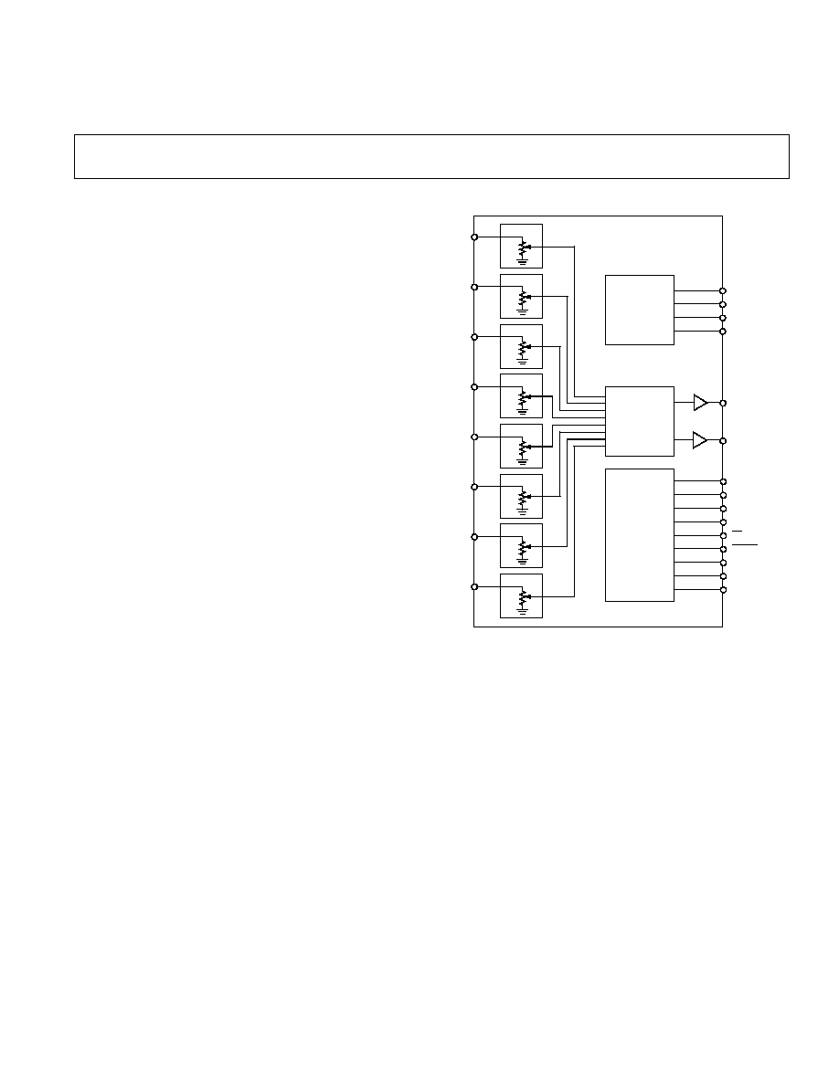
SIMPLIFIED BLOCK DIAGRAM
V
IN1
DCA
V
IN2
DCA
V
IN3
DCA
V
IN4
DCA
V
IN5
DCA
V
IN6
DCA
V
IN7
DCA
V
IN8
DCA
OUTPUT
SWITCHING
NETWORK
VOLTAGE
REFERENCE
GENERATOR
V
CC
V
EE
ACOM
AGND
V
OUTL
V
OUTR
SHIFT
REGISTER
AND
ADDRESS
DECODER
SYSTEM MUTE
DATA OUT
CLK
DATA
LD
WRITE
DGND
V
DD
V
SS
SSM2163
DCA: DIGITALLY CONTROLLED ATTENUATOR

ELECTRICAL SPECIFICATIONS
Parameter
Conditions
Min
Typ
Max
Units
AUDIO PERFORMANCE
Noise
V
IN
= GND, 20 kHz Bandwidth
82
dBu
Headroom
Clip Point = 1% THD+N
+10
dBu
Total Harmonic Distortion Plus Noise
2nd and 3rd Harmonics Only
A
V
= 0 dB
0.007
0.03
%
A
V
= 20 dB
0.02
%
A
V
= 0 dB, V
S
= +5 V, Single Supply
0.035
%
ANALOG INPUT
Input Impedance
7
10
15
k
VOLUME CONTROL
Step Size
1.0
dB
Gain Error
Relative to Same Channel
0 dB Attenuation
0.1
1.0
dB
20 dB Attenuation
0.1
dB
40 dB Attenuation
0.25
Gain Match Error
Channel-to-Channel; Same Level Setting
0 dB Attenuation
0.01
dB
20 dB Attenuation
0.05
dB
40 dB
0.4
dB
Mute Attenuation
64
dB
ANALOG OUTPUT
Output Impedance
15
Output Current
500
µ
A
Minimum Resistive Load
THD = 1%
4
k
Maximum Capacitive Drive
5000
pF
Offset Voltage
Channel Muted
50
mV
CONTROL SECTION
Logic Input LO
0.8
V
Logic Input HI
2.0
V
Logic Input Current
Logic LO or HI
1
µ
A
Logic Out LO
I
OUT
= 0.2 mA
0.4
V
Logic Out HI
I
OUT
= 0.2 mA
2.4
V
Timing Characteristics
See Timing Diagram
REFERENCE (ACOM)
Output Voltage
V
S
= +10 V (Single Supply)
4.7
5.0
5.3
V
Output Impedance
10
Load Regulation
0.5 mA
I
L
+0.5 mA (Single Supply)
0.2
%
POWER SUPPLIES
Supply Voltage Range
Dual Supply
±
4
±
7
V
Single Supply
+5
+14
V
Supply Current
V
S
= +10 V (Single Supply)
8
15
mA
Power Supply Rejection Ratio
Delta Gain
0.005
dB/V
Specifications subject to change without notice.
2
SSM2163SPECIFICATIONS
(V
S
= 5 V, A
V
= 0 dB, V
IN
= 0 dBu = 0.775 V rms, f
AUDIO
= 1 kHz, f
CLK
= 250 kHz, R
L
= 100 k ,
40 C < T
A
< +85 C, unless otherwise noted. Typical specifications apply at T
A
= +25 C.)
REV. 0

SSM2163
REV. 0
3
Timing Description
Timing
Symbol
Description
Min
Typ
Max
Units
t
CL
Input Clock Pulse Width
50
ns
t
CH
Input Clock Pulse Width
50
ns
t
DS
Data Setup Time
25
ns
t
DH
Data Hold Time
35
ns
t
CW
Positive CLK Edge to End of Write
25
ns
t
WC
Write to Clock Setup Time
35
ns
t
LW
End of Load Pulse to Next Write
20
ns
t
WL
End of Write to Start of Load
20
ns
t
L
Load Pulse Width
250
ns
t
W3
Load Pulse Width (3-Wire Mode)
250
ns
t
PD
Propagation Delay from Rising
10
80
160
ns
Clock to SDO Transition
(R
L
= 220 k
, C
L
= 20 pF)
NOTES
1. An idle HI (CLK-HI) or idle LO (CLK-LO) clock may be used. Data is latched on the positive
edge.
2. For SPI or microwire three-wire bus operation, tie LD to WRITE and use WRITE pulse to drive
both pins. (This generates an automatic internal LD signal.)
3. If an idle HI clock is used, t
CW
and t
WL
are measured from the final negative transition to the idle
state.
4. The first data byte selects an address (MSB HI), and subsequent MSB LO states set gain levels. Re-
fer to the Address/Data Decoding Truth Table.
5. Data must be sent MSB first.
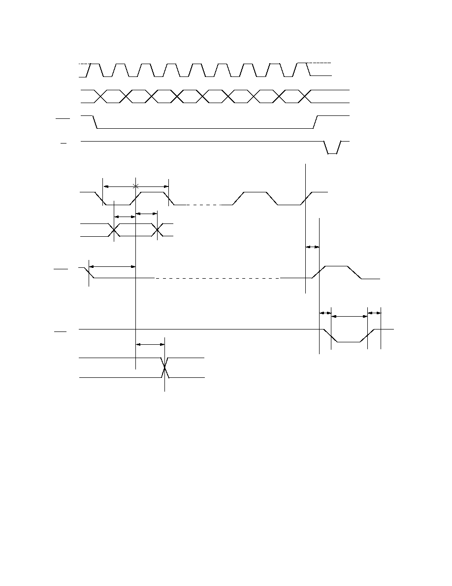
D7
D6
D5
D4
D3
D2
D1
D0
1
0
1
DATA
0
1
0
1
0
1
0
CLK
DATA
t
CL
CLK
1
0
SDO
1
0
t
CH
t
DS
t
DH
t
WC
t
CW
t
PD
t
W3
WRITE
&
LOAD
WRITE
&
LOAD
Figure 1. Three-Wire Mode Timing Diagram
SSM2163
REV. 0
4
D7
D6
D5
D4
D3
D2
D1
D0
1
0
1
0
DATA
WRITE
LD
1
0
1
0
1
0
1
0
CLK
DATA
1
0
t
CL
CLK
1
0
SDO
1
0
WRITE
LOAD
t
CH
t
DS
t
DH
t
WC
t
CW
t
PD
t
WL
t
L
t
LW
Figure 2. Four-Wire Mode Timing Diagram

SSM2163
REV. 0
5
ABSOLUTE MAXIMUM RATINGS
1
Supply Voltage
Dual Supply . . . . . . . . . . . . . . . . . . . . . . . . . . . . . . . . .
±
8 V
Single Supply . . . . . . . . . . . . . . . . . . . . . . . . . . . . . . . +16 V
Analog Input Voltage . . . . . . . . . . . . . . . . . . . . . . . . . . . . .
±
V
S
Logic Input Voltage . . . . . . . . . . . . . . . . . . . . . . . . . . . . . .
±
V
S
Output Current . . . . . . . . . . . . . . . . . . . . . . . . . . . . . . . . 5 mA
Operating Temperature Range . . . . . . . . . . . . 40
°
C to +85
°
C
Storage Temperature . . . . . . . . . . . . . . . . . . 65
°
C to +150
°
C
Junction Temperature (T
J
) . . . . . . . . . . . . . . . . . . . . . +150
°
C
Lead Temperature (Soldering, 60 sec) . . . . . . . . . . . . . +300
°
C
THERMAL CHARACTERISTICS
Thermal Resistance
2
28-Pin Plastic DIP (SSM2163P)
JA
. . . . . . . . . . . . . . . . . . . . . . . . . . . . . . . . . . . . . 48
°
C/W
JC
. . . . . . . . . . . . . . . . . . . . . . . . . . . . . . . . . . . . 22
°
C/W
28-Pin SOIC (SSM2163S)
JA
. . . . . . . . . . . . . . . . . . . . . . . . . . . . . . . . . . . . . 68
°
C/W
JC
. . . . . . . . . . . . . . . . . . . . . . . . . . . . . . . . . . . . 20
°
C/W
TRANSISTOR COUNT
Number of Transistors . . . . . . . . . . . . . . . . . . 1711 MOSFETs
447 BJTs
ESD RATINGS
883 (Human Body) Model . . . . . . . . . . . . . . . . . . . . . . 1000 V
NOTES
1
Stresses above those listed under "Absolute Maximum Ratings" may cause
permanent damage to the device. This is a stress rating only and functional
operation of the device at these or any other conditions above those indicated in the
operation section of this specification is not implied. Exposure to absolute maxi-
mum rating conditions for extended periods may affect device reliability.
2
JA
is specified for worst-case conditions, i.e.,
JA
is specified for device in socket
for P-DIP and device soldered in circuit board for SOIC package.
ORDERING GUIDE
Temperature
Package
Package
Model
Range
Description
Option
SSM2163P
40
°
C to +85
°
C
Plastic DIP
N-28
SSM2163S
40
°
C to +85
°
C
SOIC
R-28
PIN CONFIGURATIONS
Epoxy Plastic DIP (P-Suffix)
and SOIC (S-Suffix)
14
13
12
11
17
16
15
20
19
18
10
9
8
1
2
3
4
7
6
5
28
27
26
25
24
23
22
21
TOP VIEW
(Not to Scale)
SSM2163
DGND
WRITE
CLK
DATA IN
SYSTEM MUTE
V
SS
DATA OUT
V
DD
V
IN2
NC (SHIELD)
LD
V
IN1
NC (SHIELD)
V
IN3
NC (SHIELD)
V
IN5
V
CC
NC (SHIELD)
V
IN4
NC (SHIELD)
V
IN7
V
EE
ACOM
V
OUTL
V
IN6
V
OUTR
V
IN8
AGND
CAUTION
ESD (electrostatic discharge) sensitive device. Electrostatic charges as high as 4000 V readily
accumulate on the human body and test equipment and can discharge without detection.
Although the SSM2163 features proprietary ESD protection circuitry, permanent damage may
occur on devices subjected to high energy electrostatic discharges. Therefore, proper ESD
precautions are recommended to avoid performance degradation or loss of functionality.
WARNING!
ESD SENSITIVE DEVICE
SSM2163
REV. 0
6
PIN DESCRIPTION
Pin #
Mnemonic
Function
1
DGND
Digital Ground.
2
V
SS
Digital Negative Supply.
3
DATA OUT
Serial data output clocked on positive clock edge. Connect DATA OUT to DATA IN pin to
daisy-chain multiple SSM2163s. Output levels are V
DD
to DGND.
4
V
DD
Digital Positive Supply.
5
V
IN1
Audio Signal Input 1.
6
NC (Shield)
Shield Pin. Should be tied to AGND to minimize crosstalk.
7
V
IN3
Audio Signal Input 3.
8
NC (Shield)
Shield Pin. Should be tied to AGND to minimize crosstalk.
9
V
IN5
Audio Signal Input 5.
10
V
CC
Analog Positive Supply.
11
V
IN7
Audio Signal Input 7.
12
V
EE
Analog Negative Supply.
13
ACOM
Analog Common Voltage. Provides a buffered voltage output halfway between V
CC
and V
EE
for use
as a pseudo ground in single supply applications.
14
V
OUTL
Left Audio Output.
15
V
OUTR
Right Audio Output.
16
V
IN8
Audio Signal Input 8.
17
AGND
Analog Ground.
18
V
IN6
Audio Signal Input 6.
19
NC (Shield)
Shield Pin. Should be tied to AGND to minimize crosstalk.
20
V
IN4
Audio Signal Input 4.
21
NC (Shield)
Shield Pin. Should be tied to AGND to minimize crosstalk.
22
V
IN2
Audio Signal Input 2.
23
NC (Shield)
Shield Pin. Should be tied to AGND to minimize crosstalk.
24
LD
Load Data.
25
WRITE
Write Data.
26
CLK
Clock.
27
Data In
Serial Data Input. Clocked on positive clock edge.
28
SYSTEM MUTE
Mutes all eight input channels thus left and right audio output are muted. System mute does not
change the state of internal latches. All digital data remains intact after system mute is applied.
Logic One: Mutes Output
Logic Zero: Normal Operation
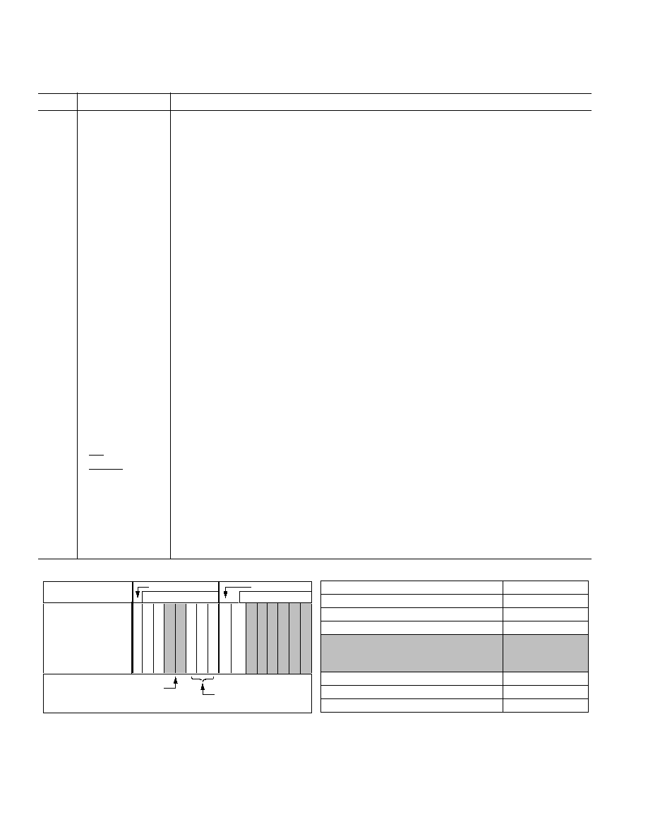
DATA
ATTENUATION
0
0
0
1
1
1
0
0
0
0
0
0
0
0
0
0
0
1
0
1
0
1
1
1
1
1
1
1
1
1
0
1
1
1
0
1
.
.
.
.
.
.
.
.
.
.
.
.
.
.
.
.
.
.
.
.
.
.
.
.
.
.
.
.
0dB
1dB
2dB
61dB
62dB
63dB
0
0
0
0
0
0
0
0
1
1
1
1
1
1
1
1
X
X
X
X
X
X
X
X
X
X
X
X
X
X
X
X
0
0
1
1
0
0
1
1
0
1
0
1
0
1
0
1
INPUT CHANNEL 1
INPUT CHANNEL 2
INPUT CHANNEL 3
INPUT CHANNEL 4
INPUT CHANNEL 5
INPUT CHANNEL 6
INPUT CHANNEL 7
INPUT CHANNEL 8
DATA MODE
ADDRESS MODE
DATA
ADDRESS
SELECTION
X = "DON'T CARE," SHADED AREA IS DATA
MSB
LSB
MSB
LSB
X
X
X
X
X
X
X
X
R
I
G
H
T
L
E
F
T
OUTPUT SELECT
1 = SELECTED, 0 = NOT SELECTED
INPUT SELECT
0
0
0
0
1
1
1
1
Figure 3. Address and Data Decoding Truth Table
SSM2163
REV. 0
7
FREQUENCY Hz
20.000
10.000
80.00
20
20k
0.0
AMPLITUDE dBr
100
10.00
20.00
30.00
1k
50.00
60.00
10k
40.00
70.00
A
V
= 0dB
A
V
= 20dB
A
V
= 40dB
V
S
=
±
5V
LPF = 22kHz
R
L
= 100k
T
A
= +25
°
C
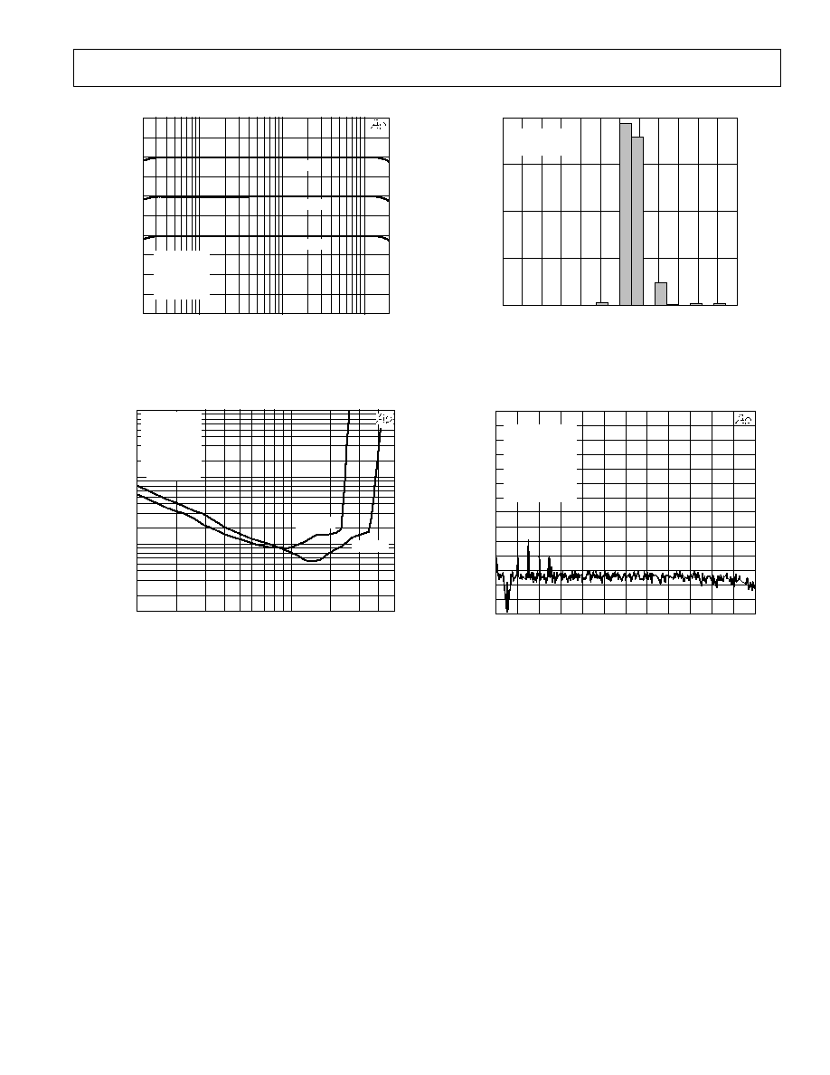
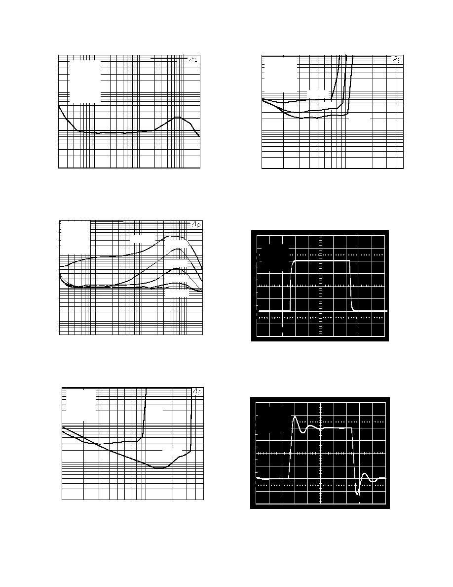
Figure 4. Frequency Response
AMPLITUDE V rms
0.001
0.1
5
THD + N %
1
1
0.1
V
S
=
±
5V
V
S
=
±
7V
0.010
A
V
= 0dB
FREQ = 1kHz
LPF = 22kHz
R
L
= 100k
T
A
= +25
°
C
Figure 5. THD+N vs. Amplitude
THD %
1400
1050
0
0.0
0.012
UNITS
0.002
0.004
0.006
0.008
0.010
700
350
V
S
=
±
5V
T
A
= +25
°
C
Figure 6. THD Distribution
FREQUENCY kHz
0
20
2
4
6
8
10
12
14
16
18
0
10
dBu
20
30
40
50
60
70
80
90
100
110
120
130
140
22
24
V
S
=
±
5V
V
IN
= 0dBu
A
V
= 0dB
Notch F = 1kHz
R
L
= 100k
T
A
= +25
°
C
Figure 7. (THD+N) = 1 kHz Tone at 0 dBu (4k-Point FFT)
SSM2163
REV. 0
8
FREQUENCY Hz
0.001
20
20k
THD + N %
100
1
0.1
0.010
1k
10k
V
S
=
±
5V
V
IN
= 0dBu
A
V
= 0dB
LPF = 22kHz
R
L
= 100k
T
A
= +25
°
C
Figure 8. THD+N vs. Frequency
FREQUENCY Hz
0.001
20
20k
THD + N %
100
1
0.1
0.010
V
IN
= 0dBu
A
V
= 0dB
LPF = 22kHz
R
L
= 100k
T
A
= +25
°
C
1k
10k
0.005
V
S
= 4.5V
V
S
= 5V
V
S
= 7V
V
S
= 10V
V
S
= 12V
Figure 9. THD+N vs. Frequency Single Supply
AMPLITUDE V rms
0.001
0.1
5
THD + N %
1
1
0.1
0.010
V
S
= 5V
A
V
= 0dB
FREQ = 1kHz
LPF = 22kHz
R
L
= 100k
T
A
= +25
°
C
V
S
= 14V
Figure 10. THD+N vs. Amplitude Single Supply
AMPLITUDE V rms
0.001
0.1
5
THD + N %
1
1
0.1
0.010
V
S
= 4.5V
V
S
= 5V
V
S
= 5.5V
A
V
= 0dB
FREQ = 1kHz
LPF = 22kHz
R
L
= 100k
T
A
= +25
°
C
Figure 11. THD+N vs. Amplitude Single Supply
10
0%
100
90
10µS
50mV
V
S
=
±
5V
A
V
= 1
NO LOAD
T
A
= +25
°
C
Figure 12. Small Signal Transient Response
10
0%
100
90
10µS
50mV
V
S
=
±
5V
A
V
= 1
C
L
= 10,000pF
T
A
= +25
°
C
Figure 13. Small Signal Transient Response
SSM2163
REV. 0
9
10
0%
100
90
1µS
1V
V
S
=
±
5V
NO LOAD
T
A
= +25
°
C
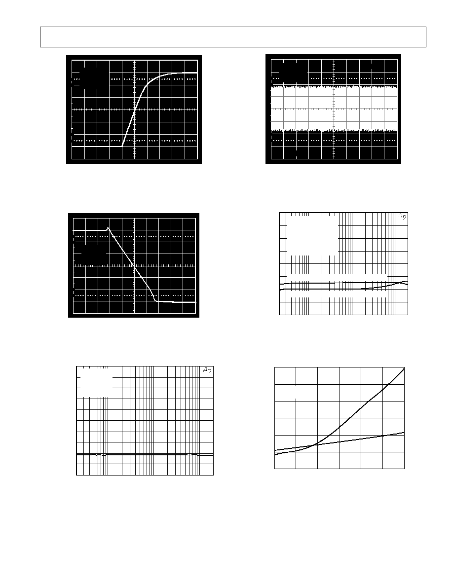
Figure 14. Large Signal Transient Response
10
0%
100
90
1µS
1V
V
S
=
±
5V
NO LOAD
T
A
= +25
°
C
Figure 15. Large Signal Transient Response
FREQUENCY Hz
0.0
10.00
20
20k
20.00
AMPLITUDE dBr
100
30.00
40.00
50.00
1k
70.00
80.00
10k
60.00
90.00
100.00
V
S
=
±
5V
LPF = 22kHz
R
L
= 100k
T
A
= +25
°
C
Figure 16. Noise Amplitude vs. Frequency
10
0%
100
90
50mS
20mV
V
S
=
±
5V
T
A
= +25
°
C
A
V
= 100
Figure 17. Broadband Noise
FREQUENCY Hz
0.0
10.00
20
20k
20.00
AMPLITUDE dBr
100
30.00
40.00
50.00
1k
70.00
80.00
10k
60.00
V
S
=
±
5V
V
IN
= CHANNEL 1 0dBu
A
V
= 0dB
LPF = 22kHz
R
L
= 100k
T
A
= +25
°
C
RIGHT OUTPUT WITH V
IN
STEERED FULL LEFT
LEFT OUTPUT WITH V
IN
STEERED FULL RIGHT
Figure 18. Output Channel Separation vs. Frequency
30
25
20
15
10
5
0
SUPPLY CURRENT mA
4
4.5
5
5.5
6
6.5
7
SUPPLY VOLTAGE
±
V
T
A
= +25
°
C
R
L
= 100k
ISY+
ISY
Figure 19. Supply Current vs. Supply Voltage
SSM2163
REV. 0
10
THEORY OF OPERATION
The SSM2163 is an eight-input, two-output audio mixer and
attenuator. The device provides eight analog inputs, each of
which can be individually attenuated by 0 dB to 63 dB in 1 dB
steps (see the SSM2163 simplified block diagram). The eight
signals can then be mixed into one or both of two analog
outputs. The channel attenuation level and mixer functions
are controlled by digital registers, which are loaded via a
serial interface. A hardware mute input is included to
asynchronously force all inputs into the muted state.
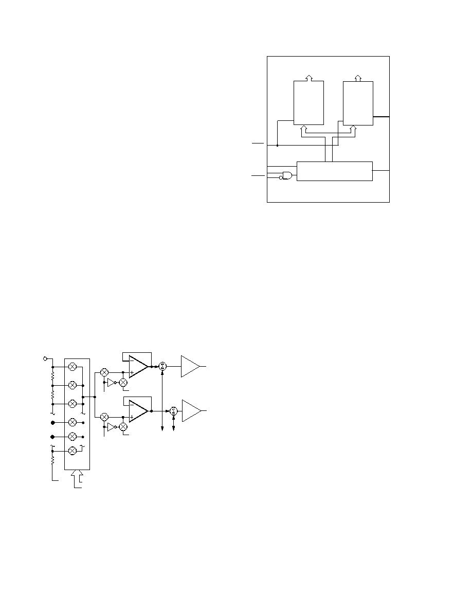
Analog Section
The analog signal path is shown in Figure 20. Each analog input
has a nominal impedance of 10 k
. Each input therefore
appears as a digitally programmable 10 k
potentiometer. The
SSM2163 input impedance remains constant as the attenuation
level changes. Therefore, the sources which drive the SSM2163
do not have to drive complex and variable impedances.
The attenuated analog input is applied to the left and right
channel inputs of the mixer. Each mixer channel consists of an
analog switch and a buffer amplifier. If the channel is selected
(via the appropriate bit in the mixer control register), the analog
switch is turned on. The buffer amplifier is included after the
analog switch so that the gain of each channel will not be
affected by the potentiometer setting or by the on-resistance
(RDS(ON)) of the switch.
Each mixer channel which is ON is then summed into its
respective (Left or Right) mixer summing amplifier. (If both of
the mixer channels are ON, then the attenuated analog input
will be applied to both the Left and Right summing amplifiers.)
The buffered output of the summing amplifier will supply
±
500
µ
A to an external load.
R1
R2
V
IN1
R63
AGND
1 OF 63
DECODER
ATTENTION VALUE
FROM DATA REGISTER
NOTE: ONLY ONE OF EIGHT CHANNELS
SHOWN FOR CLARITY
ATTENUATOR
AGND
AGND
CH1L
SELECT
CH1R
SELECT
MIXER
SWITCH
MIXER
BUFFER AMP
TO INPUTS
V
IN2
V
IN8
K = 1
K = 1
V
OUTL
V
OUTR
OUTPUT
BUFFER
SUMMING
AMPLIFIER
Figure 20. SSM2163 Analog Signal Path
Digital Interface
The digital interface consists of two banks of 8 data registers
with a serial interface (Figure 21). One register bank holds the
left/right mixer control bits, while the other register bank holds
the 6-bit attenuator value.
TO ATTENUATOR
SWITCHES
TO MIXER
SWITCHES
ATTENUATOR
LEVEL
DATA
LATCHES
(6 BITS)
LEFT/RIGHT
CHANNEL
CONTROL
LATCHES
(2 BITS)
RESET
MUTE
INPUT
DATA
CLOCK
INPUT SHIFT REGISTER
SERIAL DATA
OUTPUT
LOAD
CLK
CLK
DATA IN
CLK
WRITE
Figure 21. SSM2163 Serial Data Interface Block Diagram
To access the SSM2163, the host controller (typically a micro-
computer) writes a value to the serial shift register which selects
the appropriate input channel register for subsequent attenuator-
load operations. This write operation also controls the left and
right mixer switches. The next write operation then loads the
6-bit attenuator level into the appropriate register. If a series of
values are going to be written to the same address, for instance
when fading a channel, then only one write operation to the
address register is required.
Serial Data Control Inputs
The SSM2163 provides a simple 3- or 4-wire serial interface
(Figures 22 and 23). Data is input on the DATA IN pin, while
CLK is the serial clock. Data can be shifted into the SSM2163
clock rates up to 1 MHz.
The shift register clock, CLK, is enabled when the WRITE
input is low. The WRITE pin can therefore be used as a chip
select input. However, the shift register contents are not
transferred to the register banks until the rising edge of LOAD.
In most cases, WRITE and LOAD will be tied together, forming
a traditional 3-wire serial interface. See the Microcomputer
Interfaces section of this data sheet for more information.
To enable a data transfer, the WRITE and LOAD inputs are
driven low. The 8-bit serial data, formatted MSB first, is input
on the DATA IN input and clocked into the shift register on the
rising edge of CLK. The data is latched on the rising edge of
WRITE and LOAD. If the data is an address, then the mixer
control is updated. If the data is an attenuator value the rising
edge of WRITE and LOAD will update the appropriate
attenuator value.
MUTE Input
The MUTE pin provides a hardware input to force all the
SSM2163 channels into the muted state. The MUTE input is
active HIGH. Most
µ
C I/O pins are in a high impedance state or
configured as inputs at power-up, so the SSM2163 will
automatically be muted at power-up. A 10 k
resistor to +5 V is
recommended, to ensure that MUTE is pulled high reliably.
The MUTE input can also be driven from a
µ
C's RESET signal
to force a power-on mute.
In addition to power-on, the MUTE input can be used to
asynchronously mute all channels at any time. The mute
function of the SSM2163 does not affect the attenuator values
SSM2163
REV. 0
11
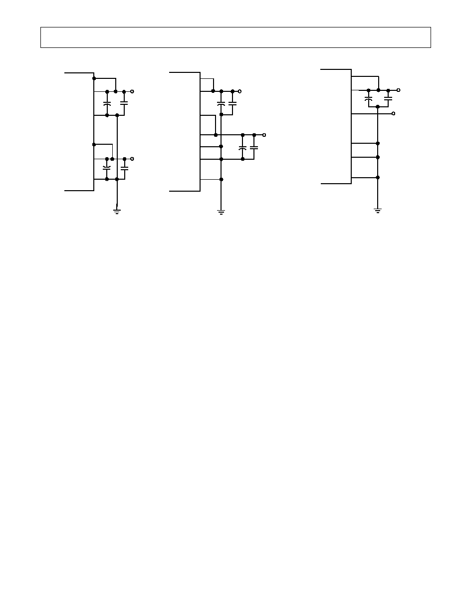
SSM2163 power supply connections
Power Supplies and Decoupling
The SSM2163 operates from either single or dual (split) power
supplies. In either case, proper supply decoupling is important
to maximize audio performance.
To reduce noise, separate pins are provided for the digital and
analog power supply connections. These pins should be
connected together (V
DD
to V
CC
and V
EE
to V
SS
) as close to the
SSM2163 package as possible (Figures 22a, 22b, 22c, power
supply connections).
Single Supply Operation
The SSM2163 will operate with a single power supply of +5 V
to +14 V. Single supply operation simplifies design and reduces
system cost in multimedia applications, battery powered
systems, and similar designs. The SSM2163 provides about
2 dB of headroom (to 1% THD+N) when operating from a
single +5 V supply.
The key to operating from a single supply is to reference all
analog common connections to a voltage midway between the
supply and ground. To simplify single supply operation, the
SSM2163 provides a buffered pseudo-ground reference (ACOM)
on Pin 13. This reference, shown in Figure 23, provides a low
impedance output at approximately one half of the supply
voltage. Connect Analog Ground (Pin 17) to the ACOM output
(Pin 13) for single supply operation. To minimize noise caused
by modulation of the pseudo-ground, Pin 13 should be bypassed to
power supply ground with 0.1
µ
F and 10
µ
F capacitors.
stored in the attenuator control registers. To re-enable the
system after a mute, use the address byte to turn on the desired
mixer channel. The selected channel will then operate with the
previously set attenuator value.
Serial Data Input Format
As previously mentioned, data is written to the SSM2163 in two
8-bit bytes. The serial data format is shown in the Address and
Data Decoding Truth Table, Figure 3. The first byte sent contains
the channel address and the Left/Right output mixer control bits.
The address byte is identified by the MSB being high.
The second byte contains the data (i.e., the attenuator value).
The six LSBs of this byte set the attenuation level, from 0 dB to
63 dB. The MSB of the data byte must be a logic zero.
The standard format for data sent to the SSM2163 is an address
byte followed by a data (attenuator level) byte. In some cases,
however, only one byte needs to be sent. For example,
attenuation levels are not affected by the MUTE input. To turn
a muted channel on, simply send an address byte with the Left
or Right mixer bit set. The addressed channel will immediately
be enabled, using the previously-set attenuation level.
Furthermore, once a channel is addressed the attenuation level
can be varied by sending additional data bytes. For example,
fading a channel can be accomplished by simply incrementing
the data value sent to the SSM2163.
Serial Data Output
The MSB of the shift register is available on the serial DATA
OUTPUT pin. This output can be connected to the input of
another SSM2163 to permit "daisy-chain" operation. See
Figure 26 for a typical application. The DATA OUTPUT pin
swings between the digital power supply rails (i.e., from V
DD
to
V
SS
).
Logic Levels
All of the SSM2163 logic inputs have TTL and CMOS
compatible thresholds. However, the allowable voltage range
for these inputs extends from V
DD
to V
SS
.
(NC)
10
17
12
1
AGND
DGND
V+
EXTERNAL
REFERENCE
0.1
µ
F
10
µ
F
+
V
CC
V
EE
ACOM
2
V
SS
V
DD
4
Figure 22c. Single Supply Using External
Reference
10
17
12
1
V
CC
AGND
V
EE
DGND
V+
VREF
OUT
13
0.1
µ
F
10
µ
F
+
0.1
µ
F
10
µ
F
+
ACOM
2
V
SS
V
DD
4
Figure 22b. Single Supply
10
17
12
1
AGND
ACOM
DGND
V+
V
(NC)
0.1
µ
F
10
µ
F
+
0.1
µ
F
10
µ
F
+
V
CC
V
EE
4
2
V
SS
V
DD
Figure 22a. Dual Supply

SSM2163
REV. 0
12
V
CC
V
DD
AGND
ACOM
DGND
V
EE
V
SS
SSM2163
TTL/CMOS
LOGIC
CIRCUITS
+5V
POWER
SUPPLY
+5V
GND
10
µ
F
0.1
µ
F
0.1
µ
F
10
µ
F
+
+
Figure 24. Use Separate Traces to Reduce Power Supply
Noise
Even if the system includes separate analog and digital power
supplies, both the analog and digital power pins of the
SSM2163 should be connected to the analog supply. While this
connection will inject a small amount of digital noise into the
analog ground, the effect is small due to the SSM2163's low
digital logic input currents and capacitances. If, on the other
hand, the SSM2163's digital supply pins are connected to a
digital power supply, then noise from the digital supply will be
coupled into the SSM2163 and degrade performance.
APPLICATIONS
An 8-Input, 2-Output Mixer
A single-chip, 8-input, 2-output mixer using the SSM2163 is
shown in Figure 25. With this circuit, any of the eight channels
can be attenuated by 0 dB to 63 dB and mixed into the right,
left, or both outputs under software control.
10µF
10µF
10µF
10µF
10µF
10µF
10µF
10µF
+
+
+
+
+
+
+
+
5
22
7
20
9
18
11
16
27
26
25
24
28
14
15
3
NC
4
10
+5V
+
10µF
0.1µF
LEFT CHANNEL
OUTPUT
RIGHT CHANNEL
OUTPUT
V
IN1
V
DD
V
CC
V
OUTL
V
OUTR
DATA OUT
SHIELD
SHIELD
SHIELD
SHIELD
SHIELD
AGND
ACOM
DGND
V
SS
V
EE
2
12
1
6
8
19
21
23
17
13
10µF
0.1µF
+
V
IN2
V
IN3
V
IN4
V
IN5
V
IN6
V
IN7
V
IN8
DATA IN
CLK
WRITE
LD
SYSMUTE
SSM2163
INPUT 1 LEFT
INPUT 2 LEFT
INPUT 3 LEFT
INPUT 4 LEFT
INPUT 1 RIGHT
INPUT 2 RIGHT
INPUT 3 RIGHT
INPUT 4 RIGHT
DATA IN
CLOCK
CHIP SELECT
SYSTEM MUTE
Figure 25. An 8-Input, 2-Output Mixer
This circuit demonstrates ac coupling of the inputs. As
previously mentioned, this eliminates level shifting concerns
from previous stages.
The circuit of Figure 25 also demonstrates single +5 V supply
operation. The output of the ACOM supply-splitter, Pin 13,
provides the pseudo-ground reference which is required when
operating from a single supply.
ATTENUATOR
MIXER
SWITCH
CHANNEL
SELECT
MIXER
BUFFER AMP
AGND
MIXER SUMMING
AMPLIFIER
V
OUT
V
IN
V
OUT
V
CC
R1
R2
V
EE
R1=R2
ACOM
10µF
0.1µF
V
EE
Figure 23. Single-Supply Pseudo-Ground Reference
(ACOM) Generator
For single supply operation, the inputs can either be ac-coupled,
as shown in Figure 25, or referenced to the pseudo-ground out-
put. AC coupling eliminates dc offset and offset drift
differentials between the input source and the SSM2163. In
addition, ac coupling reduces the risk of "clicks" when switching
between multiple dc-coupled inputs which have different
reference levels.
Since the input coupling capacitors are in series with the 10 k
input of the attenuator, the impedance of these capacitors will
influence low frequency gain. The inexpensive 10
µ
F aluminum
electrolytic capacitors shown will limit the gain error to 0.66 dB
at 20 Hz.
If the entire system is operating from a single supply, then
typically the input voltage is already referenced to the midpoint
of the supply. In this case, the SSM2163 can be referenced to
the same midpoint reference source, as shown in Figure 22c.
This connection will eliminate dc offset errors caused by having
the input signal common and the SSM2163 analog common
referenced to different voltages. DC offset errors can also be
eliminated, of course, by using the ac coupling technique
discussed above.
Dual-Supply Operation
The SSM2163 will also operate from dual supplies, ranging
from
±
4 V to
±
7 V. (See Figure 22a.) In this case, input signals
can be referenced to power supply ground. The ACOM output
(Pin 13) is left open (no connection) for dual supply operation.
Supply Decoupling
Optimizing the performance of the SSM2163, or any low noise
device, requires careful attention to power supply decoupling.
Since the SSM2163 can operate from a single +5 V supply, it
seems convenient to simply tap into the digital logic power
supply. Unfortunately, the logic supply is often a switch-mode
design, which generates noise in the 20 kHz to 1 MHz range. In
addition, fast logic gates can generate glitches hundred of millivolts
in amplitude due to wiring resistances and inductances.
If a separate analog power supply is not available, the SSM2163
can be powered directly from the system power supply. Separate
power and ground traces should be provided for the analog
section, if possible. This arrangement, shown in Figure 24, will
isolate the analog section from the logic switching transients.
Even if a separate power supply trace is not available, however,
generous supply bypassing will reduce supply line induced
noise. Local supply bypassing, consisting of a 10
µ
F tantalum
electrolytic in parallel with a 0.1
µ
F ceramic capacitor, is
recommended in all applications. (See the SSM2163 Power
Supply Connections figures.)
SSM2163
REV. 0
13
The circuit of Figure 26 illustrates dc coupling of the inputs.
DC coupling is practical with dual supplies and ground-
referenced inputs, because the dc offsets associated with single-
supply operation are reduced. However, ac coupling could also
be used, and employing both ac- and dc-coupled signals in one
mixer is also possible. In addition, this circuit illustrates the
connections for
±
5 V power supplies. Note that the negative
supply, as well as the positive supply, should be bypassed to
ground.
Implementing a Software-Controlled Pan-Pot
Pan and fade effects are important attributes of modern multi-
media presentations and similar applications. One way to
achieve these effects is to apply the input signal to two input
channels of the SSM2163, as shown in Figure 27. Since any
input channel can be mixed into either or both outputs,
sophisticated pan and fade effects are easily accomplished in
software. For example, Input 1 can be connected to the left
channel with 0 dB attenuation, while Input 2 is applied to the
right channel with 10 dB of attenuation. This configuration
will produce the effect of having the audio source "located" to
the left of center line of the speakers. Another possible option
would be to attenuate the left channel while boosting the right,
which would produce an effect of movement of the audio source.
Since any input can be connected to either output, very flexible
and sophisticated effects can be produced without hardware
changes.
V
OUTL
V
OUTR
V
IN2
V
IN1
V
IN
SSM2163
TO INPUTS
V
IN3
V
IN8
Figure 27. Connecting the SSM2163 for Pan-Pot
Operation
Driving Headphones
A high speed, high output current amplifier, such as the OP279,
can be added to drive headphones directly. A typical connection
is shown in Figure 28. Single +5 V operation is maintained,
since the OP279 offers rail-to-rail inputs and outputs. The
OP279's high current output stage can drive a 48
load to
4 V p-p while maintaining less than 1% THD.
Mixing Additional Channels
Some mixing applications require more than four inputs for
each stereo channel. To meet the requirements of these systems,
two or more SSM2163s can be paralleled to provide additional
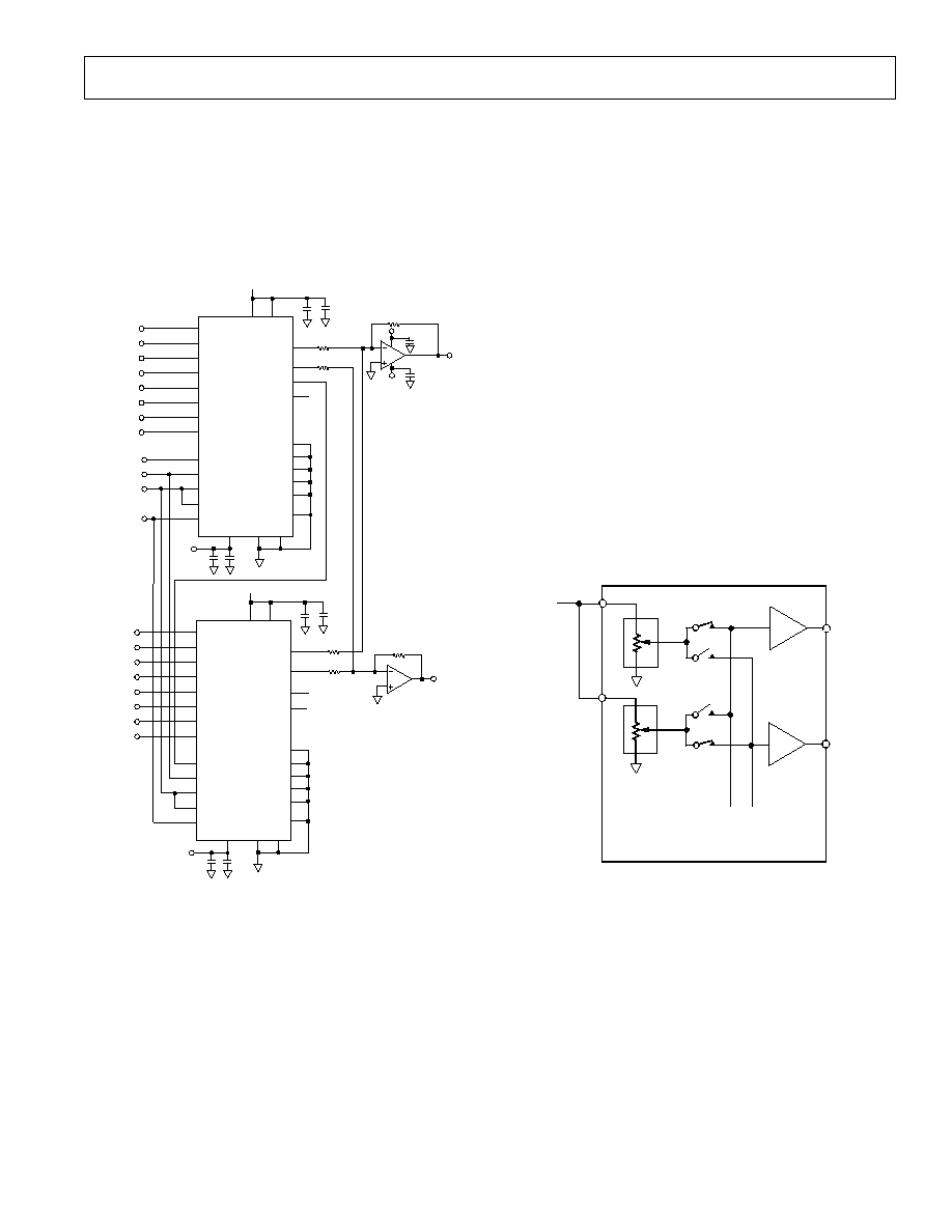
channels. A typical circuit is shown in Figure 26, which combines
two SSM2163s to form a 16-input, 2-output mixer. An SSM2135
dual audio op amp sums the outputs of each of the SSM2163s.
With this system, any of the 16 inputs can be mixed into either
or both of the output channels.
5
22
7
20
9
18
11
16
27
26
25
24
28
14
15
3
NC
4
10
+5V
+
10µF
0.1µF
V
DD
V
CC
V
OUTL
V
OUTR
DATA OUT
SHIELD
SHIELD
SHIELD
SHIELD
SHIELD
AGND
ACOM
DGND
V
SS
V
EE
2
12
1
6
8
19
21
23
17
13
10µF
0.1µF
+
V
IN2
V
IN3
V
IN4
V
IN5
V
IN6
V
IN7
V
IN8
DATA IN
CLK
WRITE
LD
SYSMUTE
SSM2163
DATA IN
CLOCK
CHIP SELECT
SYSTEM MUTE
5
22
7
20
9
18
11
16
27
26
25
24
28
14
15
3
NC
4
10
+5V
+
10µF
0.1µF
V
DD
V
CC
V
OUTL
V
OUTR
DATA OUT
SHIELD
SHIELD
SHIELD
SHIELD
SHIELD
AGND
ACOM
DGND
V
SS
V
EE
2
12
1
6
8
19
21
23
17
13
DATA IN
CLK
WRITE
LD
SYSMUTE
SSM2163
V
IN1
V
IN2
V
IN3
V
IN4
V
IN5
V
IN6
V
IN7
V
IN8
5V
#1
#2
V
IN1
V
IN2
V
IN3
V
IN4
V
IN5
V
IN6
V
IN7
V
IN8
10µF
0.1µF
+
5V
NC
20k
+5V
0.1µF
0.1µF
5V
20k
20k
1/2 SSM2135
V
OUTL
20k
1/2 SSM2135
V
OUTR
20k
20k
V
IN1
V
IN1
V
IN2
V
IN3
V
IN4
V
IN5
V
IN6
V
IN7
V
IN8
Figure 26. A 16-Input, 2-Output Mixer
This circuit utilizes the DATA OUT feature of the SSM2163 to
transfer data from the first SSM2163 to the second. In the
daisy-chain mode, the DATA OUT pin of the first SSM2163 is
connected to the DATA IN pin of the second device. The
advantage of this "daisy chain" connection is that it allows a
3-wire serial interface, as was used in the previous 8-input
mixer, to control two or more SSM2163s.
The serial data format for the daisy chain circuit is similar to the
8-channel application, except that the SSM2163s are loaded in
tandem. After setting WRITE and LOAD low, two bytes (16 bits)
are clocked into the first SSM2163. When WRITE and
LOAD return high, data will be latched into both SSM2163s
simultaneously.
SSM2163
REV. 0
14
SSM2163
V
OUTL
V
OUTR
14
15
+V +5V
1/2
OP279
1/2
OP279
16
16
+
+
220µF
220µF
50k
50k
LEFT
HEADPHONE
RIGHT
HEADPHONE
Figure 28. A Single-Supply Stereo Headphone Driver
The op amp's input offset voltage is only 4 mV maximum, so
the SSM2163 output can be dc coupled. The headphone output
is ac coupled through a 220
µ
F capacitor. The large coupling
capacitor is required because of the low impedance of the
headphones, which can range from 32
to 600
. An additional
16
resistor is used in series with the output capacitor to protect
the op amp's output stage by limiting capacitor discharge current.
Microcomputer Interfaces
The SSM2163 serial data input provides an easy interface to a
variety of single chip microcomputers (
µ
Cs). Many
µ
Cs have a
built-in serial data capability which can be used for
communicating with the SSM2163. In cases where no serial
port is provided, or it is being used for some other purpose
(such as an RS-232 communications interface), the SSM2163
can easily be addressed in software.
The SSM2163 can operate in either a 3-wire or 4-wire mode.
In most cases, the 3-wire mode is more practical, due to
reduced PC board traces and compatibility with
µ
C serial
interface protocols. A typical interface, using the 80C51
µ
C, is
shown in Figure 29, while the interface waveforms are shown in
the Timing Diagram, 3-Wire Mode, Figure 1.
(P3.0) RxD
(P3.1) TxD
P1.4
P1.3
80C51 µC
+5V
10k
DATA IN
CLK
WRITE
LD
SYSMUTE
SSM2163
NOTE: ADDITIONAL PINS OMITTED FOR CLARITY
Figure 29. Interfacing the 80C51
µ
C to an SSM2163 in
3-Wire Mode
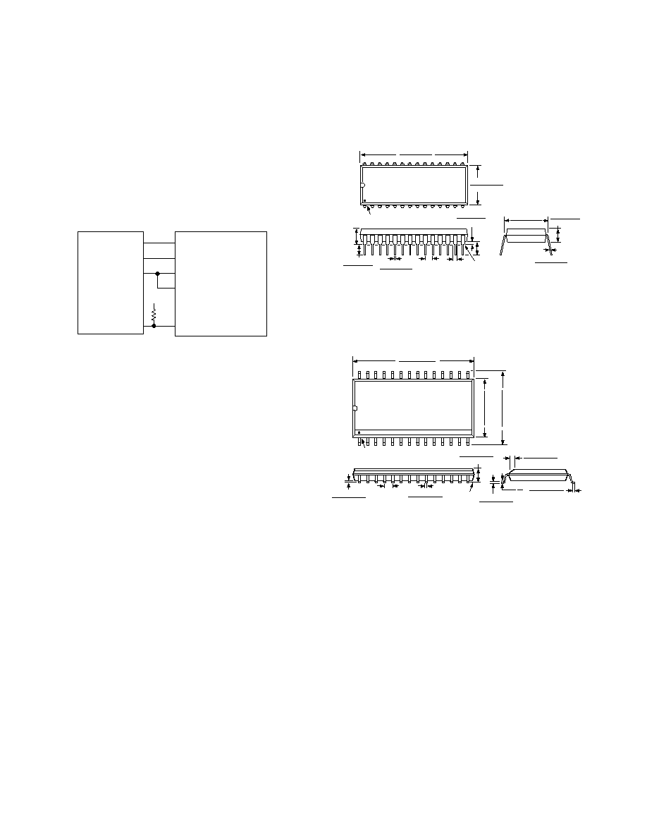
Port in 4-Wire Mode
In some cases, it may be desirable to synchronize the outputs of
several SSM2163s. The 4-wire mode, shown in Figure 30,
provides this capability. As shown in Figure 2, the Timing
Diagram, 4-Wire Mode, the input shift register is loaded with
data while the WRITE input is low. However, the data will not
be latched into the SSM2163's internal registers until the
rising edge of the LOAD input. In this manner, any number
of SSM2163s can be loaded with data, while the amplitude and
mixer changes will not occur until the separate LOAD pulse
occurs.
(P3.0) RxD
(P3.1) TxD
P1.4
P1.3
80C51 µC
+5V
10k
DATA IN
CLK
WRITE
LD
SYSMUTE
SSM2163
NOTE: ADDITIONAL PINS OMITTED FOR CLARITY
P1.2
Figure 30. Interfacing the 80C51
µ
C to an SSM2163 in
4-Wire Mode
An 80C51 C Interface
A typical interface between the SSM2163 and an 80C51
µ
C is
shown in Figure 30. This interface uses the 80C51's internal
serial port. The serial port is programmed for Mode 0 operation,
which functions as a simple 8-bit shift register. The 80C51's Port
3.0 pin functions as the serial data output, while Port 3.1 serves
as the serial clock.
When data is written to the serial buffer register (SBUF, at
Special Function Register location 99H), the data is
automatically converted to serial format and clocked out via
Port 3.0 and Port 3.1. After 8 bits have been transmitted, the
Transmit Interrupt flag (SCON.1) is set and the next 8 bits
can be transmitted.
The 80C51 transmits serial data in Least Significant Bit (LSB)-
first format. The SSM2163, on the other hand, requires data in
MSB format. A BYTESWAP routine swaps the order of the bits
before transmission.
The SSM2163 requires the Chip Select to go low at the begin-
ning of the serial data transfer. After each 8 bits (either address
or attenuation value) are transmitted, Chip Select must go high
to latch data into the appropriate register. Chip Select is controlled
by the 80C51's port 1.4 pin.
Software for the 80C51 Interface
A software routine for the SSM2163 to 80C51 interface is
shown in Listing 1. The routine transfers the 6-bit attenuation
level stored at data memory location LEVEL_VALUE to the
SSM2163 input addressed by the contents of location
INPUT_ADDR, and turns the Left and/or Right mixer channels
on/off based on bits 3 and 4 of INPUT_ADDR.

SSM2163
REV. 0
15
The 80C51 sends data out of its shift register LSB first, while
the SSM2163 requires data MSB first. The subroutine therefore
includes a BYTESWAP subroutine to reformat the data. This
routine transfers the MSB-first byte at location SHIFTREG to
an LSB-first byte at location SENDBYTE. The routine rotates
the MSB of the first byte into the carry with a Rotate Left
Carry instruction, then rotates the carry into the MSB of the
second byte with a Rotate Right Carry instruction. After 8
loops, SENDBYTE contains the data in the proper format.
The BYTESWAP routine in Listing 1 is convenient because the
attenuator data can be calculated in normal LSB form. For
example, fading a channel on the SSM2163 is simply a matter
of repeatedly incrementing the LEVEL_VALUE location and
calling the SEND_VAL subroutine. (Remember, the 6-bit
Listing 1. Software for the 80C51-SSM2163 Serial Port Interface
; This subroutine loads an SSM2163 mixer channel with a 6-bit
; attenuator value, and turns the Left or Right mixer switch ON or OFF.
; The attenuator value is stored at location ATTEN_VALUE
; The mixer channel address is stored at location INPUT_ADDR
;
PORT1
DATA
90H
;SFR register for port 1
ATTEN_VALUE
DATA
40H
;Attenuation level (0=0dB)
;ATTEN-VALUE: B7=0, B5B0=Attenuation Value
INPUT_ADDR
DATA
41H
;Mixer Channel Address
;INPUT_ADDR: B7=1, B4=L chnl, B3=R chnl, B2-B0=address
LOOPCOUNT
DATA
42H
;Count loops for byte swap
SHIFTREG
DATA
43H
;Shift reg. for byte swap
SENDBYTE
DATA
44H
;Destination reg. for byte swap
;
ORG
100H
;arbitrary starting address
LD_2163:
CLR
SCON.7
;set serial
CLR
SCON.6
; data mode 0
CLR
SCON.5
;Clr SM2 for mode 0
CLR
SCON.1
;clr the transmit flag
CLR
PORT1.3
;Mute function off
SETB
PORT1.4
;WRITE and LOAD High
MOV
SHIFTREG,INPUT_ADDR
;Get mixer channel address
ACALL
SEND_IT
; send to SSM2163
SEND_VAL:
MOV
SHIFTREG,ATTEN_VALUE
;Get the attenuation level
ACALL
SEND_IT
; send it to the SSM2163
RET
;Done
;
;Convert the byte to LSB-first format and send
; it to the SSM2163
SEND_IT:
MOV
LOOPCOUNT,#8
;Shift 8 bits
BYTESWAP:
MOV
A,SHIFTREG
;Get source byte
RLC
A
;rotate MSB to carry
MOV
SHIFTREG,A
;Save new source byte
MOV
A,SENDBYTE
;get destination byte
RRC
A
;Move carry into MSB
MOV
SENDBYTE,A
;Save
DJNZ
LOOPCOUNT,BYTESWAP
;Done?
CLR
PORT1.4
;Set WRITE and LOAD low
MOV
SBUF,SENDBYTE
;Send the byte
SEND_WAIT:
JNB
SCON.1,SEND_WAIT
;Wait until 8 bits are send
CLR
SCON.1
;Clear the serial flag
SETB
PORT1.4
;Set WRITE and LOAD high to latch
RET
; data into the SSM2163
END
The subroutine begins by setting appropriate bits in the Serial
Control register to configure the serial port for Mode 0
operation. Next the SSM2163's Chip Select input is set low to
enable the SSM2163. The input channel address is obtained
from memory location INPUT_ADDR, adjusted to compensate
for the 80C51's serial data format, and moved to the serial
buffer register. At this point, serial data transmission begins
automatically. When all 8 bits have been sent, the Transmit
Interrupt bit is set, and the Chip Select output is set high to
latch the channel address into the SSM2163. The subroutine
then sets Chip Select low again and proceeds to send the
attenuation value stored at location LEVEL_VALUE. When
the Chip Select input is returned high, the appropriate
SSM2163 input channel will be updated with the new
attenuation value and the subroutine ends.
SSM2163
REV. 0
16
OUTLINE DIMENSIONS
Dimensions shown in inches and (mm).
28-Pin Plastic DIP
(N-28)
28
1
14
15
1.565 (39.70)
1.380 (35.10)
0.580 (14.73)
0.485 (12.32)
PIN 1
0.022 (0.558)
0.014 (0.356)
0.060 (1.52)
0.015 (0.38)
0.200 (5.05)
0.125 (3.18)
0.150
(3.81)
MIN
SEATING
PLANE
0.250
(6.35)
MAX
0.100
(2.54)
BSC
0.070
(1.77)
MAX
0.015 (0.381)
0.008 (0.204)
0.195 (4.95)
0.125 (3.18)
0.625 (15.87)
0.600 (15.24)
PRINTED IN U.S.A.
C20701810/95
28-Pin SOIC
(R-28)
SEATING
PLANE
0.0118 (0.30)
0.0040 (0.10)
0.0192 (0.49)
0.0138 (0.35)
0.1043 (2.65)
0.0926 (2.35)
0.0500
(1.27)
BSC
0.0125 (0.32)
0.0091 (0.23)
0.0500 (1.27)
0.0157 (0.40)
8
°
0
°
0.0291 (0.74)
0.0098 (0.25)
x 45
°
0.7125 (18.10)
0.6969 (17.70)
0.4193 (10.65)
0.3937 (10.00)
0.2992 (7.60)
0.2914 (7.40)
PIN 1
29
15
14
1
number stored in LEVEL_VALUE is the attenuation value,
expressed in dB, so larger values will decrease volume. Also,
the register must not be allowed to increment beyond 7FH
because the MSB will be set and the SSM2163 will interpret
the value as an address. Therefore, the two highest bits of
LEVEL_VALUE should be cleared by ANDing the register
with 3FH.)
If the
µ
C's hardware serial port is being user for other purposes,
the SSM2163 can be loaded by using the parallel port. A typical
parallel interface is shown in Figure 31. The serial data is
transmitted to the SSM2163 via the 80C51's Port 1.6 output,
while Port 1.5 acts as the serial clock.
P1.6
P1.5
P1.4
P1.3
80C51 µC
+5V
10k
DATA IN
CLK
WRITE
LD
SYSMUTE
SSM2163
NOTE: ADDITIONAL PINS OMITTED FOR CLARITY
Figure 31. An SSM2163 to 80C51
µ
C Interface Using
Parallel Port 1
Software for the interface of Figure 31 is straightforward.
Typically, the
µ
C will repeatedly shift the value to be sent, for
example from register LEVEL_VALUE, into the carry bit. Port
P1.6 is then set or reset based on the carry bit, and Port P1.5 is
strobed low and then high to create a clock pulse. After eight
loops, the value will have been sent to the SSM2163. Note that
all eight bits should be sent, even though only six bits are
significant. If only six bits are shifted in, the two low order bits
of the previous value will remain in the MSBs of the shift
register. If this action results in the MSB being a one, the
SSM2163 will interpret this as an address and unpredictable
results will occur.