 | ÐлекÑÑоннÑй компоненÑ: SSM2250RU | СкаÑаÑÑ:  PDF PDF  ZIP ZIP |
Äîêóìåíòàöèÿ è îïèñàíèÿ www.docs.chipfind.ru
REV. 0
Information furnished by Analog Devices is believed to be accurate and
reliable. However, no responsibility is assumed by Analog Devices for its
use, nor for any infringements of patents or other rights of third parties
which may result from its use. No license is granted by implication or
otherwise under any patent or patent rights of Analog Devices.
a
SSM2250
One Technology Way, P.O. Box 9106, Norwood, MA 02062-9106, U.S.A.
Tel: 781/329-4700
World Wide Web Site: http://www.analog.com
Fax: 781/326-8703
© Analog Devices, Inc., 1999
Mono 1.5 W/Stereo 250 mW
Power Amplifier
PIN CONFIGURATIONS
10-Lead MSOP
(RM Suffix)
RIGHT IN
RIGHT OUT
5
6
GND
BYPASS
4
7
LEFT IN
SHUTDOWN
LEFT OUT/BTL
V
DD
1
2
3
10
9
8
BTL+
SSM2250
SE/BTL
FEATURES
Part of SoundMax
®
Audio Solution for Desktop Computers
Mono 1.5 W Differential or Stereo 250 mW Output
Single-Supply Operation: 2.7 V to 6 V
Low Shutdown Current = 60 A
PC 99 Compliant
Low Distortion: 0.2% THD at 1.5 W
Wide Bandwidth: 4 MHz
Unity-Gain Stable
APPLICATIONS
Desktop, Portable or Palmtop Computers
Sound Cards
Communication Headsets
2-Way Communications
Handheld Games
GENERAL DESCRIPTION
The SSM2250 is intended for use in desktop computers that have
basic audio functions. It is also ideal for any audio system that needs
to provide both an internal monaural speaker and a stereo line or
headphone output. Combined with an AC'97 Codec it provides a
PC audio system that meets the PC 99 requirements. The SSM2250
is compact and requires a minimum of external components.
The SSM2250 features an audio amplifier capable of delivering
1.5 W of low distortion power into a mono 4
bridged-tied load
(BTL) or 2 90 mW into stereo 32
single-ended load (SE)
headphones. Both amplifiers provide rail-to-rail outputs for maxi-
mum dynamic range from a single supply. The balanced output
provides maximum output from 5 V supply and eliminates the
need for a coupling capacitor.
The SSM2250 can automatically switch between an internal
mono speaker and external headphones. The device can run from
a single supply, ranging from 2.7 V to 6 V, with an active supply
current of 9 mA typical. The ability to shut down the amplifiers,
(60
µ
A shutdown current) makes the SSM2250 an ideal speaker
amplifier for battery-powered applications.
The SSM2250 is specified over the industrial (40
°
C to +85
°
C)
temperature range. It is available in 14-lead TSSOP and 10-lead
MSOP surface mount packages.
LEFT IN
LEFT SE/
MONO BTL
OUT
MONO BTL
OUT+
RIGHT
SE OUT
V
DD
RIGHT IN
BYPASS
CAP
V
DD
CLICK AND POP
REDUCTION
BIAS
V
DD
GND
SHUT-
DOWN
SWITCHING
CIRCUITRY
BTL/SE
SELECT
A1
A2
A3
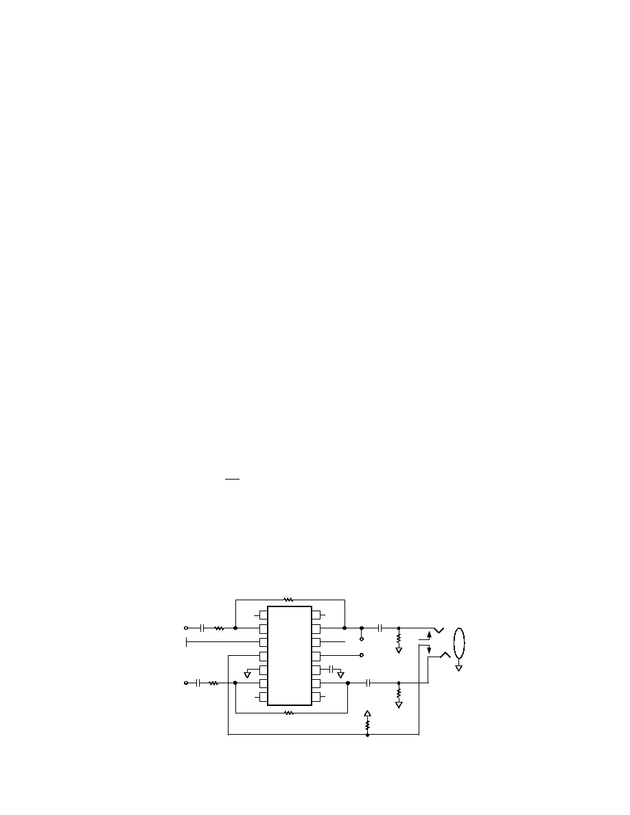
Figure 1. Functional Block Diagram
SoundMax is a registered trademark of Analog Devices, Inc.
14-Lead TSSOP
(RU Suffix)
NC
LEFT IN
SHUTDOWN
GND
RIGHT IN
NC
LEFT OUT/BTL
V
DD
BTL
NC
RIGHT OUT
NC
BYPASS
1
14
7
8
SSM2250
NC = NO CONNECT
SE/BTL
2
REV. 0
SSM2250SPECIFICATIONS
ELECTRICAL CHARACTERISTICS
Parameter
Symbol
Conditions
Min
Typ
Max
Unit
DEVICE CHARACTERISTICS
Output Offset Voltage
V
OS
BTL Mode; A
V
= 2; BTL+ to BTL
4
100
mV
Large Signal Voltage Gain
A
VO
R
L
= 2 k
2
V/mV
Output Power
P
OUT
SE Mode: R
L
= 32
, THD < 1%
90
mW
BTL Mode: R
L
= 8
, THD < 1%
1,000
mW
Output Impedance
Z
OUT
0.1
SHUTDOWN INPUT
Input Voltage High
V
IH
I
S
< 100
µ
A
2.0
V
Input Voltage Low
V
IL
I
S
> 1 mA
0.8
V
POWER SUPPLY
Supply Current
I
S
BTL Mode
6.4
mA
SE Mode
6.4
mA
Supply Current/Amplifier
I
S
60
µ
A
DYNAMIC PERFORMANCE
Slew Rate
SR
R
L
= 100 k
, C
L
= 50 pF
4
V/
µ
s
Gain Bandwidth Product
GBP
4
MHz
Phase Margin
o
84
Degrees
NOISE PERFORMANCE
Voltage Noise Density
e
n
f = 1 kHz
45
nV/
Hz
Specifications subject to change without notice.
(V
S
= 5.0 V, V
CM
= 2.5 V, T
A
= 25 C unless otherwise noted)
ELECTRICAL CHARACTERISTICS
Parameter
Symbol
Conditions
Min
Typ
Max
Unit
DEVICE CHARACTERISTICS
Output Offset Voltage
V
OS
BTL Mode; A
V
= 2; BTL+ to BTL
4
100
mV
Large Signal Voltage Gain
A
VO
R
L
= 2 k
2
V/mV
Output Power
P
OUT
SE Mode: R
L
= 32
, THD < 1%
25
mW
BTL Mode: R
L
= 8
, THD < 1%
300
mW
Output Impedance
Z
OUT
0.1
SHUTDOWN INPUT
Input Voltage High
V
IH
I
S
< 100
µ
A
2.0
V
Input Voltage Low
V
IL
I
S
> 1 mA
0.8
V
POWER SUPPLY
Supply Current
I
S
BTL Mode
6.4
mA
SE Mode
6.4
mA
Supply Current/Amplifier
I
S
32
µ
A
DYNAMIC PERFORMANCE
Slew Rate
SR
R
L
= 100 k
, C
L
= 50 pF
4
V/
µ
s
Gain Bandwidth Product
GBP
4
MHz
Phase Margin
o
84
Degrees
NOISE PERFORMANCE
Voltage Noise Density
e
n
f = 1 kHz
45
nV/
Hz
Specifications subject to change without notice.
(V
S
= 2.7 V, V
CM
= 1.35 V, T
A
= 25 C unless otherwise noted)
SSM2250
3
REV. 0
ABSOLUTE MAXIMUM RATINGS
1
Supply Voltage . . . . . . . . . . . . . . . . . . . . . . . . . . . . . . . . . . 6 V
Differential Input Voltage
2
. . . . . . . . . . . . . . . . . . . . . . . .
±
5 V
Common-Mode Input Voltage . . . . . . . . . . . . . . . . . . . .
±
6 V
ESD Susceptibility . . . . . . . . . . . . . . . . . . . . . . . . . . . . 2000 V
Storage Temperature Range
RM, RU Packages . . . . . . . . . . . . . . . . . . 65
°
C to +150
°
C
Operating Temperature Range
SSM2250 . . . . . . . . . . . . . . . . . . . . . . . . . . 40
°
C to +85
°
C
Junction Temperature Range
RM, RU Packages . . . . . . . . . . . . . . . . . . 65
°
C to +165
°
C
Lead Temperature Range (Soldering, 60 sec) . . . . . . . . 300
°
C
NOTES
1
Stresses above those listed under Absolute Maximum Ratings may cause perma-
nent damage to the device. This is a stress rating only; functional operation of the
device at these or any other conditions above those listed in the operational sections
of this specification is not implied. Exposure to absolute maximum rating condi-
tions for extended periods may affect device reliability.
2
Differential Input Voltage or
±
V
S
, whichever is lower.
Package Type
JA
1
JC
Unit
10-Lead MSOP (RM)
200
44
°
C/W
14-Lead TSSOP (RU)
180
35
°
C/W
NOTE
1
JA
is specified for worst-case conditions, i.e.,
JA
is specified for device soldered
in circuit board for surface mount packages.
CAUTION
ESD (electrostatic discharge) sensitive device. Electrostatic charges as high as 4000 V readily
accumulate on the human body and test equipment and can discharge without detection.
Although the SSM2250 features proprietary ESD protection circuitry, permanent damage may
occur on devices subjected to high energy electrostatic discharges. Therefore, proper ESD
precautions are recommended to avoid performance degradation or loss of functionality.
WARNING!
ESD SENSITIVE DEVICE
ORDERING GUIDE
Temperature
Package
Package
Model
Range
Description
Option
SSM2250RM
40
°
C to +85
°
C
10-Lead MSOP
RM-10
SSM2250RU
40
°
C to +85
°
C
14-Lead TSSOP RU-14
SSM2250
4
REV. 0
FREQUENCY Hz
10
0.1
TOTAL HARMONIC DISTORTION %
1
20
20k
100
1k
10k
V
S
= 5V
BTL MODE
R
L
= 8
C
B
= 1 F
P
OUT
= 1W
A
V
= 2
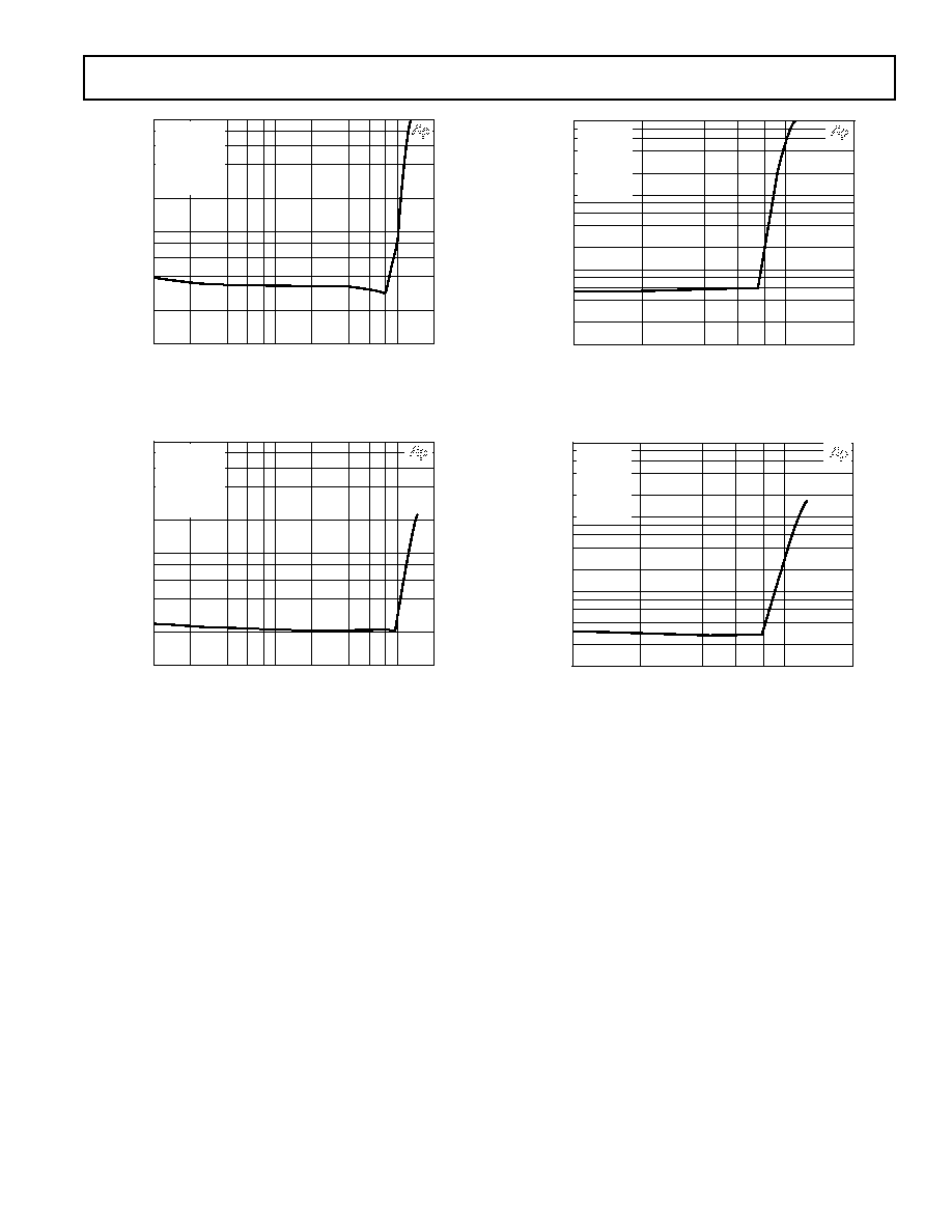
Figure 2. BTL Out THD + N vs. Frequency
20
20k
100
1k
10k
FREQUENCY Hz
10
0.1
TOTAL HARMONIC DISTORTION %
1
V
S
= 2.7V
BTL MODE
R
L
= 8
C
B
= 1 F
P
OUT
= 0.25W
A
V
= 2
Figure 3. BTL Out THD + N vs. Frequency
OUTPUT POWER W
10
1
0.1
10m
2
100m
TOTAL HARMONIC DISTORTION
%
1
V
S
= VARIES
BTL MODE
R
L
= 8
C
B
= 1 F
V
IN
= 1kHz
A
V
= 2
2.7V
3.3V
5V
Figure 4. THD + N vs. Output Power
FREQUENCY Hz
1
0.01
20
20k
100
TOTAL HARMONIC DISTORTION %
1k
0.1
10k
V
S
= 5V
SE MODE
R
L
= 32
C
B
= 1 F
P
OUT
= 60mW
A
V
= 1
Figure 5. SE Out THD + N vs. Frequency
FREQUENCY Hz
1
0.01
20
20k
100
TOTAL HARMONIC DISTORTION %
1k
0.1
10k
V
S
= 2.7V
SE MODE
R
L
= 32
C
B
= 1 F
P
OUT
= 15mW
A
V
= 1
Figure 6. SE Out THD + N vs. Frequency
OUTPUT POWER mW
10
1
0.01
10
200
100
TOTAL HARMONIC DISTORTION %
0.1
5V
3.3V
SE MODE
R
L
= 32
C
B
= 1 F
V
IN
= 1kHz
2.7V
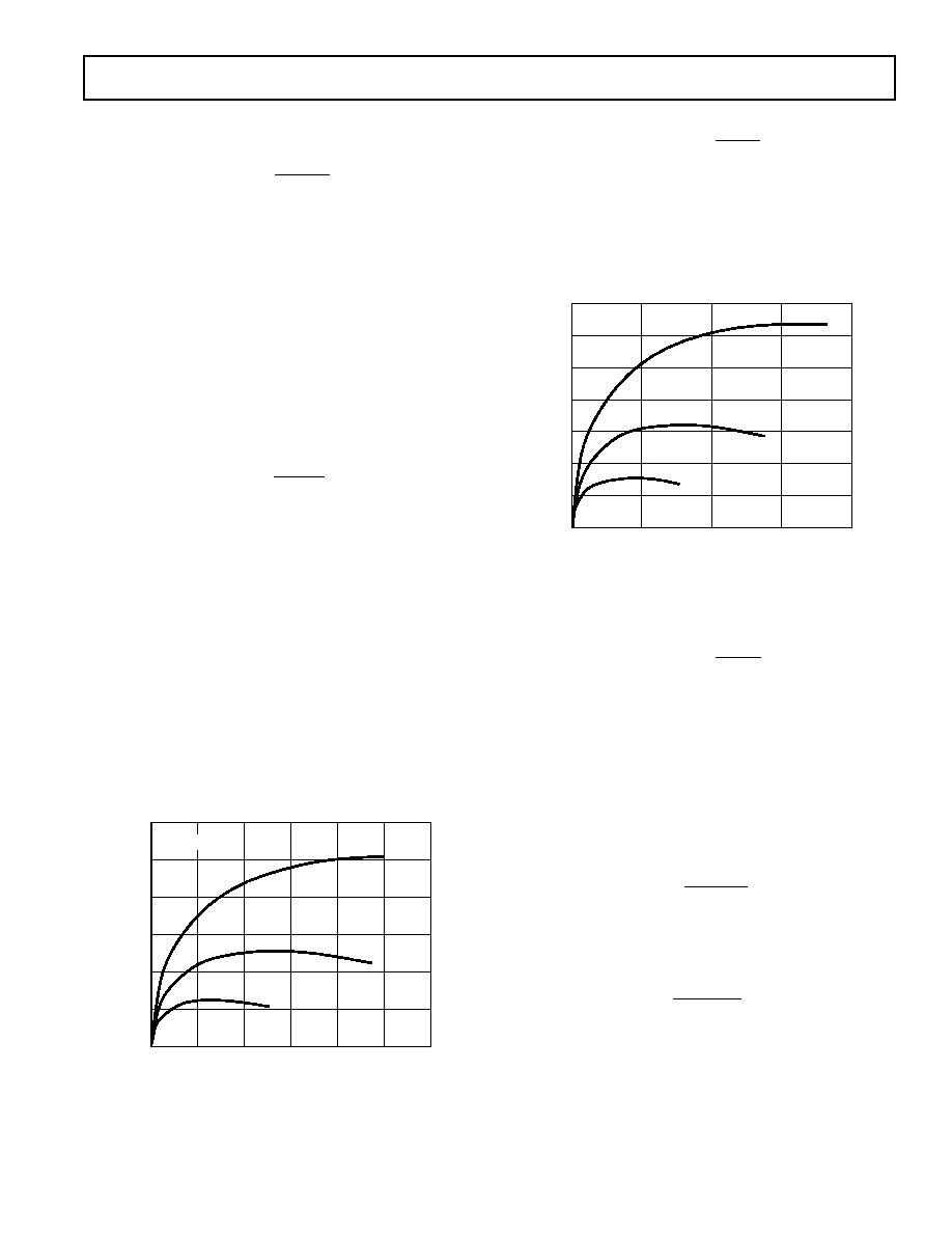
Figure 7. BTL Out THD + N vs. Output Power
SSM2250
5
REV. 0
OUTPUT POWER W
10
1
0.1
10m
2
100m
TOTAL HARMONIC DISTORTION
%
1
V
S
= 5V
BTL MODE
R
L
= 8
C
B
= 1 F
V
IN
= 20Hz
A
V
= 2
Figure 8. BTL Out THD + N vs. Output Power at 20 Hz
OUTPUT POWER W
10
1
0.1
10m
2
100m
TOTAL HARMONIC DISTORTION
%
1
V
S
= 5V
BTL MODE
R
L
= 8
C
B
= 1 F
V
IN
= 20kHz
A
V
= 2
Figure 9. BTL Out THD + N vs. Output Power at 20 kHz
OUTPUT POWER mW
10
1
0.01
10
200
100
TOTAL HARMONIC DISTORTION %
0.1
V
S
= 5V
SE MODE
R
L
= 32
C
B
= 1 F
V
IN
= 20Hz
A
V
= 1
Figure 10. SE Out THD + N vs. Output Power at 20 Hz
OUTPUT POWER mW
10
1
0.01
10
200
100
TOTAL HARMONIC DISTORTION %
0.1
V
S
= 5V
SE MODE
R
L
= 8
C
B
= 1 F
V
IN
= 20kHz
A
V
= 1
Figure 11. SE Out THD + N vs. Output Power at 20 kHz
SSM2250
6
REV. 0
PRODUCT OVERVIEW
The SSM2250 is a low distortion power amplifier that can drive a
set of stereo headphones or a single 8
loudspeaker. It contains
three rail-to-rail output op amps, click and pop reduction biasing,
and all necessary switching circuitry. In SE (Single-Ended) Mode,
the device automatically mutes the internal 8
speaker. In BTL
(Bridge-Tied Load) Mode, the internal speaker is activated.
The SSM2250 can operate from a 2.7 V to 5.5 V single supply.
The rail-to-rail outputs can be driven to within 400 mV of either
supply rail while supplying a sustained output current of 350 mA
into 8
. The device is unity-gain stable and requires no exter-
nal compensation capacitors. The SSM2250 can be configured
for gains of up to 40 dB.
TYPICAL APPLICATION
In SE Mode, the device operates similar to a high current output,
dual op amp. A1 and A3 are independent amplifiers with a gain of
R2/R1. The outputs of A1 and A3 are used to drive the external
headphones plugged into the headphone jack. Amplifier A2 is shut
down to a high output impedance state. This prevents current from
flowing through the 8
internal speaker, thereby muting it.
Although the gains of A1 and A3 can be set independently, it is
recommended that the feedback and feedforward resistor around
both amplifiers be equal. This will prevent one channel from
becoming louder than the other.
In BTL mode, the current into the Right In pin is directed to
the input of A1. This effectively sums the Left and Right In
audio signals. The A2 amplifier is activated and configured with
a fixed gain of A
V
= 1. This produces a balanced output con-
figuration that drives the internal speaker. Because the BTL
output voltages swing opposite to each other, the gain to the
speaker in BTL mode is twice the gain of SE mode. The voltage
across the internal speaker can be written:
V
V
V
R
R
SPEAKER
LEFT
RIGHT
=
+
(
)
× ×
2
2
1
(1)
The bridged output configuration offers the advantage of a more
efficient power transfer from the input to the speaker. Because
both outputs are symmetric, the dc voltage bias across the 8
internal speaker is zero. This eliminates the need for a coupling
capacitor at the output. In BTL mode, the A3 amplifier is shut
down to conserve power.
In BTL Mode, the SSM2250 can achieve 1 W continuous output
into 8
at ambient temperatures up to 40
°
C. The power derating
curve shown in Figure 15 should be observed for proper operation at
higher ambient temperatures. For a standard 14-lead TSSOP pack-
age, typical junction-to-ambient temperature thermal resistance (
JA
)
is 180
°
C/W on a 2-layer board, and 140
°
C/W on a 4-layer board.
Internal Speaker/External Headphones Automatic Switching
Pin 4 on the SSM2250 controls the switching between BTL and
SE Modes. Logic low to Pin 4 activates BTL Mode, while logic
high activates SE Mode. The configuration shown in Figure 12
provides the appropriate logic voltages to Pin 4, muting the
internal speaker when headphones are plugged into the jack.
A stereo headphone jack with a normalizing pin is required for
the application. With no plug inserted, a mechanical spring
connects the normalizing pin to the output pin in the jack.
Once a plug is inserted, this connection is broken.
Referring to Figure 12, Pin 4 of the SSM2250 is connected to the
normalizing pin for the right channel output. This is the pin in
the headphone jack that will hit the ring on the headphone plug.
A 100 k
pull-up resistor to 5 V is also connected at this point.
With a headphone plug inserted, the normalizing pin disconnects
from the output pin, and Pin 4 is pulled up to 5 V, activating SE
Mode on the SSM2250. This mutes the internal speaker while
driving the stereo headphones.
Once the headphone plug is removed, the normalizing pin con-
nects to the output pin. This drives the voltage at Pin 4 to 50 mV,
as this point is pulled low by the 1 k
resistor now connected to
the node. The SSM2250 goes into BTL mode, deactivating the
right SE amplifier to prevent the occurrence of any false mode
switching.
It is important to connect Pin 4 and the 100 k
pull up resistor
to the normalizing pin for the right output in the headphone
jack. Connecting them to the left output normalizing pin will
result in improper operation from the device. The normalizing
pin to the left output in the headphone jack should be left open.
Coupling Capacitors
Output coupling capacitors are not required to drive the internal
speaker from the BTL outputs. However, coupling capacitors are
required between the amplifier's SE outputs and the headphone
jack to drive external headphones. This prevents dc current from
flowing through the headphone speakers, whose resistances are
typically on the order of 80
.
LEFT IN
1 F
NC
NC
R2
20k
SHUTDOWN
10 F
NC
NC
+
BTL
OUT
5V
220 F
+
1k
NC
1k
RIGHT IN
100k
5V
220 F
+
R1
20k
1
2
3
4
5
6
7
14
13
12
11
10
9
8
R1
20k
1 F
R2
20k
NC = NO CONNECT
SSM2250
Figure 12. Typical Application
SSM2250
7
REV. 0
The output coupling capacitor creates a high-pass filter with a
cutoff frequency of:
f
R C
dB
L
C
-
=
3
1
2
(2)
Where, R
L
is the resistance of the headphone, and
C
C
is the output coupling capacitor.
Although a majority of headphones have around 80
of resistance,
this resistance can vary between models and manufacturers. Head-
phone resistances are commonly between 32
to 600
. Using a
220
µ
F capacitor as shown in Figure 12, the worst-case 3 dB corner
frequency would be 22 Hz, with a 32
headphone load. Smaller
output capacitors could be used at the expense of low frequency
response to the headphones.
An input coupling capacitor should be used to remove dc bias
from the inputs to the SSM2250. Again, the input coupling
capacitor in combination with the input resistor will create a
high-pass filter with a corner frequency of:
f
R C
dB
-
=
3
1
2
1 1
(3)
Using the values shown in Figure 2, where R1 = 20 k
and
C1 = 1
µ
F, will create a corner frequency of 8 Hz. This is
acceptable, as the PC 99 audio requirement specifies the com-
puter audio system bandwidth to be 20 Hz to 20 kHz.
Pin 10 on the SSM2250 provides the proper bias voltage for the
amplifiers. A 0.1
µ
F capacitor should be connected here to
reduce sensitivity to noise on the power supply. A larger capaci-
tor can be used should more rejection from power supply noise
be required.
The SSM2250 has excellent phase margin and is stable even
under heavy loading. Therefore, a feedback capacitor in parallel
with R2 is not required, as it is in some competitors' products.
Power Dissipation
An important advantage in using a bridged output configuration
is the fact that bridged output amplifiers are more efficient than
single-ended amplifiers in delivering power to a load.
OUTPUT POWER W
1.5
0
0
0.25
POWER DISSIPATION W
1.25
1.0
0.75
0.5
0.25
0.5
0.75
1.0
1.25
1.5
R
L
= 4
R
L
= 8
R
L
= 16
V
DD
= 5V
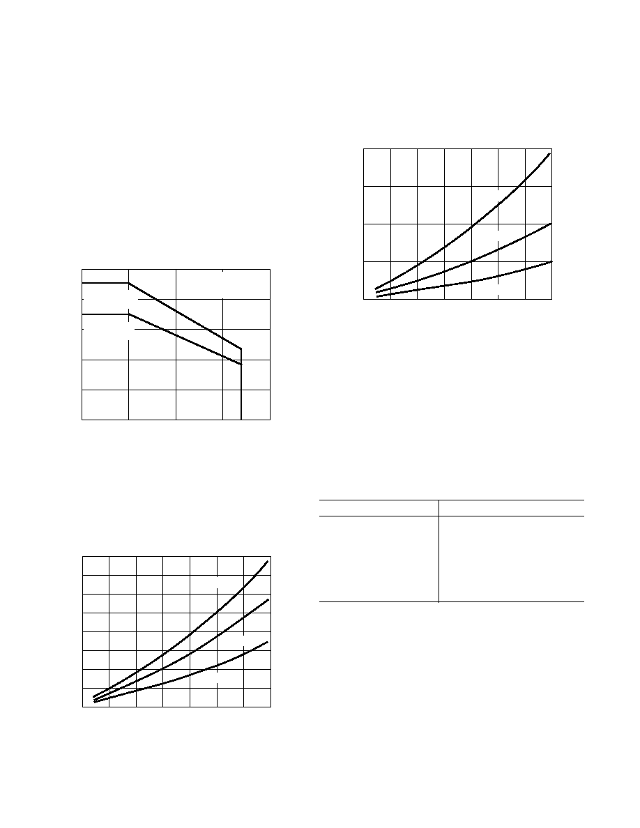
Figure 13. Power Dissipation vs. Output Power in BTL Mode
P
V
R
DISS MAX
DD
L
,
=
2
2
2
(4)
Using Equation 4 and the power derating curve in Figure 15,
the maximum ambient temperature can be easily found. This
ensures that the SSM2250 will not exceed its maximum junc-
tion temperature of 150
°
C.
The power dissipation for a single-ended output application where
an output coupling capacitor is used is shown in Figure 14.
OUTPUT POWER W
0.35
0.3
0
0
0.4
0.1
POWER DISSIPATION W
0.2
0.3
0.2
0.15
0.1
0.05
0.25
R
L
= 4
R
L
= 8
R
L
= 16
V
DD
= 5V
Figure 14. Power Dissipation vs. Single-Ended Output
Power (V
DD
= 5 V)
The maximum power dissipation for a single-ended output is:
P
V
R
DISS MAX
DD
L
,
=
2
2
2
(5)
Because the SSM2250 is designed to drive two single-ended
loads simultaneously, the worst-case maximum power dissipation
in SE Mode is twice the value of Equation 5.
A thorough mathematical explanation behind Equation 4 and
Equation 5 is given in the SSM2211 data sheet, which can be
downloaded at http://www.analog.com.
Example: Given worst-case stereo headphone loads of 32
,
the maximum power dissipation of the SSM2250 in SE Mode
with a 5 V supply would be:
P
V
mW
DISS
MAX
,
=
( )
=
5
2
32
79
2
2
(6)
With an 8
internal speaker attached, the maximum power
dissipation in BTL mode is (from Equation 4):
P
V
mW
DISS
MAX
,
=
×
( )
=
2
5
8
633
2
2
(7)
It can be easily seen that power dissipation from BTL Mode
operation is of greater concern than SE Mode.
Solving for Maximum Ambient Temperature
To protect the SSM2250 against thermal damage, the junction
temperature of the die should not exceed 150
°
C. The maximum
allowable ambient temperature of the application can be easily
found by solving for the expected maximum power dissipation in
Equation 4 and Equation 5, and using Equation 8.
SSM2250
8
REV. 0
Continuing from the previous example, the
JA
of the SSM2250
14-lead TSSOP package on a 4-layer board is 140
°
C/W. To ensure
the SSM2250 die junction temperature stays below 150
°
C, the
maximum ambient temperature can be solved using Equation 8.
T
150 C
P
AMB, MAX
JA
DISS, MAX
= +
° -
×
= +
° -
°
×
(
)
150
140
0 633
C
C/W
W
.
(8)
= + °
61 C
So the maximum ambient temperature must remain below 61
°
C
to protect the device against thermal damage.
Another method for finding the maximum allowable ambient
temperature is to use the power derating curve in Figure 15.
The y-axis corresponds to the expected maximum power dissi-
pation, and the x-axis is the corresponding maximum ambient
temperature. Either method will return the same answer.
AMBIENT TEMPERATURE C
1.0
0.8
0
0
100
25
POWER DISSIPATION W
50
75
0.6
0.4
0.2
14-LEAD TSSOP
JA
= 140 C/W
10-LEAD MSOP
JA
= 180 C/W
T
J,MAX
= 150 C/W
FREE AIR
NO HEAT SINK
Figure 15. Maximum Power Dissipation vs. Ambient
Temperature
Maximum Output Power
The maximum amount of power that can be delivered to a
speaker is a function of the supply voltage and the resistance of
the speaker. Figure 15 shows the maximum BTL output power
possible from the SSM2250. Maximum output power is defined
as the point at which the output has greater than 1% distortion.
SUPPLY VOLTAGE V
1.5
5.0
2.0
2.5
3.0
3.5
4.0
4.5
1.6
0
MAXIMUM OUTPUT @ THD 1% W
1.4
0.8
0.6
0.4
0.2
1.2
1.0
R
L
= 4
R
L
= 8
R
L
= 16
Figure 16. Maximum BTL Output Power vs. V
S
To find the minimum supply voltage needed to achieve a speci-
fied maximum undistorted output power, simply use Figure 16.
The output power in SE mode is exactly one-fourth the equivalent
output power in BTL mode. This is because twice the voltage swing
across the two BTL outputs results in 4 the power delivered to the
load. Figure 17 shows the maximum output power in SE mode vs.
supply voltage for various headphone loads.
SUPPLY VOLTAGE V
1.5
5.0
2.0
2.5
3.0
3.5
4.0
4.5
100
0
MAXIMUM OUTPUT @ THD 1% mW
50
25
75
R
L
= 32
R
L
= 64
R
L
= 128
Figure 17. Maximum SE Output Power vs. V
S
Example: An application requires only 500 mW to be output in
BTL Mode into an 8
speaker. By inspection, the minimum
supply voltage required is 3.3 V.
Speaker Efficiency and Loudness
The effective loudness of 1 W of power delivered into an 8
speaker is a function of the efficiency of the speaker. The efficiency
of a speaker is typically rated at the sound pressure level (SPL) at
1 meter in front of the speaker with 1 W of power applied to the
speaker. Most speakers are between 85 dB and 95 dB SPL at one
meter at 1 W of power. Table I shows a comparison of the relative
loudness of different sounds.
Table I. Typical Sound Pressure Levels
Source of Sound
dB SPL
Threshold of Pain
120
Heavy Street Traffic
95
Cabin of Jet Aircraft
80
Average Conversation
65
Average Home at Night
50
Quiet Recording Studio
30
Threshold of Hearing
0
It can be easily seen that 1 W of power into a speaker can produce
quite a bit of acoustic energy.
Shutdown Feature
The SSM2250 can be put into a low power consumption shut-
down mode by connecting Pin 3 to V
DD
. In shutdown mode, the
SSM2250 has low supply current of 60
µ
A.
Pin 3 should be connected to ground for normal operation. Con-
necting Pin 3 to V
DD
will shut down all amplifiers and put all outputs
into a high impedance state, effectively muting the SSM2250. A
pull-up or pull-down resistor is not required. Pin 3 should never be
left floating as this could produce unpredictable results.
PC 99 Compliant Computer Audio Reference Design
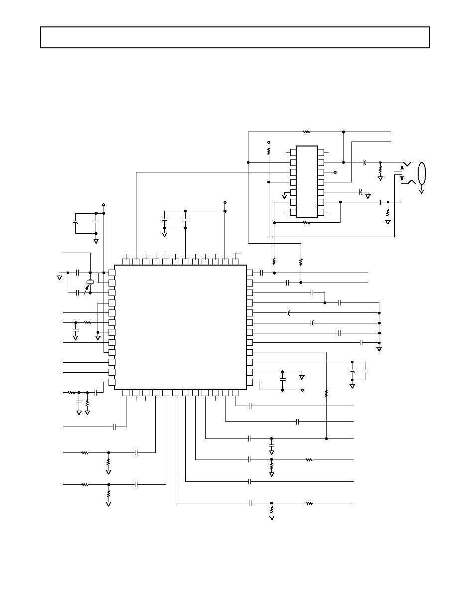
The schematic shown in Figure 18 is a reference design for a
complete audio system in a computer. The design is compliant
with the PC 99 standard for computer audio.
SSM2250
9
REV. 0
C7
0.1 F
C6
10 F
36
35
34
33
32
31
30
29
28
27
26
25
1
2
3
4
5
6
7
8
9
10
11
12
SSM2250
C4
10 F
+
1
2
3
4
5
6
7
NC
NC
R1
20k
NC
NC
AV
DD
= 5V
R3
1k
NC
R4
1k
R5
20k
C1
100 F
+
TO SPEAKER
TO SPEAKER+
C5
100 F
+
R2
100k
AV
DD
= 5V
48
47
46
45
44
43
42
41
40
39
38
37
13
14
15
16
17
18
19
20
21
22
23
24
14
13
12
11
10
9
8
C24
1 F
LINE IN RIGHT
C25
1 F
C27
1 F
C28
0.001 F
C30
1 F
R15
4.7k
R13
4.7k
C32
1 F
C33
1 F
R19
4.7k
R18
4.7k
NC
C31
1 F
R17
4.7k
R16
4.7k
AUX IN
MONO
PHONE
C29
1 F
R14
4.7k
R12
4.7k
C26
1 F
AUX
LEFT
PCBEEP
C22
1 F
C23
0.1 F
C9
1 F
C10
1 F
C13
0.047 F
C15
1 F
C16
270pF
C17
270pF
C12
0.1 F
C14
1 F
LINE OUT RIGHT
LINE OUT LEFT
AV
DD
= 5V
C21
0.1 F
C16
10 F
C19
0.1 F
R9
2k
R10
10k
R11
1k
RST#
SYNC
SDATA
IN 0
BITCLK
SDATA
OUT
C20
27pF
R8
47
Y1
24.576MHz
SMT
AC CLK
C11
22pF
C8
22pF
AV
DD
= 5V
NC
MONO OUT
AV
DD
= 5V
C3
0.1 F
C2
10 F
AD1881
LINE IN LEFT
MIC IN
CD GND
CD RIGHT
CD LEFT
R6
20k
R7
20k
NC = NO CONNECT
NC NC NC NC
NC NC NC
NC
NC
Figure 18. PC 99 Compliant Audio System Reference Design
The AD1881 is an AC'97 Ver. 2.1 audio codec available from
Analog Devices. The stereo output from the AD1881 is coupled
into the SSM2250, which is used to drive a mono internal
speaker and stereo headphones. The internal speaker switching
is controlled by the SSM2250 through the normalizing pin on
the headphone jack. The AD1881 controls the shutdown pin on
the SSM2250, and is activated through the power management
software drivers installed on the computer.
For more information on the AD1881, the data sheet
can be downloaded from the Analog Devices web site at
http://www.analog.com.
SSM2250
10
REV. 0
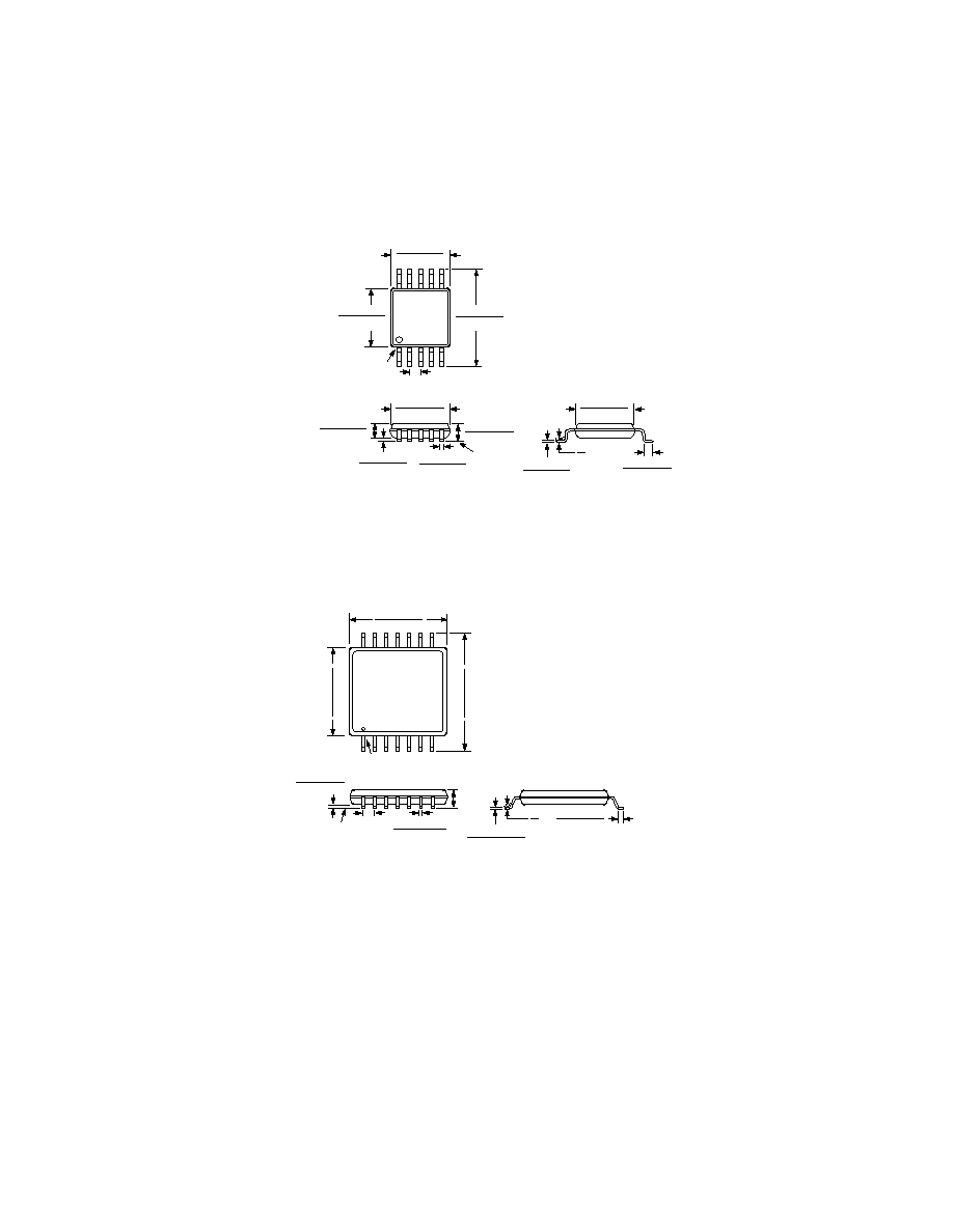
OUTLINE DIMENSIONS
Dimensions shown in inches and (mm).
10-Lead MSOP
(RM Suffix)
0.199 (5.05)
0.187 (4.75)
1
10
6
5
PIN 1
0.0197 (0.50) BSC
0.124 (3.15)
0.112 (2.84)
0.124 (3.15)
0.112 (2.84)
0.122 (3.10)
0.110 (2.79)
SEATING
PLANE
0.006 (0.15)
0.002 (0.05)
0.016 (0.41)
0.006 (0.15)
0.038 (0.97)
0.030 (0.76)
0.043 (1.09)
0.037 (0.94)
0.011 (0.28)
0.003 (0.08)
0.022 (0.56)
0.021 (0.53)
0.120 (3.05)
0.112 (2.84)
6
0
14-Lead TSSOP
(RU Suffix)
14
8
7
1
0.201 (5.10)
0.193 (4.90)
0.256 (6.50)
0.246 (6.25)
0.177 (4.50)
0.169 (4.30)
PIN 1
SEATING
PLANE
0.006 (0.15)
0.002 (0.05)
0.0118 (0.30)
0.0075 (0.19)
0.0256
(0.65)
BSC
0.0433
(1.10)
MAX
0.0079 (0.20)
0.0035 (0.090)
0.028 (0.70)
0.020 (0.50)
8
0
C37292.510/99
PRINTED IN U.S.A.