 | ÐлекÑÑоннÑй компоненÑ: SSM2302 | СкаÑаÑÑ:  PDF PDF  ZIP ZIP |
Äîêóìåíòàöèÿ è îïèñàíèÿ www.docs.chipfind.ru
Filterless High Efficiency
Class-D Stereo Audio Amplifier
SSM2302
Rev. 0
Information furnished by Analog Devices is believed to be accurate and reliable. However, no
responsibility is assumed by Analog Devices for its use, nor for any infringements of patents or other
rights of third parties that may result from its use. Specifications subject to change without notice. No
license is granted by implication or otherwise under any patent or patent rights of Analog Devices.
Trademarks and registered trademarks are the property of their respective owners.
One Technology Way, P.O. Box 9106, Norwood, MA 02062-9106, U.S.A.
Tel: 781.329.4700
www.analog.com
Fax: 781.461.3113
©2006 Analog Devices, Inc. All rights reserved.
FEATURES
Filterless Class-D amplifier with built-in output stage
1.4 W into 8 at 5.0 V supply with less than 1% THD
85% efficiency at 5.0 V, 1.4 W into 8 speaker
Better than 98 dB SNR (signal-to-noise ratio)
Single-supply operation from 2.5 V to 5.0 V
20 nA ultralow shutdown current
Short-circuit and thermal protection
Available in 16-lead, 3 mm × 3 mm LFCSP
Pop-and-click suppression
Built-in resistors reduce board component count
Fixed and user-adjustable gain configurations
APPLICATIONS
Mobile phones
MP3 players
Portable gaming
Portable electronics
Educational toys
GENERAL DESCRIPTION
The SSM2302 is a fully integrated, high efficiency, Class-D stereo
audio amplifier. It is designed to maximize performance for
mobile phone applications. The application circuit requires a
minimum of external components and operates from a single
2.5 V to 5.0 V supply. It is capable of delivering 1.4 W of con-
tinuous output power with less than 1% THD + N driving an
8 load from a 5.0 V supply.
The SSM2302 features a high efficiency, low noise modulation
scheme. It operates with 85% efficiency at 1.4 W into 8 from a
5.0 V supply and has a signal-to-noise ratio (SNR) that is better
than 98 dB. PDM modulation is used to provide lower EMI-
radiated emissions compared with other Class-D architectures.
The SSM2302 has a micropower shutdown mode with a typical
shutdown current of 20 nA. Shutdown is enabled by applying a
logic low to the SD pin.
The architecture of the device allows it to achieve a very low level
of pop and click. This minimizes voltage glitches at the output
during turn-on and turn-off, thus reducing audible noise on
activation and deactivation.
The fully differential input of the SSM2302 provides excellent
rejection of common-mode noise on the input. Input coupling
capacitors can be omitted if the dc input common-mode voltage
is approximately V
DD
/2.
The SSM2302 also has excellent rejection of power supply noise,
including noise caused by GSM transmission bursts and RF
rectification. PSRR is typically 63 dB at 217 Hz.
The gain can be set to 6 dB or 12 dB utilizing the gain control
select pin connected respectively to ground or V
DD
. Gain can
also be adjusted externally by using an external resistor.
The SSM2302 is specified over the commercial temperature range
(-40°C to +85°C). It has built-in thermal shutdown and output
short-circuit protection. It is available in a 16-lead, 3 mm × 3 mm
lead-frame chip scale package (LFCSP).
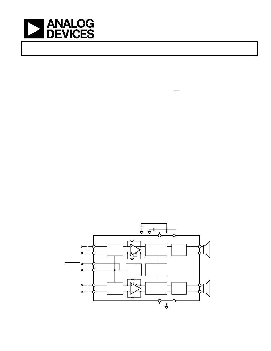
FUNCTIONAL BLOCK DIAGRAM
GAIN
CONTROL
FET
DRIVER
MODULATOR
0.1µF
VDD
VDD
GND
GND
INTERNAL
OSCILLATOR
OUTR+
OUTR
OUTL+
OUTL
GAIN
CONTROL
BIAS
FET
DRIVER
MODULATOR
INR+
VBATT
2.5V TO 5.0V
INR
GAIN
SD
GAIN
SHUTDOWN
INL+
INL
10µF
0.01µF
1
1
INPUT CAPS ARE OPTIONAL IF INPUT DC COMMON-MODE
VOLTAGE IS APPROXIMATELY V
DD
/2.
0.01µF
1
0.01µF
1
0.01µF
1
LEFT IN+
LEFT IN
RIGHT IN
RIGHT IN+
SSM2302
06
05
1-
0
01
Figure 1.

SSM2302
Rev. 0 | Page 2 of 20
TABLE OF CONTENTS
Features .............................................................................................. 1
Applications....................................................................................... 1
General Description ......................................................................... 1
Functional Block Diagram .............................................................. 1
Revision History ............................................................................... 2
Specifications..................................................................................... 3
Absolute Maximum Ratings............................................................ 4
Thermal Resistance ...................................................................... 4
ESD Caution.................................................................................. 4
Pin Configuration and Function Descriptions............................. 5
Typical Performance Characteristics ............................................. 6
Typical Application Circuits............................................................ 9
Application Notes ........................................................................... 12
Overview...................................................................................... 12
Gain Selection ............................................................................. 12
Pop-and-Click Suppression ...................................................... 12
EMI Noise.................................................................................... 12
Layout .......................................................................................... 13
Input Capacitor Selection.......................................................... 13
Proper Power Supply Decoupling ............................................ 13
Evaluation Board Information...................................................... 14
Introduction ................................................................................ 14
Operation .................................................................................... 14
SSM2302 Application Board Schematic.................................. 15
SSM2302 Stereo Class-D Amplifier Evaluation Module
Component List.......................................................................... 16
SSM2302 Application Board Layout........................................ 17
Outline Dimensions ....................................................................... 18
Ordering Guide .......................................................................... 18
REVISION HISTORY
6/06--Revision 0: Initial Version
SSM2302
Rev. 0 | Page 3 of 20
SPECIFICATIONS
V
DD
= 5.0 V, T
A
= 25
o
C, R
L
= 8 , unless otherwise noted
Table 1.
Parameter Symbol
Conditions
Min
Typ
Max
Unit
DEVICE CHARACTERISTICS
Output Power
P
O
R
L
= 8 , THD = 1%, f = 1 kHz, 20 kHz BW, V
DD
= 5.0 V
1.4
W
R
L
= 8 , THD = 1%, f = 1 kHz, 20 kHz BW, V
DD
= 3.6 V
0.615
W
R
L
= 8 , THD = 1%, f = 1 kHz, 20 kHz BW, V
DD
= 2.5 V
0.275
W
R
L
= 8 , THD = 10%, f = 1 kHz, 20 kHz BW, V
DD
= 5.0 V
1.53
W
R
L
= 8 , THD = 10%, f = 1 kHz, 20 kHz BW, V
DD
= 3.6 V
0.77
W
R
L
= 8 , THD = 10%, f = 1 kHz, 20 kHz BW, V
DD
= 2.5 V
0.35
W
Efficiency
P
OUT
=1.4 W, 8 , V
DD
= 5.0 V
85
%
Total Harmonic Distortion + Noise
THD + N
P
O
= 1 W into 8 each channel, f = 1 kHz, V
DD
= 5.0 V
0.1
%
P
O
= 0.5 W into 8 each channel, f = 1 kHz, V
DD
= 3.6 V
0.04
%
Input Common-Mode Voltage Range
V
CM
1.0
V
DD
- 1
V
Common-Mode Rejection Ratio
CMRR
GSM
V
CM
= 2.5 V ± 100 mV at 217 Hz
55
dB
Channel Separation
X
TALK
P
O
= 100 mW
, f = 1 kHz
98
dB
Average Switching Frequency
f
SW
1.8
MHz
Differential Output Offset Voltage
V
OOS
G = 6 dB; G = 12 dB
2.0
mV
POWER SUPPLY
Supply Voltage Range
V
DD
Guaranteed from PSRR test
2.5
5.0
V
Power Supply Rejection Ratio
PSRR
V
DD
= 2.5 V to 5.0 V, 50 Hz, input floating/ground
70
85
dB
PSRR
GSM
V
RIPPLE
= 100 mV at 217 Hz, inputs ac GND,
C
IN
= 0.01 F, input referred
63
dB
Supply Current
I
SY
V
IN
= 0 V, no load, V
DD
= 5.0 V
8.0
mA
V
IN
= 0 V, no load, V
DD
= 3.6 V
6.6
mA
V
IN
= 0 V, no load, V
DD
= 2.5 V
5.3
mA
Shutdown Current
I
SD
SD = GND
20
nA
GAIN CONTROL
Closed-Loop Gain
Av0
GAIN pin = 0 V
6
dB
Av1
GAIN pin = V
DD
12
dB
Differential Input Impedance
Z
IN
SD = VDD,
150
K
SD = GND
210
K
SHUTDOWN CONTROL
Input Voltage High
V
IH
I
SY
1 mA
1.2
V
Input Voltage Low
V
IL
I
SY
300 nA
0.5
V
Turn-On Time
t
WU
SD rising edge from GND to V
DD
30
ms
Turn-Off Time
t
SD
SD falling edge from V
DD
to GND
5
s
Output Impedance
Z
OUT
SD = GND
>100
K
NOISE PERFORMANCE
Output Voltage Noise
e
n
V
DD
= 2.5 V to 5.0 V, f = 20 Hz to 20 kHz, inputs are
ac grounded, sine wave, A
V
= 6 dB, A weighting
35
V
Signal-to-Noise Ratio
SNR
P
OUT
= 1.4 W, R
L
= 8
98
dB
SSM2302
Rev. 0 | Page 4 of 20
ABSOLUTE MAXIMUM RATINGS
Absolute maximum ratings apply at 25°C, unless otherwise noted.
Table 2.
Parameter Rating
Supply Voltage
6 V
Input Voltage
V
DD
Common-Mode Input Voltage
V
DD
Storage Temperature Range
-65°C to +150°C
Operating Temperature Range
-40°C to +85°C
Junction Temperature Range
-65°C to +165°C
Lead Temperature Range
(Soldering, 60 sec)
300°C
Stresses above those listed under Absolute Maximum Ratings
may cause permanent damage to the device. This is a stress
rating only; functional operation of the device at these or any
other conditions above those indicated in the operational
section of this specification is not implied. Exposure to absolute
maximum rating conditions for extended periods may affect
device reliability.
THERMAL RESISTANCE
JA
is specified for the worst-case conditions, that is, a device
soldered in a circuit board for surface-mount packages.
Table 3. Thermal Resistance
Package Type
JA
JC
Unit
16-lead, 3 mm × 3 mm LFCSP
44
31.5
°C/W
ESD CAUTION
ESD (electrostatic discharge) sensitive device. Electrostatic charges as high as 4000 V readily accumulate on
the human body and test equipment and can discharge without detection. Although this product features
proprietary ESD protection circuitry, permanent damage may occur on devices subjected to high energy
electrostatic discharges. Therefore, proper ESD precautions are recommended to avoid performance
degradation or loss of functionality.
SSM2302
Rev. 0 | Page 5 of 20
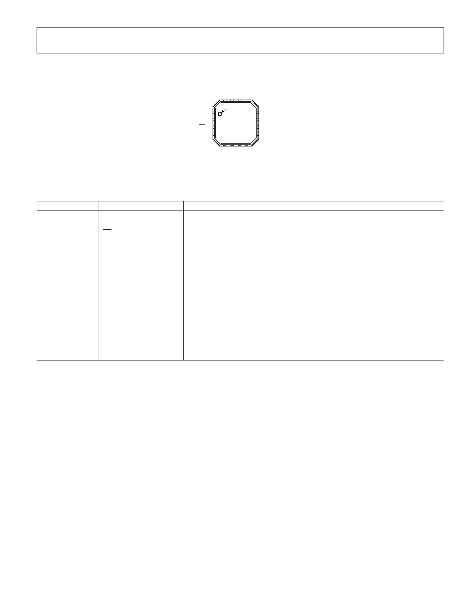
PIN CONFIGURATION AND FUNCTION DESCRIPTIONS
PIN 1
INDICATOR
NC = NO CONNECT
1
OUTL+
2
OUTL
3
SD
4
INL+
11 OUTR
12 OUTR+
10 GAIN
9 INR+
5
I
N
L
6
N
C
7
N
C
8
I
N
R
1
5
V
D
D
1
6
G
N
D
1
4
V
D
D
1
3
G
N
D
TOP VIEW
(Not to Scale)
SSM2302
06
05
1-
0
02
Figure 2. SSM2302 LFCSP Pin Configuration
Table 4. Pin Function Descriptions
Pin No.
Mnemonic
Description
1
OUTL+
Inverting Output for Left Channel.
2
OUTL-
Noninverting Output for Left Channel.
3
SD
Shutdown Input. Active low digital input.
4
INL+
Noninverting Input for Left Channel.
5
INL-
Inverting Input for Left Channel.
6 NC
No
Connect.
7 NC
No
Connect.
8
INR-
Inverting Input for Right Channel.
9
INR+
Noninverting Input for Right Channel.
10
GAIN
Gain Selection. Digital input.
11
OUTR-
Noninverting Output for Right Channel.
12 OUTR+
Inverting Output for Right Channel.
13
GND
Ground for Output Amplifiers.
14
VDD
Power Supply for Output Amplifiers.
15
VDD
Power Supply for Output Amplifiers.
16
GND
Ground for Output Amplifiers.
Document Outline
- þÿ
- þÿ
- þÿ
- þÿ
- þÿ
- þÿ
- þÿ
- þÿ
- þÿ
- þÿ
- þÿ
- þÿ
- þÿ
- þÿ