 | –≠–ª–µ–∫—Ç—Ä–æ–Ω–Ω—ã–π –∫–æ–º–ø–æ–Ω–µ–Ω—Ç: SSM2404P | –°–∫–∞—á–∞—Ç—å:  PDF PDF  ZIP ZIP |
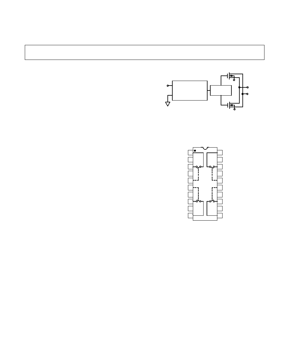
BLOCK DIAGRAM OF ONE SWITCH CHANNEL
CONTROL
DIGITAL
CONTROL
SW1 A
SW1 B
V≠
V+
RAMP
GENERATOR
LOGIC INTERFACE
AND
BREAK-BEFORE-MAKE
CONTROL
PIN CONNECTIONS
Epoxy Mini-DIP (P Suffix)
and SOIC (S Suffix)
SW1 A
SW1 B
DGND
SW1 CONTROL
SW2 CONTROL
NC
*
SW2 B
SW2 A
SW4 A
SW4 B
V+
SW4 CONTROL
SW3 CONTROL
V≠
SW3 B
SW3 A
NC = NO CONNECT
AGND
AGND
AGND
AGND
*
CONNECT TO ANALOG GROUND
FOR BEST NOISE ISOLATION
SW1
1
2
3
4
5
6
7
8
20
19
18
17
16
15
14
13
9
10
12
11
TOP VIEW
(Not to Scale)
O
SSM2404
SW1
SW2
SW3
SW4
REV. B
Information furnished by Analog Devices is believed to be accurate and
reliable. However, no responsibility is assumed by Analog Devices for its
use, nor for any infringements of patents or other rights of third parties
which may result from its use. No license is granted by implication or
otherwise under any patent or patent rights of Analog Devices.
a
Quad Audio Switch
SSM2404
One Technology Way, P.O. Box 9106, Norwood, MA 02062-9106, U.S.A.
Tel: 617/329-4700
Fax: 617/326-8703
FEATURES
"CIickless" Bilateral Audio Switching
Four SPST Switches in a 20-Pin Package
Ultralow THD+N: 0.0008% @ 1 kHz (2 V rms,
R
L
= 100 k )
Low Charge Injection: 35 pC typ
High OFF Isolation: ≠100 dB typ (R
L
= 10 k @ 1 kHz)
Low Crosstalk: ≠94 dB typ (R
L
= 10 k @ 1 kHz)
Low ON Resistance: 28 typ
Low Supply Current: 900 A typ
Single or Dual Supply Operation: +11 V to +24 V or
5.5 V to 12 V
Guaranteed Break-Before-Make
TTL and CMOS Compatible Logic Inputs
Low Cost-Per-Switch
GENERAL DESCRIPTION
The SSM2404 integrates four SPST analog switches in a single
20-pin package. Developed specifically for high performance
audio applications, distortion and noise are negligible over the
full operating range of 20 Hz to 20 kHz. With very low charge
injection of 35 pC, "clickless" audio switching is possible, even
under the most demanding conditions.
Switch control is realized by conventional TTL or CMOS
logic. Guaranteed "break-before-make" operation assures that
all switches in a large system will open before any switch
reaches the ON state.
Single or dual supply operation is possible. Additional features
include ≠100 dB OFF isolation, ≠94 dB crosstalk and 28
ON
resistance. Optional current-mode switching permits an
extended signal-handling range. Although optimized for large
load impedances, the SSM2404 maintains good audio
performance even under low load impedance conditions.
REV. B
≠2≠
SSM2404≠SPECIFICATIONS
(V
S
= 12 V, T
A
= +25 C, unless otherwise noted.
Typical specifications apply at T
A
= +25 C.)
Parameter
Symbol
Conditions
Min
Typ
Max
Units
AUDIO PERFORMANCE
Total Harmonic Distortion Plus Noise
THD+N
@ 1 kHz, with 80 kHz Filter,
R
L
= 100 k
, V
IN
= 2 V rms
0.0008
%
Spectral Noise Density
e
n
20 Hz to 20 kHz
0.8
nV/
Hz
Wideband Noise Density
e
n
p-p
20 Hz to 20 kHz
0.6
µ
V p-p
ANALOG SIGNAL SECTION
Analog Voltage Range
V
A
V
INH
= 2.4 V, I
A
=
±
2 mA
±
12
V
Analog Current Range
I
A
V
INH
= 2.4 V, V
A
= 0 V
±
10
mA
ON Resistance
R
ON
I
A
=
±
10 mA, V
A
=
±
10 V dc
28
45
R
ON
Matching
R
ON
Match
I
A
=
±
10 mA, V
A
= 0 V
1
%
ON Leakage Current
I
S(ON)
V
A
=
±
10 V
≠20
0.1
+20
nA
OFF Leakage Current
I
S(OFF)
V
A
=
±
10 V
≠20
0.1
+20
nA
Charge Injection
Q
35
pC
ON-State Input Capacitance
C
ON
V
A
= 5 V rms
31
pF
OFF-State Input Capacitance
C
OFF
V
A
= 5 V rms
17
pF
OFF Isolation
I
SO(OFF)
V
A
= 50 mV rms, f = 1 kHz, R
L
= 10 k
≠100
dB
Channel-to-Channel Crosstalk
C
T
V
A
= 50 mV rms, f = 1 kHz, R
L
= 10 k
≠94
dB
CONTROL SECTION
Digital Input High
V
INH
DGND = 0 V
2.4
V
S
V
Digital Input Low
V
INL
DGND = 0 V
0
0.8
V
Turn-On Time
1
t
ON
See Test Circuit
8
50
ms
Turn-Off Time
2
t
OFF
See Test Circuit
5
30
ms
Break-Before-Make Time Delay
t
ON
-t
OFF
3
20
ms
Logic Input Current
Logic HI
V
INH
= 2.4 V
≠1000 1.3
+1000
nA
Logic LO
V
INL
= 0.8 V
≠1000 1.0
+1000
nA
POWER SUPPLY
Supply Voltage Range
V
S
Single Supply
+11
+24
V
Dual Supply
±
5.5
±
12
V
Positive Supply Current
I
SY+
All Channels On
0.9
5
mA
Negative Supply Current
I
SY≠
All Channels On
≠1.5
≠0.6
mA
Ground Current
All Channels On
≠2.0
≠0.3
mA
NOTES
1
Turn-on time is measured from the time the logic input reaches the 50% point to the time the output reaches 50% of the final value.
2
Turn-off time is measured from the time the logic input reaches the 50% point to the time the output reaches 50% of the initial value.
Specifications subject to change without notice.
ABSOLUTE MAXIMUM RATINGS
Supply Voltage
Single Supply . . . . . . . . . . . . . . . . . . . . . . . . . . . . . . . +27 V
Dual Supply . . . . . . . . . . . . . . . . . . . . . . . . . . . . . .
±
13.5 V
Analog Input Voltage (V
A
) . . . . . . . . . . . . . . . . . . . . . . . . . . V
S
Logic Input Voltage (V
INL/INH
) . . . . . . . . . . . . . . . . . . . . . . V
S
Maximum Current Through Any Switch . . . . . . . . . . . 20 mA
Operating Temperature Range . . . . . . . . . . . . ≠40
∞
C to +85
∞
C
Storage Temperature Range . . . . . . . . . . . . ≠65
∞
C to +150
∞
C
Junction Temperature (T
J
) . . . . . . . . . . . . . . . . . . . . +150
∞
C
Lead Temperature (Soldering, 60 sec) . . . . . . . . . . . . +300
∞
C
Thermal Resistance
1
20-Pin Plastic DIP (P):
JA
= 74,
JC
= 32 . . . . . . . . .
∞
C/W
20-Pin SOIC (S):
JA
= 90,
JC
= 27 . . . . . . . . . . . . . .
∞
C/W
NOTE
1
JA
is specified for worst case mounting conditions, i.e.,
JA
is specified for device
in socket for P-DIP package.
ORDERING GUIDE
Operating
Temperature
Package
Model
Range
Package
Option*
SSM2404P
≠40
∞
C to +85
∞
C
20-Pin Plastic DIP
N-20
SSM2404S
≠40
∞
C to +85
∞
C
20-Pin SOIC
R-20
*N = Plastic DIP, R = SOIC.
SSM2404
REV. B
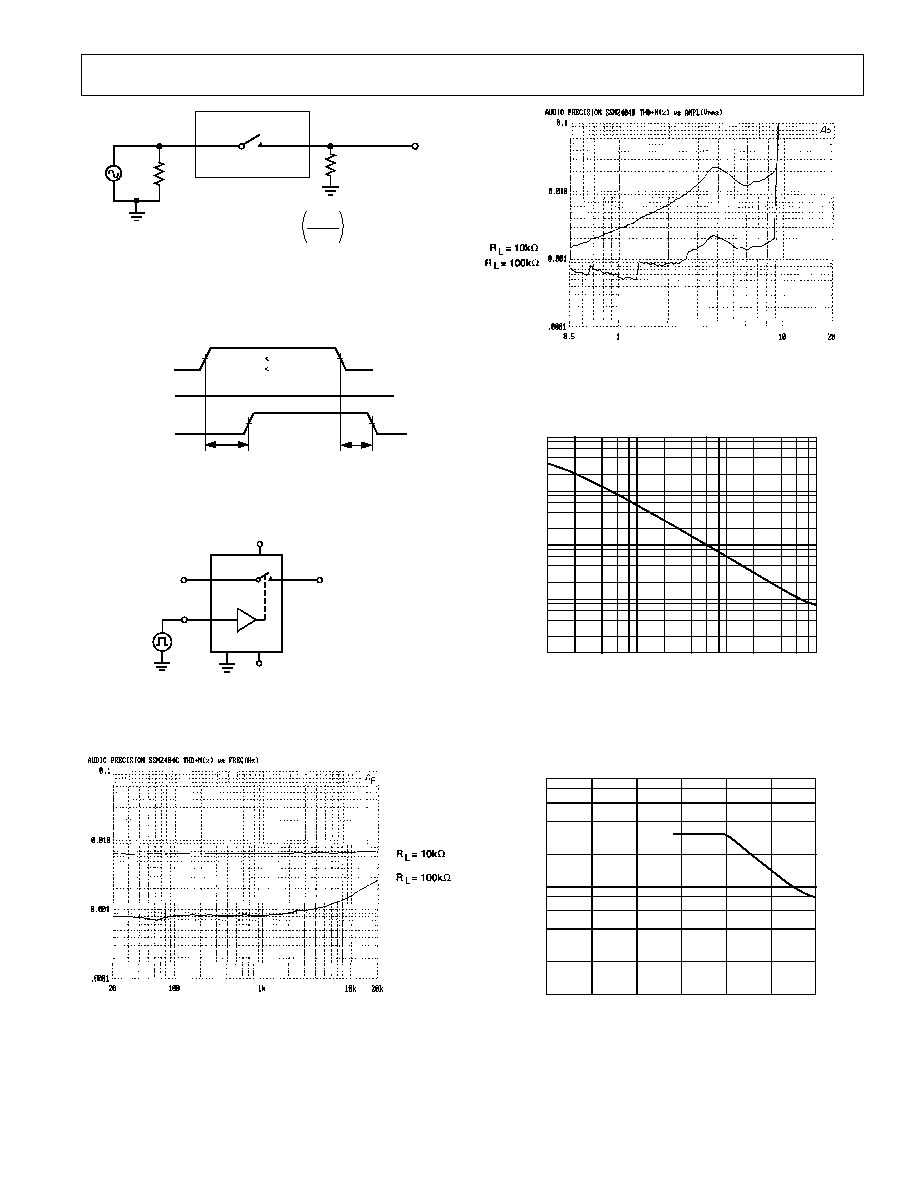
≠3≠
V
A (IN)
50
V
A (OUT)
R = 10k
AND 100k
L
V = 50mV
f = 20Hz TO 100kHz
A (IN)
RMS
OFF ISOLATION = 20 LOG
V
A (IN)
V
A (OUT)
OFF Isolation Test Circuit
50%
t
ON
t
OFF
50%
1.4V
LOGIC
INPUT
HIGH
LOW
DC VOLTAGE
CLOSED
OPEN
OPEN
V
A (OUT)
V
A (IN)
1.4V
LOW
100ns
f
t
r
100ns
t
t
ON
/t
OFF
Timing Diagram
V≠
V+
≠12V
+12V
GND
SWITCH
CONROL
V
A (OUT)
V
A (IN)
Test Circuit for t
ON
/t
OFF
Timing Specification, t
ON
/t
OFF
Switching Response, and ON/OFF Transition Photos
Figure 1. THD+N vs. Frequency (V
S
=
±
12 V,
V
A
= 2 V rms, with 80 kHz Filter)
Figure 2. Headroom (V
S
=
±
12 V, f = 1 kHz, with
80 kHz Filter)
1.0
0.01
0.0001
100
1k
100k
10k
0.001
0.1
LOAD RESISTANCE ≠
THD + N ≠ %
Figure 3. THD+N vs. Load (V
S
=
±
12 V, V
A
= 2 V rms,
f = 1 kHz, with 80 kHz Filter)
0.01
0.001
0.0001
0
±
12
±
8
±
4
SUPPLY VOLTAGE ≠ V
THD + N ≠ %
Figure 4. THD+N vs. Supply Voltage (V
A
= 2 V rms,
f = 1 kHz, R
L
= 100 k
, with 80 kHz Filter)

SSM2404
REV. B
≠4≠
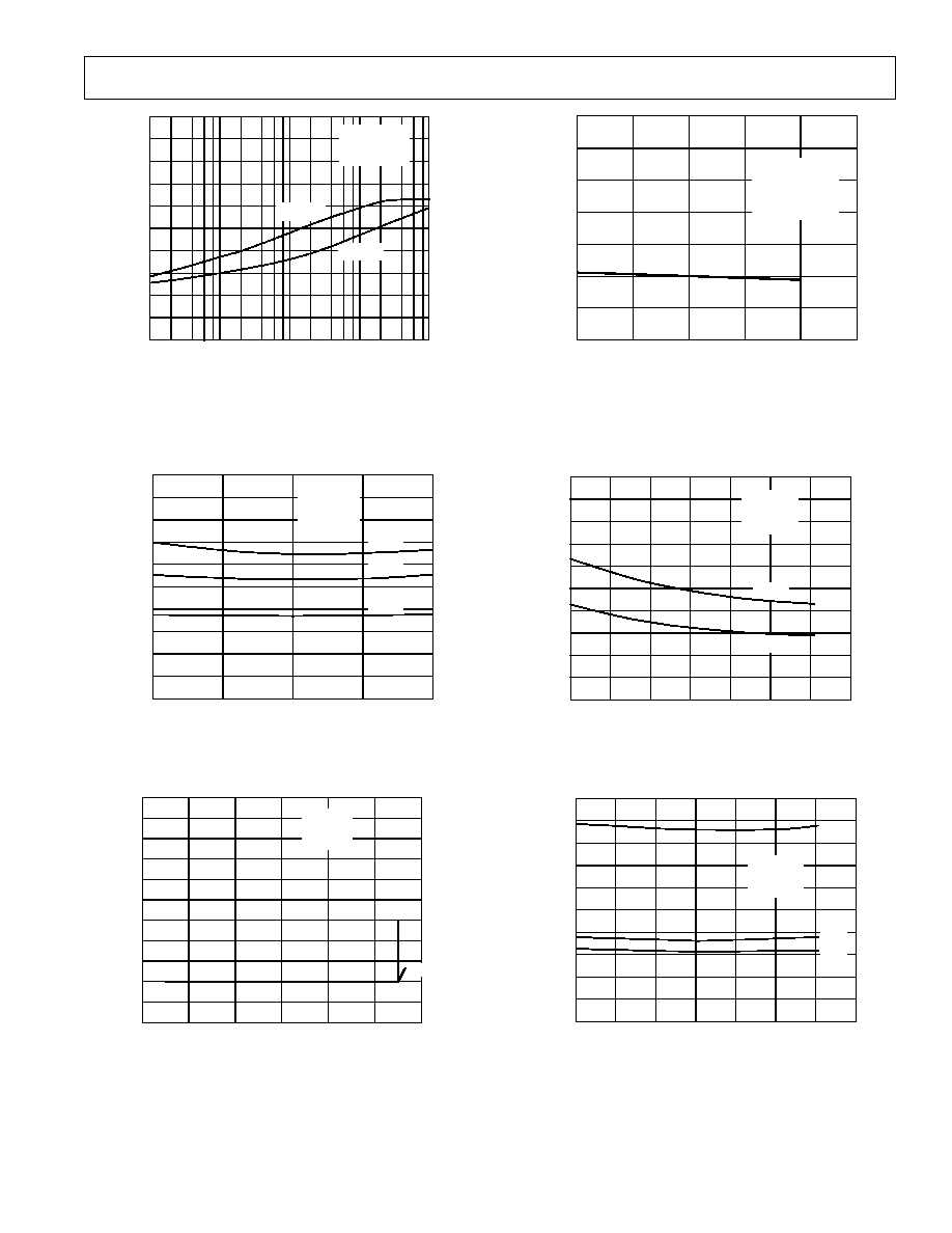
Figure 5. Frequency Response (V
S
=
±
12 V,
V
A
= 1 V rms, R
L
= 100 k
)
0Hz
MKR: 20 000Hz
CH A: 8.00
µ
V FS
1.00
µ
V/DIV
25kHz
BW: 150Hz
MKR: 0.11
µ
V/ Hz
Figure 6. SSM2404 Spectral Noise Density e
n
[5 Devices (20 Switches) Chained Together]
10
90
100
0%
10V
10V
5
µ
s
0V
0V
OUTPUT
INPUT
Figure 7. Square Wave Response (T
A
= +25
∞
C,
V
S
=
±
12 V, R
L
= 100 k
, f = 20 kHz)
9.5
7.0
6.0
100
1k
100k
10k
8.5
6.5
7.5
8.0
9.0
LOAD RESISTANCE ≠
OUTPUT VOLTAGE SWING ≠ V
RMS
T = 25
∞
C
V =
±
12V
f = 20kHz
A
S
Figure 8. Output Voltage Swing vs. Load Resistance
10
0
±
12
3
1
±
6
2
±
4
6
4
5
7
8
9
±
10
±
8
SUPPLY VOLTAGE ≠ Volts
OUTPUT VOLTAGE SWING ≠ V
RMS
T = 25
∞
C
R = 100k
f = 20kHz
0.1% THD + N
A
L
Figure 9. Output Voltage Swing vs. Supply Voltage
≠20
≠70
≠120
100
100k
10k
1k
10
≠60
≠50
≠40
≠30
≠110
≠100
≠90
≠80
FREQUENCY ≠ Hz
OFF ISOLATION ≠ dB
R = 100k
L
R = 10k
L
T = 25
∞
C
V =
±
12V
V = 50mV
RMS
A
S
A
Figure 10. OFF-Isolation vs. Frequency
SSM2404
REV. B
≠5≠
0
≠75
≠150
100
100k
10k
1k
10
≠60
≠45
≠30
≠15
≠135
≠120
≠105
≠90
FREQUENCY ≠ Hz
CROSSTALK ≠ dB
R = 100k
L
R = 10k
L
RMS
T = 25
∞
C
V =
±
12V
V = 50mV
A
S
A
Figure 11. Channel-to-Channel Crosstalk vs. Frequency
(Worst Case Conditions, as Measured Between
Switches 1 and 4, or 2 and 3)
50
0
10
≠5
10
≠10
30
20
40
5
0
ANALOG INPUT VOLTAGE ≠ Volts
ON RESISTANCE ≠
V =
±
12V
R =
I = 10mA
S
A
L
+85
∞
C
≠40
∞
C
+25
∞
C
Figure 12. ON Resistance vs. Analog Voltage
90
≠20
15
10
≠10
≠10
0
≠15
40
20
30
50
60
70
80
10
5
0
≠5
ANALOG INPUT VOLTAGE ≠ Volts
SWITCH LEAKAGE CURRENT ≠ mA
T = 25
∞
C
V =
±
12V
R =
A
S
L
V = 0.8V
IL
V = 2.4V
IH
Figure 13. Overvoltage Characteristics
50
≠20
10
≠10
≠5
0
≠10
40
20
30
10
5
0
V =
±
12V
V = 0.8V
R =
S
INL
L
≠40
∞
C TO +85
∞
C
ANALOG INPUT VOLTAGE ≠ Volts
SWITCH LEAKAGE CURRENT ≠ nA
Figure 14. Leakage Current vs. Analog Voltage
20
0
100
6
2
≠20
4
≠40
12
8
10
14
16
18
80
60
40
20
0
TEMPERATURE ≠
∞
C
SWITCHING TIME ≠ ms
V =
±
12V
V =
±
5V
R =
S
A
L
T
ON
T
OFF
Figure 15. Switching Time vs. Temperature
1.0
≠1.0
100
≠0.4
≠0.8
≠20
≠0.6
≠40
0.2
≠0.2
0
0.4
0.6
0.8
80
60
40
20
0
TEMPERATURE ≠
∞
C
SUPPLY CURRENT ≠ mA
I
SY+
I
SY≠
I
GND
V =
±
12V
V = GND
V = 2.4V
S
A
INH
Figure 16. Supply Current vs. Temperature