 | ÐлекÑÑоннÑй компоненÑ: SSM2475-B | СкаÑаÑÑ:  PDF PDF  ZIP ZIP |
SSM2275/2475 Data Sheet
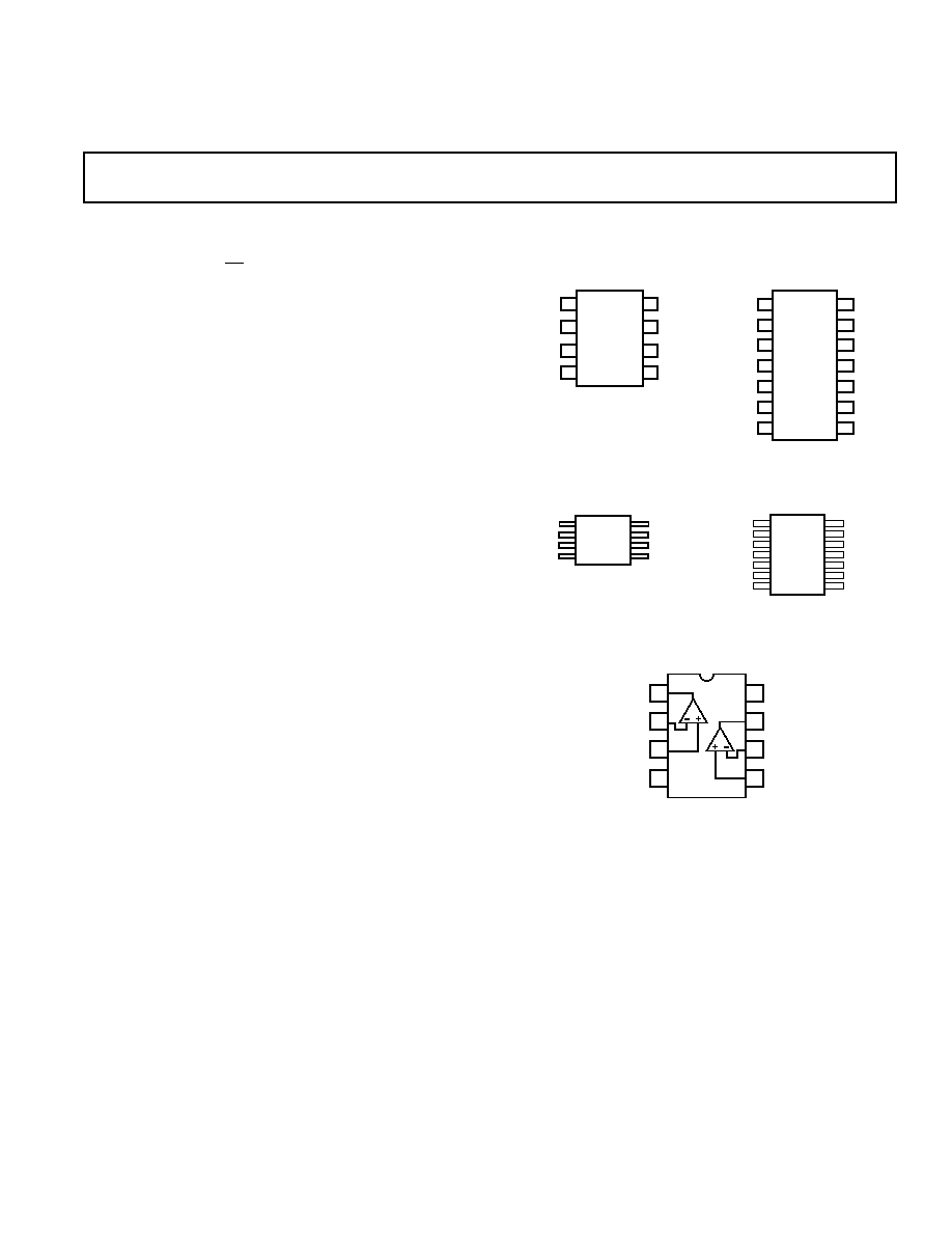
8-Lead Narrow Body SOIC 14-Lead Narrow Body SOIC
(SO-8)
(R-14)
8-Lead microSOIC 14-Lead TSSOP
(RM-8) (RU-14)
8-Lead Plastic DIP
(N-8)
REV. A
Information furnished by Analog Devices is believed to be accurate and
reliable. However, no responsibility is assumed by Analog Devices for its
use, nor for any infringements of patents or other rights of third parties
which may result from its use. No license is granted by implication or
otherwise under any patent or patent rights of Analog Devices.
a
Rail-to-Rail Output
Audio Amplifiers
SSM2275/SSM2475*
One Technology Way, P.O. Box 9106, Norwood. MA 02062-9106, U.S.A.
Tel: 781/329-4700 World Wide Web Site: http://www.analog.com
Fax: 781/326-8703 © Analog Devices, Inc., 1999
GENERAL DESCRIPTION
The SSM2275 and SSM2475 use the Butler Amplifier front
end, which combines both bipolar and FET transistors to offer
the accuracy and low noise performance of bipolar transistors
and the slew rates and sound quality of FETs. This product
family includes dual and quad rail-to-rail output audio amplifi-
ers that achieve lower production costs than the industry stan-
dard OP275 (the first Butler Amplifier offered by Analog
Devices). This lower cost amplifier also offers operation from a
single 5 V supply, in addition to conventional
±
15 V supplies.
The ac performance meets the needs of the most demanding au-
dio applications, with 8 MHz bandwidth, 12 V/
µ
s slew rate and
extremely low distortion.
The SSM2275 and SSM2475 are ideal for application in high
performance audio amplifiers, recording equipment, synthesiz-
ers, MIDI instruments and computer sound cards. Where cas-
caded stages demand low noise and predictable performance,
SSM2275 and SSM2475 are a cost effective solution. Both are
stable even when driving capacitive loads.
The ability to swing rail-to-rail at the outputs (see Applications sec-
tion) and operate from low supply voltages enables designers to at-
tain high quality audio performance, even in single supply systems.
The SSM2275 and SSM2475 are specified over the extended
industrial (40
°
C to +85
°
C) temperature range. The SSM2275 is
available in 8-lead plastic DIPs, SOICs, and microSOIC surface-
mount packages. The SSM2475 is available in narrow body
SOICs and thin shrink small outline (TSSOP) surface-mount
packages.
*Protected by U.S. Patent No. 5,101,126.
FEATURES
Single or Dual-Supply Operation
Excellent Sonic Characteristics
Low Noise: 7 nV/
Hz
Low THD: 0.0006%
Rail-to-Rail Output
High Output Current: 50 mA
Low Supply Current: 1.7 mA/Amplifier
Wide Bandwidth: 8 MHz
High Slew Rate: 12 V/ s
No Phase Reversal
Unity Gain Stable
Stable Parameters Over Temperature
APPLICATIONS
Multimedia Audio
Professional Audio Systems
High Performance Consumer Audio
Microphone Preamplifier
MIDI Instruments
PIN CONFIGURATIONS
1
2
3
4
8
7
6
5
(Not to Scale)
OUT A
IN A
+IN A
V
OUT B
IN B
+IN B
V+
SSM2275
OUT A
IN A
+IN A
V+
IN D
+IN D
V
OUT D
1
2
3
4
5
6
7
14
13
12
11
10
9
8
+IN B
IN B
OUT B
IN C
OUT C
+IN C
SSM2475
(Not to Scale)
IN A
+IN A
V
OUT B
IN B
+IN B
V+
1
4
5
8
SSM2275
OUT A
OUT A
IN A
+IN A
V+
IN D
+IN D
V
OUT D
1
14
+IN B
IN B
OUT B
IN C
OUT C
+IN C
7
8
SSM2475
1
2
3
4
8
7
6
5
(Not to
Scale)
SSM2275
OUT A
IN A
+IN A
V
+IN B
IN B
OUT B
V+
REV. A
2
SSM2275/SSM2475SPECIFICATIONS
ELECTRICAL CHARACTERISTICS
Parameter
Symbol
Conditions
Min
Typ
Max
Units
INPUT CHARACTERISTICS
Offset Voltage
V
OS
1
4
mV
40
°
C
T
A
+85
°
C
1
6
mV
Input Bias Current
I
B
250
400
nA
40
°
C
T
A
+85
°
C
300
500
nA
Input Offset Current
I
OS
5
75
nA
40
°
C
T
A
+85
°
C
15
125
nA
Input Voltage Range
V
IN
V
S
=
±
15 V
14
+14
V
Common-Mode Rejection Ratio
CMRR
12.5 V
V
CM
+12.5 V
80
100
dB
40
°
C
T
A
+85
°
C,
12.5 V
V
CM
+12.5 V
80
100
V/mV
A
VO
R
L
= 2 k
, 12 V
V
O
+12 V
100
240
V/mV
40
°
C
T
A
+85
°
C
80
120
V/mV
OUTPUT CHARACTERISTICS
Output Voltage, High
V
OH
I
L
20 mA
14
14.5
V
40
°
C
T
A
+85
°
C
14.5
14.7
V
Output Voltage, Low
V
OL
I
L
= 20 mA
14
13.5
V
I
L
= 10 mA
14.6 14.4
V
I
L
= 10 mA, 40
°
C
T
A
+85
°
C
14.3 13.9
V
Output Short Circuit Current Limit
I
SC
±
25
±
50
±
75
mA
40
°
C
T
A
+85
°
C
±
17
±
40
±
80
mA
POWER SUPPLY
Power Supply Rejection Ratio
PSRR
±
2.5 V
V
S
±
18 V
85
110
dB
40
°
C
T
A
+85
°
C
80
105
dB
Supply Current/Amplifier
I
SY
V
O
= 0 V
1.7
2.9
mA
40
°
C
T
A
+85
°
C
1.75
3.0
mA
DYNAMIC PERFORMANCE
Total Harmonic Distortion
THD
R
L
= 10 k
, f = 1 kHz, V
O
= 1 V rms
0.0006
%
Slew Rate
SR
R
L
= 2 k
50 pF
9
12
V/
µ
s
Gain Bandwidth Product
GBW
8
MHz
Channel Separation
CS
R
L
= 2 k
, f =1 kHz
128
dB
NOISE PERFORMANCE
Voltage Noise Spectral Density
e
n
f > 1 kHz
8
nV/
Hz
Current Noise Spectral Density
i
n
f > 1 kHz
< 1
pA/
Hz
Specifications subject to change without notice.
(V
S
= 15 V, T
A
= 25 C, V
CM
= 0 V unless otherwise noted)
ELECTRICAL CHARACTERISTICS
Parameter
Symbol
Conditions
Min
Typ
Max
Units
INPUT CHARACTERISTICS
Offset Voltage
V
OS
1
4
mV
40
°
C
T
A
+85
°
C
1
6
mV
Input Bias Current
I
B
250
400
nA
40
°
C
T
A
+85
°
C
300
500
nA
Input Offset Current
I
OS
5
75
nA
40
°
C
T
A
+85
°
C
15
125
nA
Input Voltage Range
V
IN
0.3
4.7
V
Common-Mode Rejection Ratio
CMRR
+0.8 V
V
CM
+2 V
85
dB
40
°
C
T
A
+85
°
C
80
dB
A
VO
R
L
= 2 k
, 0.5 V
V
O
+4.5 V
25
60
V/mV
40
°
C
T
A
+85
°
C
20
50
V/mV
OUTPUT CHARACTERISTICS
Output Voltage, High
V
OH
I
L
15 mA
4.2
4.5
V
I
L
10 mA, 40
°
C
T
A
+85
°
C
4.5
4.8
V
Output Voltage, Low
V
OL
I
L
15 mA
0.6
1.0
V
I
L
10 mA
0.3
0.5
V
I
L
10 mA, 40
°
C
T
A
+85
°
C
0.7
1.1
V
Output Short Circuit Current Limit
I
SC
40
°
C
T
A
+85
°
C
40
mA
POWER SUPPLY
Supply Current/Amplifier
I
SY
V
O
= 0 V
1.7
2.9
mA
40
°
C
T
A
+85
°
C
1.75
3.0
mA
DYNAMIC PERFORMANCE
Total Harmonic Distortion
THD
R
L
= 10 k
, f = 1 kHz, V
O
= 1 V rms
0.0006
%
Slew Rate
SR
R
L
= 2 k
50 pF
12
V/
µ
s
Gain Bandwidth Product
GBW
R
L
= 2 k
10 pF
6
MHz
Channel Separation
CS
R
L
= 2 k
, f =1 kHz
128
dB
NOISE PERFORMANCE
Voltage Noise Spectral Density
e
n
f > 1 kHz
8
nV/
Hz
Current Noise Spectral Density
i
n
f > 1 kHz
< 1
pA/
Hz
Specifications subject to change without notice.
REV. A
3
SSM2275/SSM2475
(V
S
= 5 V, T
A
= 25 C, V
CM
= 2.5 V unless otherwise noted)
SSM2275/SSM2475
REV. A
4
ABSOLUTE MAXIMUM RATINGS
1
Supply Voltage (V
S
) . . . . . . . . . . . . . . . . . . . . . . . . . . . .
±
18 V
Input Voltage (V
IN
) . . . . . . . . . . . . . . . . . . . . . . . . . . . .
±
15 V
Differential Input Voltage
2
. . . . . . . . . . . . . . . . . . . . . . .
±
15 V
Storage Temperature Range . . . . . . . . . . . .
65
°
C to 150
°
C
Operating Temperature Range . . . . . . . . . . .
40
°
C to 85
°
C
Junction Temperature Range . . . . . . . . . . . .
65
°
C to 150
°
C
Lead Temperature Range (Soldering, 60 sec) . . . . . . .
300
°
C
ESD Susceptibility . . . . . . . . . . . . . . . . . . . . . . . . . . . . 2,000 V
NOTES
1
Stresses above those listed under Absolute Maximum Ratings may cause perma -
nent damage to the device. This is a stress rating only; the functional operation of
the device at these or any other conditions above those indicated in the opera tional
sections of this specification is not implied. Exposure to absolute maximum rating
conditions for extended periods may affect device reliability.
2
For supplies less than
±
15 V, the input voltage and differential input voltage
must be less than
±
15 V.
Package Type
JA
*
JC
Units
8-Lead Plastic DIP
103
43
°
C/W
8-Lead SOIC
158
43
°
C/W
8-Lead microSOIC
206
43
°
C/W
14-Lead SOIC
120
36
°
C/W
14-Lead TSSOP
180
35
°
C/W
*
JA
is specified for the worst case conditions, i.e., for device in socket for DIP
packages and soldered onto a circuit board for surface mount packages.
ORDERING GUIDE
Temperature
Package
Package
Model
Range
Description
Options
SSM2275P
40
°
C to +85
°
C
8-Lead PDIP
N-8
SSM2275S
40
°
C to +85
°
C
8-Lead SOIC
SO-8
SSM2275RM
40
°
C to +85
°
C
8-Lead microSOIC
RM-8
SSM2475S
40
°
C to +85
°
C
14-Lead SOIC
R-14
SSM2475RU
40
°
C to +85
°
C
14-Lead TSSOP
RU-14
CAUTION
ESD (electrostatic discharge) sensitive device. Electrostatic charges as high as 4000 V readily
accumulate on the human body and test equipment and can discharge without detection.
Although the SSM2275/SSM2475 features proprietary ESD protection circuitry, permanent
damage may occur on devices subjected to high energy electrostatic discharges. Therefore, proper
ESD precautions are recommended to avoid performance degradation or loss of functionality.
WARNING!
ESD SENSITIVE DEVICE
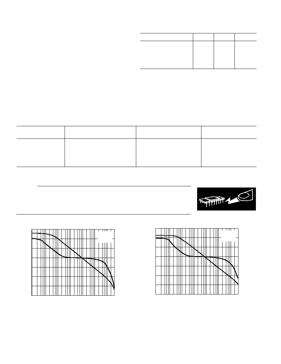
FREQUENCY Hz
100
80
40
10
1M
100
GAIN dB
1k
10k
100k
60
40
20
0
20
10M 40M
PHASE Degrees
225
180
90
135
90
45
0
45
V
S
= 2.5V
R
L
= 2k
C
L
= 10pF
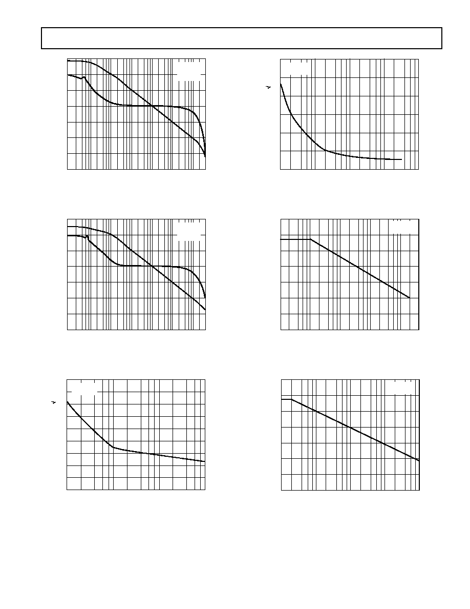
Figure 1. Phase/Gain vs. Frequency
FREQUENCY Hz
100
80
40
10
1M
100
GAIN dB
1k
10k
100k
60
40
20
0
20
10M 40M
PHASE Degrees
225
180
90
135
90
45
0
45
V
S
= 2.5V
R
L
= 600
C
L
= 10pF
Figure 2. Phase/Gain vs. Frequency
FREQUENCY Hz
100
80
40
10
1M
100
GAIN dB
1k
10k
100k
60
40
20
0
20
10M 40M
PHASE De
g
rees
225
180
90
135
90
45
0
45
V
S
= 15V
R
L
= 2k
C
L
= 10pF
Figure 3. Phase/Gain vs. Frequency
FREQUENCY Hz
100
80
40
10
1M
100
GAIN dB
1k
10k
100k
60
40
20
0
20
10M 40M
PHASE De
g
rees
225
180
90
135
90
45
0
45
V
S
= 15V
R
L
= 600
C
L
= 10pF
Figure 4. Phase/Gain vs. Frequency
FREQUENCY Hz
2.0
1.8
0.2
10
10k
100
CURRENT NOISE DENSITY pA/
Hz
1k
1.6
1.4
0.6
1.2
1.0
0.8
0.4
V
S
= 15V
T
A
= 25 C
Figure 5. SSM2275 Current Noise Density vs. Frequency
FREQUENCY Hz
60
50
0
10
100k
100
VOLTAGE NOISE DENSITY nV/
Hz
1k
10k
40
30
10
20
V
S
= 15V
T
A
= 25 C
Figure 6. SSM2275 Voltage Noise Density (Typical)
FREQUENCY Hz
140
120
0
100
30M
1k
COMMON MODE REJECTION dB
10k
1M
10M
100
80
60
40
20
V
S
= 15V
T
A
= 25 C
Figure 7. Common-Mode Rejection vs. Frequency
FREQUENCY Hz
140
120
0
100
10M
1k
POWER SUPPLY REJECTION dB
10k
1M
100
80
60
40
20
V
S
= 15V
T
A
= 25 C
Figure 8. Power Supply Rejection vs. Frequency
Typical CharacteristicsSSM2275/SSM2475
REV. A
5
SSM2275/SSM2475
REV. A
6
FREQUENCY kHz
100
130
160
0
22
2
AMPLITUDE dBV
4
6
8
10
12
14
16
18
20
110
120
140
150
V
SY
= +5V
A
V
= +1
R
L
= 100k
V
IN
= 0dBV
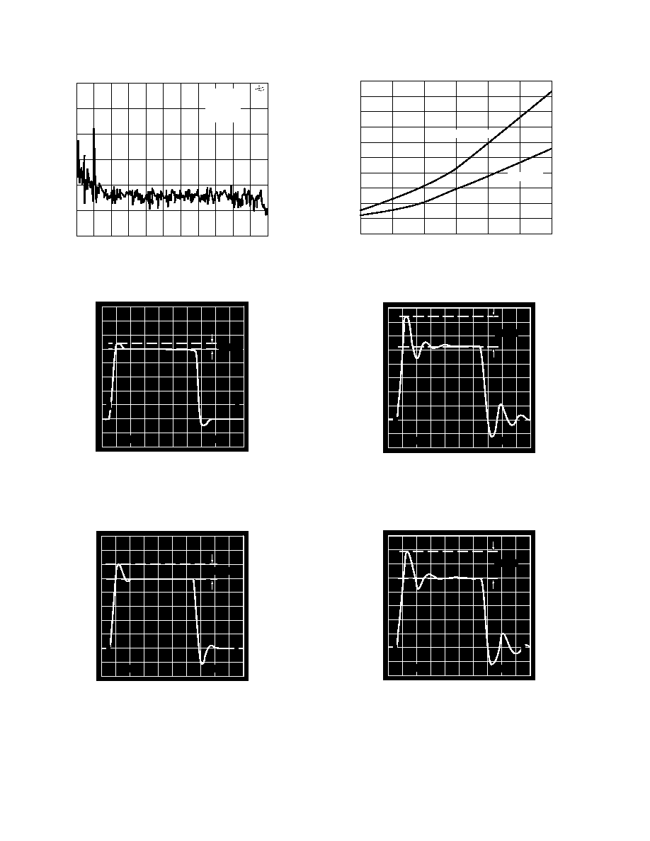
Figure 9. THD vs. Frequency (FFT)
11.0mV
0
0
200ns
20mV
Figure 10. Small Signal Response; R
L
= 600
, C
L
= 0 pF,
V
S
=
±
2.5 V, A
V
= +1, V
IN
= 100 mV p-p
22.5mV
0
0
200ns
20mV
Figure 11. Small Signal Response; R
L
= 600
, C
L
= 100 pF,
V
S
=
±
2.5 V, A
V
= +1, V
IN
= 100 mV p-p
SSM2275/SSM2475Typical Characteristics
REV. A
6
LOAD CURRENT mA
1.0
0.8
0
5
20
V
OH
, V
OL
(VOLTS-TO-RAIL) V
10
15
0.6
0.4
0.2
0.9
0.7
0.5
0.3
0.1
V
OUT
(V+)
V
OUT
(V)
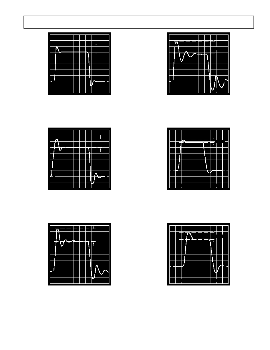
Figure 12. Headroom (V
OH
and V
OL
-to-Rails), T
A
= +25
°
C
29.5mV
0
200ns
20mV
0
Figure 13. Small Signal Response; R
L
= 600
, C
L
= 200 pF,
V
S
=
±
2.5 V, A
V
= +1, V
IN
= 100 mV p-p
35.5mV
0
0
200ns
20mV
Figure 14. Small Signal Response; R
L
= 600
, C
L
= 300 pF,
V
S
=
±
2.5 V, A
V
= +1, V
IN
= 100 mV p-p
SSM2275/SSM2475
REV. A
7
17.5mV
0
0
200ns
20mV
Figure 15. Small Signal Response; R
L
= 2 k
, C
L
= 0 pF,
V
S
=
±
2.5 V, A
V
= +1, V
IN
= 100 mV p-p
31.0mV
0
0
200ns
20mV
Figure 16. Small Signal Response; R
L
= 2 k
, C
L
= 100 pF,
V
S
=
±
2.5 V, A
V
= +1, V
IN
= 100 mV p-p
38.0mV
0
0
200ns
20mV
Figure 17. Small Signal Response; R
L
= 2 k
, C
L
= 200 pF,
V
S
=
±
2.5 V, A
V
= +1, V
IN
= 100 mV p-p
43.0mV
200ns
20mV
0
0
Figure 18. Small Signal Response; R
L
= 2 k
, C
L
= 300 pF,
V
S
=
±
2.5 V, A
V
= +1, V
IN
= 100 mV p-p
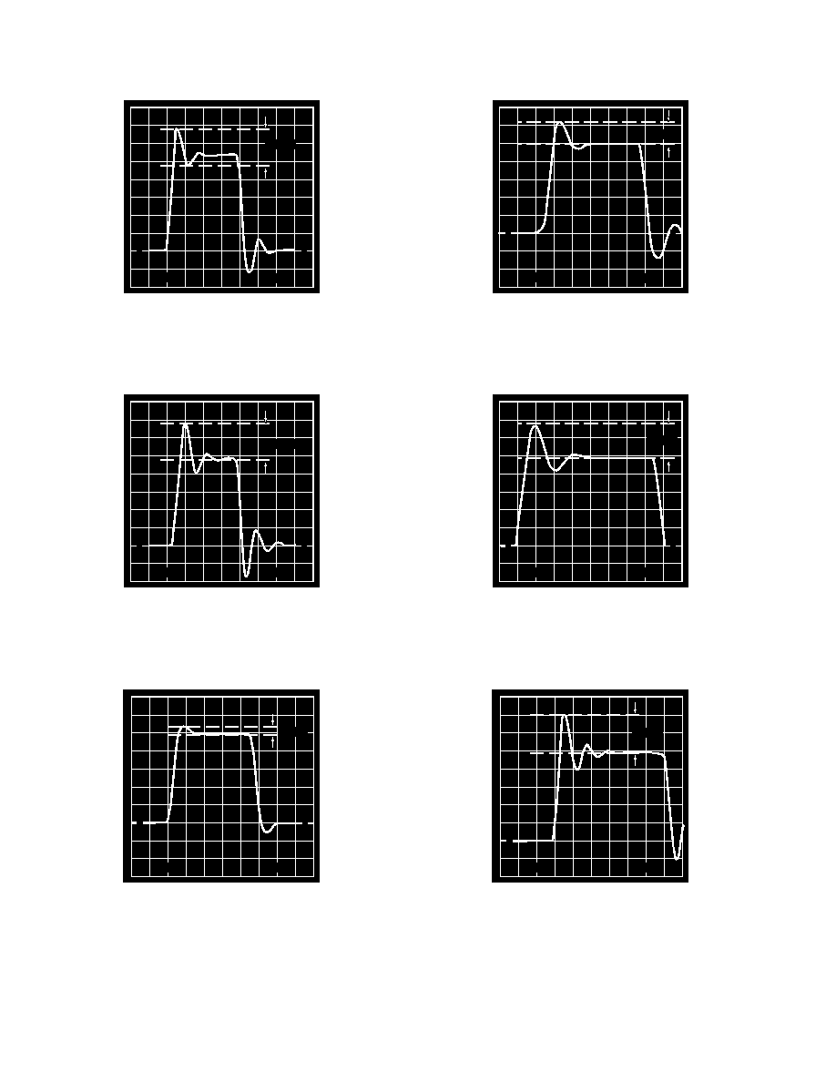
10.5mV
0
0
100ns
20mV
Figure 19. Small Signal Response; R
L
= 600
, C
L
= 0 pF,
V
S
=
±
15 V, A
V
= +1, V
IN
= 100 mV p-p
22.5mV
0
0
100ns
20mV
Figure 20. Small Signal Response; R
L
= 600
, C
L
= 100 pF,
V
S
=
±
15 V, A
V
= +1, V
IN
= 100 mV p-p
SSM2275/SSM2475Typical Characteristics
REV. A
8
29.0mV
0
0
200ns
20mV
Figure 21. Small Signal Response; R
L
= 600
, C
L
= 200 pF,
V
S
=
±
15 V, A
V
= +1, V
IN
= 100 mV p-p
35.5mV
0
0
200ns
20mV
Figure 22. Small Signal Response; R
L
= 600
, C
L
= 300 pF,
V
S
=
±
15 V, A
V
= +1, V
IN
= 100 mV p-p
13.0mV
0
0
100ns
20mV
Figure 23. Small Signal Response; R
L
= 2 k
, C
L
= 0 pF,
V
S
=
±
15 V, A
V
= +1, V
IN
= 100 mV p-p
28.0mV
0
0
100ns
20mV
Figure 24. Small Signal Response; R
L
= 2 k
, C
L
= 100 pF,
V
S
=
±
15 V, A
V
= +1, V
IN
= 100 mV p-p
100ns
20mV
36.5mV
0
0
Figure 25. Small Signal Response; R
L
= 2 k
, C
L
= 200 pF,
V
S
=
±
15 V, A
V
= +1, V
IN
= 100 mV p-p
42.0mV
0
0
200ns
20mV
Figure 26. Small Signal Response; R
L
= 2 k
, C
L
= 300 pF,
V
S
=
±
15 V, A
V
= +1, V
IN
= 100 mV p-p
SSM2275/SSM2475
REV. A
9
±
7 V, then the input current should be limited to less than
±
5 mA. This can be easily done by placing a resistor in series
with both inputs. The minimum value of the resistor can be
determined by:
R
V
IN
DIFF MAX
=
-
,
.
7
0 01
(1)
There are also ESD protection diodes that are connected from
each input to each power supply rail. These diodes are normally
reversed biased, but will turn on if either input voltage exceeds
either supply rail by more than 0.6 V. Again, should this condi-
tion occur the input current should be limited to less than
±
5 mA. The minimum resistor value should then be:
R
V
mA
IN
IN MAX
=
,
5
(2)
In practice, R
IN
should be placed in series with both inputs to
reduce offset voltages caused by input bias current. This is
shown in Figure 28.
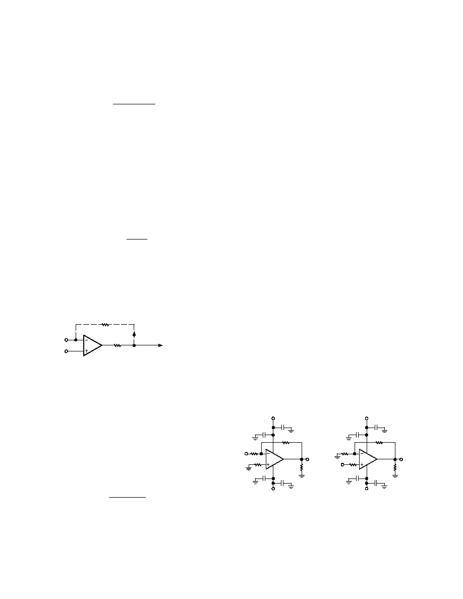
R
IN
R
IN
V+
V
Figure 28. Using Resistors for Input Overcurrent Protection
Output Voltage Phase Reversal
The SSM2275/SSM2475 was designed to have a wide common-
mode range and is immune to output voltage phase reversal with
an input voltage within the supply voltages of the device. How-
ever, if either of the device's inputs exceeds 0.6 V above the posi-
tive voltage supply, the output could exhibit phase reversal.
This is due to the input transistor's BC junction becoming for-
ward biased, causing the polarity of the input terminals of the
device to switch.
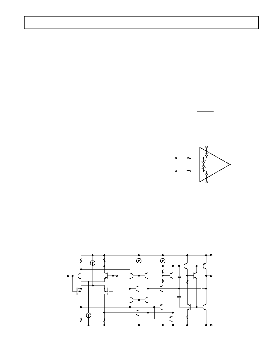
THEORY OF OPERATION
The SSM2275 and SSM2475 are low noise and low distortion
rail-to-rail output amplifiers that are excellent for audio applica-
tions. Based on the OP275 audiophile amplifier, the SSM2275/
SSM2475 offers many similar performance characteristics with
the advantage of a rail-to-rail output from a single supply
source. Its low input voltage noise figure of 7 nV/
Hz allows the
device to be used in applications requiring high gain, such as
microphone preamplifiers. Its 11 V/
µ
s slew rate also allows the
SSM2275/SSM2475 to produce wide output voltage swings
while maintaining low distortion. In addition, its low harmonic
distortion figure of 0.0006% makes the SSM2275 and
SSM2475 ideal for high quality audio applications.
Figure 27 shows the simplified schematic for a single amplifier.
The amplifier contains a Butler Amplifier at the input. This
front-end design uses both bipolar and MOSFET transistors in
the differential input stage. The bipolar devices, Q1 and Q2,
improve the offset voltage and achieve the low noise perfor-
mance, while the MOS devices, M1 and M2, are used to obtain
higher slew rates. The bipolar differential pair is biased with a
proportional-to-absolute-temperature (PTAT) bias source, IB1,
while the MOS differential pair is biased with a non-PTAT
source, IB2. This results in the amplifier having a constant gain-
bandwidth product and a constant slew rate over temperature.
The amplifier also contains a rail-to-rail output stage that can
sink or source up to 50 mA of current. As with any rail-to-rail
output amplifier the gain of the output stage, and consequently
the open loop gain of the amplifier, is proportional to the load
resistance. With a load resistance of 50 k
, the dc gain of the
amplifier is over 110 dB. At load currents less than 1 mA, the
output of the amplifier can swing to within 30 mV of either sup-
ply rail. As load current increases, the maximum voltage swing
of the output will decrease. This is due to the collector to emit-
ter saturation voltage of the output transistors increasing with an
increasing collector current.
Input Overvoltage Protection
The maximum input differential voltage that can be applied to
the SSM2275/SSM2475 is
±
7 V. A pair of internal back-to-back
Zener diodes are connected across the input terminals. This
prevents emitter-base junction breakdown from occurring to the
input transistors, Q1 and Q2, when very large differential volt-
ages are applied. If the device's differential voltage could exceed
Q2
IN+
IB2
IN
Q1
M2
M1
IB1
CFI
OUT
V
CC
V
EE
Figure 27. Simplified Schematic
SSM2275/SSM2475
REV. A
10
This phase reversal can be prevented by limiting the input cur-
rent to +1 mA. This can be done by placing a resistor in series
with the input terminal that is expected to be overdriven. The
series resistance should be at least:
R
V
mA
IN
IN MAX
=
-
,
.
0 6
1
(3)
An equivalent resistor should be placed in series with both in-
puts to prevent offset voltages due to input bias currents, as
shown in Figure 28.
Output Short Circuit Protection
To achieve high quality rail-to-rail performance, the output of
the SSM2275/SSM2475 is not short-circuit protected. Shorting
the output may damage or destroy the device when excessive
voltages or currents are applied. To protect the output stage, the
maximum output current should be limited to
±
40 mA. Placing
a resistor in series with the output of the amplifier as shown in
Figure 29, the output current can be limited. The minimum
value for R
X
can be found from Equation 4.
R
V
mA
X
SY
=
40
(4)
For a +5 V single supply application, R
X
should be at least
125
. Because R
X
is inside the feedback loop, V
OUT
is not
affected. The trade off in using R
X
is a slight reduction in output
voltage swing under heavy output current loads. R
X
will also
increase the effective output impedance of the amplifier to
R
O
+ R
X
, where R
O
is the output impedance of the device.
R
FB
FEEDBACK
R
X
125
V
OUT
A1 = 1/2 SSM2275
A1
Figure 29. Output Short Circuit Protection Configuration
Power Dissipation Considerations
While many designers are constrained to use very small and low
profile packages, reliable operation demands that the maximum
junction temperatures not be exceeded. A simple calculation
will ensure that your equipment will enjoy reliable operation
over a long lifetime. Modern IC design allows dual and quad
amplifiers to be packaged in SOIC and microSOIC packages,
but it is the responsibility of the designer to determine what the
actual junction temperature will be, and prevent it from exceed-
ing the 150
°
C. Note that while the
JC
is similar between pack-
age options, the
JA
for the SOIC and TSSOP are nearly double
the PDIP. The calculation of maximum ambient temperature is
relatively simple to make.
P
T
T
MAX
I MAX
A
A
=
-
,
J
(5)
For example, with the 8-lead SOIC, the calculation gives a
maximum internal power dissipation (for all amplifiers, worst
case) of P
MAX
= (150
°
C 85
°
C)/158
°
C/W = 0.41 W. For the
DIP package, a similar calculation indicates that 0.63 W (ap-
proximately 50% more) can be safely dissipated. Note that am-
bient temperature is defined as the temperature of the PC board
to which the device is connected (in the absence of radiated or
convected heat loss). It is good practice to place higher power
devices away from the more sensitive circuits. When in doubt,
measure the temperature in the vicinity of the SSM2275 with a
thermocouple thermometer.
Maximizing Low Distortion Performance
Because the SSM2275/SSM2475 is a very low distortion amplifier,
careful attention should be given to the use of the device to prevent
inadvertently introducing distortion. Source impedances seen by
both inputs should be made equal, as shown in Figure 28, with
R
B
= R1 R
F
for minimum distortion. This eliminates any offset
voltages due to varying bias currents. Proper power supply
decoupling reduces distortion due to power supply variations.
Because the open loop gain of the amplifier is directly dependent
on the load resistance, loads of less than 10 k
will increase the
distortion of the amplifier. This is a trait of any rail-to-rail op
amp. Increasing load capacitance will also increase distortion.
It is recommended that any unused amplifiers be configured as a
unity gain follower with the noninverting input tied to ground.
This minimizes the power dissipation and any potential crosstalk
from the unused amplifier.
As with many FET-type amplifiers, the PMOS devices in the
input stage exhibit a gate-to-source capacitance that varies with
the common mode voltage. In an inverting configuration, the in-
verting input is held at a virtual ground and the common-mode
voltage does not vary. This eliminates distortion due to input
capacitance modulation. In noninverting applications, the gate-
to-source voltage is not constant, and the resulting capacitance
modulation can cause a slight increase in distortion.
Figure 30 shows a unity gain inverter and a unity gain follower
configuration. Figure 31 shows an FFT of the outputs of these
amplifiers with a 1 kHz sine wave. Notice how the largest har-
monic amplitude (2nd harmonic) is 120 dB below the funda-
mental (0.0001%) in the inverting configuration.
SSM2275
R
FB
V
OUT
R
L
V
IN
R1
0.1 F
10 F
V
0.1 F
10 F
V+
R
B
SSM2275
R
FB
V
OUT
R
L
V
IN
R1
0.1 F
10 F
V
0.1 F
10 F
V+
R
B
Figure 30. Basic Inverting and Noninverting Amplifiers
SSM2275/SSM2475
REV. A
11
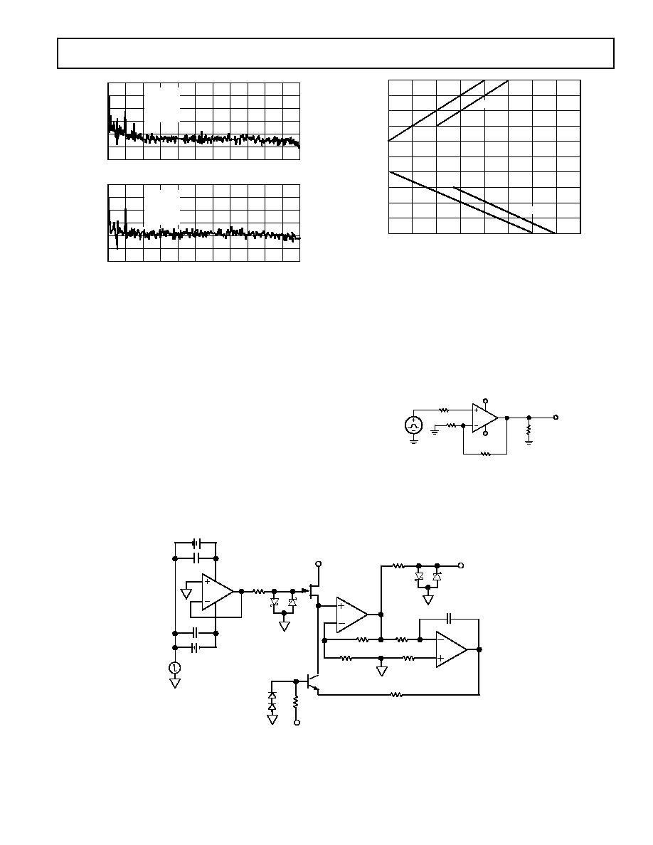
FREQUENCY kHz
100
130
160
0
22
NOISE dBV
10
20
110
120
140
150
V
SY
= 5V
A
V
= 1
R
L
= 100k
V
IN
= 0dBV
FREQUENCY kHz
100
130
160
0
22
NOISE dBV
10
20
110
120
140
150
V
SY
= 5V
A
V
= 1
R
L
= 100k
V
IN
= 0dBV
Figure 31. Spectral Graph of Amplifier Outputs
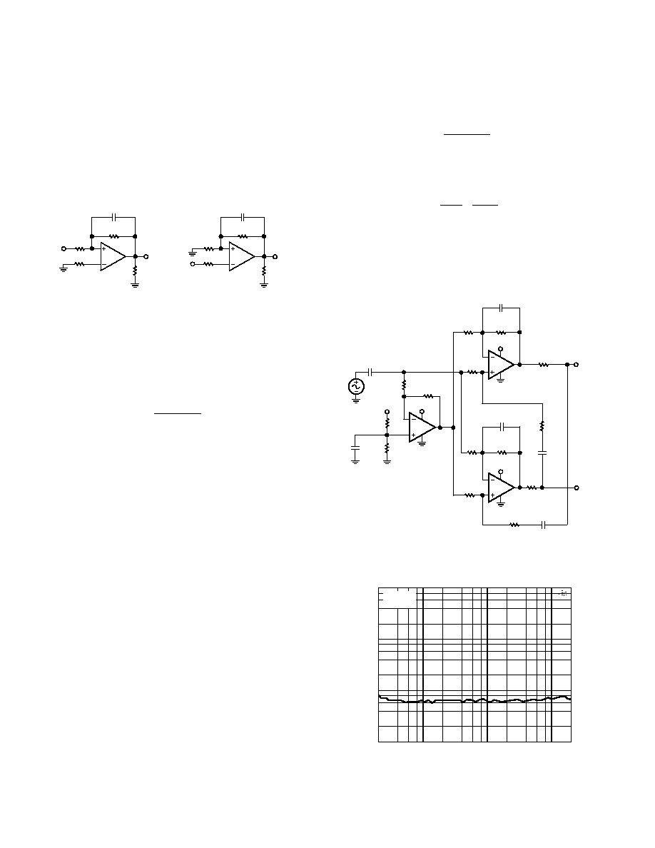
Settling Time
The high slew rate and wide gain-bandwidth product of the
SSM2275 and SSM2475 amplifiers result in fast settling times
(t
S
< 1
µ
s) that are suitable for 16- and 20-bit applications. The
test circuit used to measure the settling time of the SSM2275/
SSM2475 is shown in Figure 32. This test method has advan-
tages over false-sum node techniques of measuring settling times
in that the actual output of the amplifier is measured, instead of
an error voltage at the sum node. Common-mode settling ef-
fects are also taken into account in this circuit in addition to
slew rate and bandwidth factors.
The output waveform of the device under test is clamped by
Schottky diodes and buffered by the JFET source follower. The
signal is amplified by a factor of ten by the OP260 current feed-
back amplifier and then Schottky-clamped at the output to the
oscilloscope. The 2N2222 transistor sets up the bias current for
the JFET and the OP41 is configured as a fast integrator, pro-
viding overall dc offset nulling at the output.
SETTLING TIME ns
10
6
10
400
600
STEP SIZE V
800
1000
1200
2
2
6
8
4
0
4
8
0.01%
0.1%
0.01%
Figure 33. Settling Time vs. Step Size
Overdrive Recovery
The overdrive, or overload, recovery time of an amplifier is the time
required for the output voltage to return to a rated output voltage
from a saturated condition. This recovery time can be important in
applications where the amplifier must recover quickly after a large
transient event, or overload. The circuit in Figure 34 was used to
evaluate the recovery time for the SSM2275/SSM2475. Also shown
are the input and output voltages. It takes approximately 0.5
µ
s for
the device to recover from output overload.
R1
1k
R
S
909
R
F
10k
+5V
5V
R
L
10k
V
OUT
V
IN
2V p-p
10kHz
Figure 34. Overload Recovery Time Test Circuit
9V15V
0.1 F
V+
5V
R
L
1k
D1
D2
+15V
2N4416
1k
D3
D4
OUTPUT
(TO SCOPE)
1 F
10k
IC2
R
F
2k
750
2N2222A
15k
15V
1N4148
DUT
1/2 OP260AJ
9V15V
0.1 F
10k
+
+
SCHOTTKY DIODES D1D4 ARE
HEWLETT-PACKARD HP5082-2835
IC1 IS 1/2 OP260AJ
IC2 IS PMI OP41EJ
V
R
G
222
Figure 32. Settling Time Test Fixture
SSM2275/SSM2475
REV. A
12
Capacitive Loading
The output of the SSM2275/SSM2475 can tolerate a degree of
capacitive loading. However, under certain conditions, a heavy
capacitive load could create excess phase shift at the output and
put the device into oscillation. The degree of capacitive loading
is dependent on the gain of the amplifier. At unity gain, the am-
plifier could become unstable at loads greater than 600 pF. At
gain greater than unity, the amplifier can handle a higher degree
of capacitive load without oscillating. Figure 35 shows how to
configure the device to prevent oscillations from occurring.
SSM2275
C
L
R
FB
C
FB
R
I
R
B
50k
V
IN
INVERTING GAIN AMPLIFIER
V
OUT
SSM2275
C
L
R
FB
C
FB
R
I
R
B
50k
V
IN
NONINVERTING GAIN AMPLIFIER
V
OUT
Figure 35. Configurations for Driving Heavy Capacitive
Loads
R
B
should be at least 50 k
. To minimize offset voltage, the
parallel combination of R
FB
and R
I
should be equal to R
B
. Set-
ting a minimum C
F
of 15 pF bandlimits the amplifier enough to
eliminate any oscillation problems from any sized capacitive
load. The low-pass frequency is determined by:
f
R C
dB
FB
F
-
=
3
1
2
(6)
With R
FB
= 50 k
and C
F
= 15 pF, this results in an amplifier
with a 210 kHz bandwidth that can be used with any capacitive
load. If the amplifier is being used in a noninverting unity gain
configuration and R
I
is omitted, C
FB
should be at least 100 pF.
If the offset voltage can be tolerated at the output, R
FB
can be
replaced by a short and C
FB
can be removed entirely. With the
typical input bias current of 200 nA and R
B
= 50 k
, the in-
crease in offset voltage would be 10 mV. This configuration will
stabilize the amplifier under all capacitive loads.
Single Supply Differential Line Driver
Figure 36 shows a single supply differential line driver circuit
that can drive a 600
load with less than 0.001% distortion.
The design mimics the performance of a fully balanced trans-
former based solution. However, this design occupies much less
board space while maintaining low distortion and can operate
down to dc. Like the transformer based design, either output
can be shorted to ground for unbalanced line driver applications
without changing the circuit gain of 1.
R13 and R14 set up the common-mode output voltage equal to
half of the supply voltage. C1 is used to couple the input signal
and can be omitted if the input's dc voltage is equal to half of
the supply voltage. The minimum input impedance of the cir-
cuit as seen from V
IN
is:
R
R
R
R
R
R
IN
=
+
(
)
+
(
)
1
5
3
7
11
||
||
(7)
For the values given in Figure 36, R
IN
= 5 k
. With C1 omitted
the circuit will provide a balanced output down to dc, otherwise
the 3 dB corner for the input frequency is set by:
f
R C
dB
IN
L
-
=
3
1
2
(8)
The circuit can also be configured to provide additional gain if
desired. The gain of the circuit is:
A
V
=
V
OUT
V
IN
=
2(R2)
R1
(9)
where V
OUT
= V
O1
V
O2
, R1 = R3 = R5 = R7 and,
R2 = R4 = R6 = R8
Figure 37 shows the THD+N versus frequency response of the
circuit while driving a 600
load at 1 V rms.
SSM2475-A
+12V
R2
10k
R1
10k
C3
33pF
R9
50
R5
10k
SSM2475-B
+12V
R8
10k
R7
10k
C4
33pF
R10
50
R3
10k
SSM2475-C
+5V
R4
10k
C4
10 F
R12
10k
R11
10k
R13
100k
C1*
10 F
R14
100k
C2
10 F
+12V
V
IN
V
01
R6
10k
C3
10 F
V
02
C1* IS OPTIONAL
Figure 36. A Low Noise, Single Supply Differential
Line Driver
FREQUENCY Hz
0.1
0.01
0.0001
20
20k
100
THD + N %
1k
0.001
10k
V
SY
= 12V
R
L
= 600
Figure 37. THD+N vs. Frequency of Differential Line Driver
SSM2275/SSM2475
REV. A
13
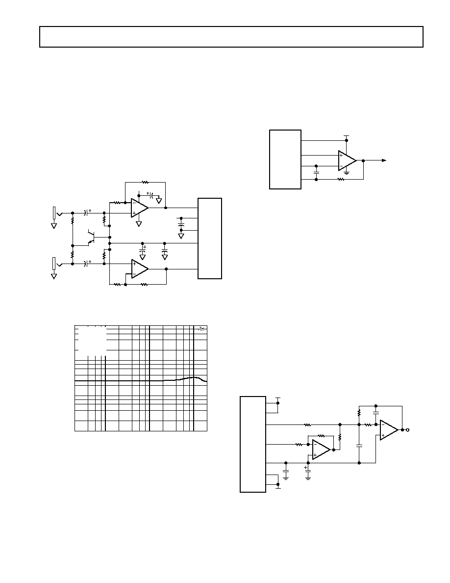
Multimedia Soundcard Microphone Preamplifier
The low distortion and low noise figures of the SSM2275 make
it an excellent device for amplifying low level audio signals. Fig-
ure 38 shows how the SSM2275 can be configured as a stereo
microphone preamplifier driving the input to a multimedia
sound codec, the AD1848. The SSM2275 can be powered from
the same +5 V single supply as the AD1848. The V
REF
pin on
the AD1848 provides a bias voltage of 2.25 V for the SSM2275.
This voltage can also be used to provide phantom power to a
condenser microphone through a 2N4124 transistor buffer and
2 k
resistors. The phantom power circuitry can be omitted for
dynamic microphones. The gain of SSM2275 amplifiers is set
by R2/R1 which is 100 (40 dB) as shown. Figure 39 shows the
device's THD+N performance with a 1 V
RMS
output.
L CHANNEL
MIC IN
10 F
4
6
5
8
7
10 F
1/2
SSM2275
10 F
+5V
1/2
SSM2275
0.1 F
1
2
3
R2
10k
R CHANNEL
MIC IN
R1
100
0.1 F
29
35/36
34/37
+5V
LMIC
V
CC
GND
V
REF
RMIC
AD1848
32
28
10k
10k
+5V
2N4124
10 F
2k
2k
R1
100
R2
10k
Figure 38. Low Noise Microphone Preamplifier for
Multimedia Soundcard Codec
FREQUENCY Hz
1
0.1
0.001
20
20k
100
THD + N %
1k
0.01
10k
A
V
= +40dB
V
SY
= ±2.5V
V
IN
= 40dBV
R
L
> 10k
B
W
= 22kHz
Figure 39. THD+N vs. Frequency (V
SY
= +5 V, A
V
= 40 dB,
V
OUT
= 1 V rms)
High Performance I-V Converters and Filters for 20-Bit DACs
Because of the increasing resolution and lower harmonic distor-
tions required by more audio applications, the need for high
quality amplifiers at the output of D/A converters becomes criti-
cal. The SSM2275 and SSM2475 can be used as current-to-
voltage converters and smoothing filters for 18- and 20-bit
DACs, achieving 0.0006% THD+N figures while running from
the same +5 V or +12 V source used to power the D/A con-
verter. Figure 40 shows how the SSM2275 can be used with the
AD1862, a current output 20-bit DAC.
The AD1862 has a built in 3 k
resistor that is connected from
the inverting input to the output of the amplifier. The full-scale
output current of the AD1862 is
±
1 mA, resulting in a maximum
output voltage of
±
3 V. Additional feedback resistance can be
added in the feedback loop to increase the output voltage. With
R
FB
connected the maximum output voltage will be:
V
mA
k
R
OUT MAX
FB
,
=
×
+
(
)
1
3
(10)
100pF
TO LPF
SSM2275-A
+12V
16
12
11
10
R
FB
(OPTIONAL)
V
CC
ACOM
I
OUT
R
F
AD1862
NOTE: ADDITIONAL PIN CONNECTIONS OMITTED FOR CLARITY
Figure 40. A High Performance I-V Converter for a 20-Bit DAC
In Figure 41, the SSM2275 is used as a low-pass filter for one
channel of the AD1855, a 24-bit 96 kHz stereo sigma-delta
DAC, which uses a complementary voltage output. The filter is
configured as a second order low-pass Bessel filter with a cutoff
frequency of 50 kHz. This provides a phase linear response from
dc to 24 kHz, which is ideal for high quality audio applications.
The SSM2275 can be connected to the same +5 V power sup-
ply source, that the AD1855 is connected to, eliminating the
need for extra power circuitry. The FILT output (Pin 14) from
the AD1855 provides a common reference voltage equal to half
of the supply voltage for the SSM2275.
Amplifier A1 is used as a unity-gain inverter for the positive out-
put of the AD1855. The output of A1 is combined with a nega-
tive output of the AD1855 into the active low pass filter around
A2. The output impedance of each output of the AD1855 is
100
which must be taken into account to achieve proper dc
gain, which in Figure 41 is unity gain. In this configuration the
SSM2275 can drive reasonable capacitive loads, making the de-
vice suitable for the RCA jack line outputs found in most con-
sumer audio equipment.
A1
1.15k
10 F
A2
10 F
1.15k
1.05k
237
4.7nF
562
1.05k
0.1 F
OUT
13 OR 18
12 OR 17
14
1
15
28
18
+5V
+5V
V
DD
V
DD
OUT
OUT+
FILT
GND
GND
AD1855
A1 AND A2 ARE SSM2275
OR 1/2 SSM2475
NOTE: ADDITIONAL PIN CONNECTIONS
OMITTED FOR CLARITY
Figure 41. Low-Pass Filter for a 24-Bit Stereo Sigma-
Delta DAC
SSM2275/SSM2475
REV. A
14
SPICE Macro-model
The SPICE macro-model for the SSM2275 is shown in Listing
1 on the following page. This model is based on typical values
for the device and can be downloaded from Analog Devices'
Internet site at www.analog.com. The model uses a common
emitter output stage to provide rail-to-rail performance. A resis-
tor and dc voltage source, in series with the collector, accurately
portray output dropout voltage versus output current. The
VCMH and VCML sources set the upper and lower limits of
the input common mode voltage range. Both are set up as a
function of the supply voltage to mimic the varying common
mode range with supply voltage. The EOS voltage source estab-
lishes the offset voltage and is also used to create the common-
mode rejection and power supply rejection characteristics for
the model.
A secondary pole section is also set up to vary the gain band-
width product and phase margin of the model based on the
supply voltage. The H1 and VR1 sources set up an equivalent
resistor that is linearly varied with supply voltage. This equiva-
lent resistance, in parallel with C2, creates the secondary pole.
G2 is also linearly varied to increase the GBW at higher supply
voltages. With a supply voltage of 5 V, the gain bandwidth
product is 6.3 MHz with a 47 degree phase margin. At a 30 V
supply voltage, the GBW product moves out to 7.5 MHz with
48
°
phase margin.
The broadband input referred voltage noise for the model is
6.8 nV/
Hz. Flicker noise characteristics are also accurately
modeled with the 1/f corner frequency set through the KF and
AF terms in the input stage transistors. Finally, a voltage-con-
trolled current source, GSY, is used to model the amplifier's
supply current versus supply voltage characteristics.
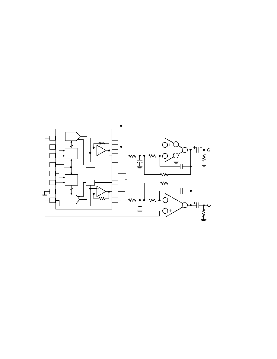
6
7
5
100pF
330pF
16
15
14
13
12
11
10
9
18-BIT
DAC
18-BIT
SERIAL
REG.
VOL
AGND
18-BIT
SERIAL
REG.
18-BIT
DAC
VOR
VBL
DGND
VBR
LR
DR
LL
DL
CK
V
L
1
2
3
4
5
6
7
8
AD1868
220 F
47k
RIGHT
CHANNEL
OUTPUT
330pF
100pF
220 F
LEFT
CHANNEL
OUTPUT
+5V SUPPLY
1
3
2
4
8
1/2
SSM2275
1/2
SSM2275
47k
7.68k
7.68k
7.68k
7.68k
9.76k
9.76k
V
REF
V
REF
V
S
Figure 42. A Smoothing Filter for an 18-Bit Stereo DAC

SSM2275/SSM2475
REV. A
15
Listing 1: SSM2275 SPICE Macro-Model
* SSM2275 SPICE Macro-Model Typical Values
* 8/97, Ver. 1
* TAM / ADSC
*
* Node assignments
*
non-inverting input
*
|
inverting input
*
|
|
positive supply
*
|
|
|
negative supply
*
|
|
|
|
output
*
|
|
|
|
|
*
|
|
|
|
|
.SUBCKT SSM2275
1
2
99
50
45
*
* INPUT STAGE
*
Q1 4 3 5 QNIX
Q2 6 2 7 QNIX
RC1 99 11 15E3
RC2 99 12 15E3
RE1 5 8 1E3
RE2 7 8 1E3
EOS 3 1 POLY(2) (61,98) (73,98) 1.5E-3 1.78E-5 1
IOS 1 2 5E-9
ECMH1 4 11 POLY(1) (99,50) 0.9 -30E-3
ECMH2 6 12 POLY(1) (99,50) 0.9 -30E-3
ECML1 9 50 POLY(1) (99,50) 0.1 30E-3
ECML2 10 50 POLY(1) (99,50) 0.1 30E-3
D1 9 5 DX
D2 10 7 DX
D3 13 1 DZ
D4 2 13 DZ
IBIAS 8 50 200E-6
*
* CMRR=115 dB, ZERO AT 1kHz, POLE AT 10kHz
*
ECM1 60 98 POLY(2) (1,98) (2,98) 0 .5 .5
RCM1 60 61 159.2E3
RCM2 61 98 17.66E3
CCM1 60 61 1E-9
*
* PSRR=120dB, ZERO AT 1kHz
*
RPS1 70 0 1E6
RPS2 71 0 1E6
CPS1 99 70 1E-5
CPS2 50 71 1E-5
EPSY 98 72 POLY(2) (70,0) (0,71) 0 1 1
RPS3 72 73 1.59E6
CPS3 72 73 1E-10
RPS4 73 98 1.59
*
* INTERNAL VOLTAGE REFERENCE
*
RSY1 99 91 100E3
RSY2 50 90 100E3
VSN1 91 90 DC 0
EREF 98 0 (90,0) 1
GSY 99 50 POLY(1) (99,50) 0.97E-3 -7E-6
*
* ADAPTIVE POLE AND GAIN STAGE
* AT Vsy= 5, fp=12.50MHz,Av=1
* AT Vsy=30, fp=18.75MHz,Av=1.16
*
G2 98 20 POLY(2) (4,6) (99,50) 0 80.3E-6 0 0 2.79E-6
VR1 20 21 DC 0
H1 21 98 POLY(2) VR1 VSN1 0 11.317E3 0 0 -28.29E6
C2 20 98 1.2E-12
*
* POLE AT 90MHz
*
G3 98 23 (20,98) 565.5E-6
R5 23 98 1.768E3
C3 23 98 1E-12
*
* GAIN STAGE
*
G1 98 30 (23,98) 733.3E-6
R1 30 98 9.993E3
CF 30 45 200E-12
D5 31 99 DX
D6 50 32 DX
V1 31 30 0.6
V2 30 32 0.6
*
* OUTPUT STAGE
*
Q3 46 42 99 QPOX
Q4 47 44 50 QNOX
RO1 46 48 30
RO2 47 49 30
VO1 45 48 15E-3
VO2 49 45 10E-3
RB1 41 42 200
RB2 43 44 200
EO1 99 41 POLY(1) (98,30) 0.7528 1
EO2 43 50 POLY(1) (30,98) 0.7528 1
*
* MODELS
*
.MODEL QNIX NPN(IS=1E-16,BF=400,KF=1.96E-14,AF=1)
.MODEL QNOX NPN(IS=1E-16,BF=100,VAF=130)
.MODEL QPOX PNP(IS=1E-16,BF=100,VAF=130)
.MODEL DX D(IS=1E-16)
.MODEL DZ D(IS=1E-14,BV=6.6)
.ENDS SSM2275
SSM2275/SSM2475
REV. A
16
C3239a04/99
PRINTED IN U.S.A.
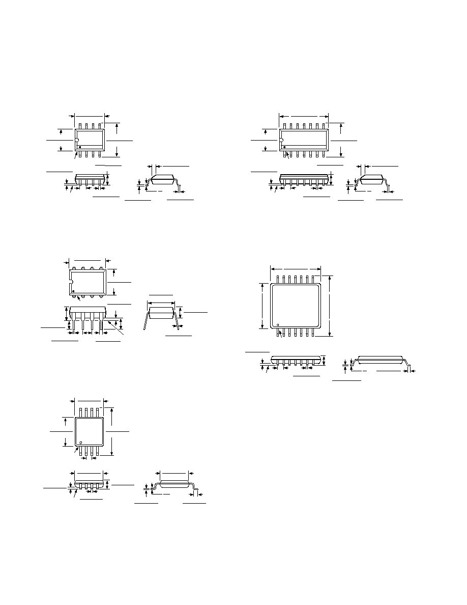
8-Lead SOIC
(SO-8)
0.1968 (5.00)
0.1890 (4.80)
8
5
4
1
0.2440 (6.20)
0.2284 (5.80)
PIN 1
0.1574 (4.00)
0.1497 (3.80)
0.0688 (1.75)
0.0532 (1.35)
SEATING
PLANE
0.0098 (0.25)
0.0040 (0.10)
0.0192 (0.49)
0.0138 (0.35)
0.0500
(1.27)
BSC
0.0098 (0.25)
0.0075 (0.19)
0.0500 (1.27)
0.0160 (0.41)
8
°
0
°
0.0196 (0.50)
0.0099 (0.25)
x 45
°
OUTLINE DIMENSIONS
Dimensions shown in inches and (mm).
14-Lead SOIC
(R-14)
14
8
7
1
0.3444 (8.75)
0.3367 (8.55)
0.2440 (6.20)
0.2284 (5.80)
0.1574 (4.00)
0.1497 (3.80)
PIN 1
SEATING
PLANE
0.0098 (0.25)
0.0040 (0.10)
0.0192 (0.49)
0.0138 (0.35)
0.0688 (1.75)
0.0532 (1.35)
0.0500
(1.27)
BSC
0.0099 (0.25)
0.0075 (0.19)
0.0500 (1.27)
0.0160 (0.41)
8
°
0
°
0.0196 (0.50)
0.0099 (0.25)
x 45
°
14-Lead TSSOP
(RU-14)
14
8
7
1
0.201 (5.10)
0.193 (4.90)
0.256 (6.50)
0.246 (6.25)
0.177 (4.50)
0.169 (4.30)
PIN 1
SEATING
PLANE
0.006 (0.15)
0.002 (0.05)
0.0118 (0.30)
0.0075 (0.19)
0.0256
(0.65)
BSC
0.0433
(1.10)
MAX
0.0079 (0.20)
0.0035 (0.090)
0.028 (0.70)
0.020 (0.50)
8
°
0
°
8-Lead Plastic DIP
(N-8)
8
1
4
5
0.430 (10.92)
0.348 (8.84)
0.280 (7.11)
0.240 (6.10)
PIN 1
SEATING
PLANE
0.022 (0.558)
0.014 (0.356)
0.060 (1.52)
0.015 (0.38)
0.210 (5.33)
MAX
0.130
(3.30)
MIN
0.070 (1.77)
0.045 (1.15)
0.100
(2.54)
BSC
0.160 (4.06)
0.115 (2.93)
0.325 (8.25)
0.300 (7.62)
0.015 (0.381)
0.008 (0.204)
0.195 (4.95)
0.115 (2.93)
8-Lead microSOIC
(RM-8)
8
5
4
1
0.122 (3.10)
0.114 (2.90)
0.199 (5.05)
0.187 (4.75)
PIN 1
0.0256 (0.65) BSC
0.122 (3.10)
0.114 (2.90)
SEATING
PLANE
0.006 (0.15)
0.002 (0.05)
0.018 (0.46)
0.008 (0.20)
0.043 (1.09)
0.037 (0.94)
0.120 (3.05)
0.112 (2.84)
0.011 (0.28)
0.003 (0.08)
0.028 (0.71)
0.016 (0.41)
33
°
27
°
0.120 (3.05)
0.112 (2.84)