 | –≠–ª–µ–∫—Ç—Ä–æ–Ω–Ω—ã–π –∫–æ–º–ø–æ–Ω–µ–Ω—Ç: SW06B | –°–∫–∞—á–∞—Ç—å:  PDF PDF  ZIP ZIP |
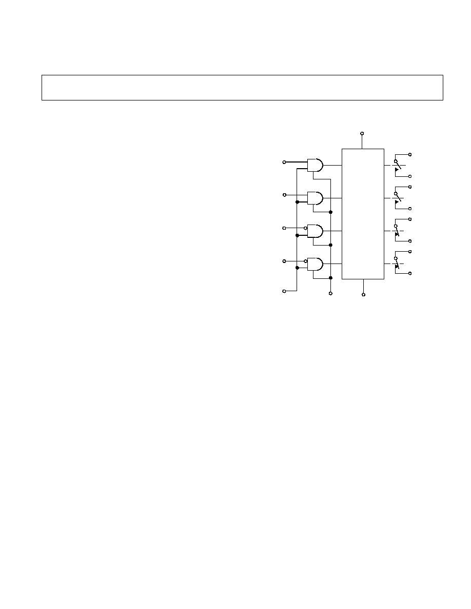
FUNCTIONAL BLOCK DIAGRAM
LEVEL
SHIFT
V+
12
V≠
5
IN 1
IN 2
IN 3
IN 4
DIS
13
16
9
8
1
4
GND
S1
D1
S2
D2
S3
D3
S4
D4
3
2
6
7
11
10
14
15
REV. A
Information furnished by Analog Devices is believed to be accurate and
reliable. However, no responsibility is assumed by Analog Devices for its
use, nor for any infringements of patents or other rights of third parties
which may result from its use. No license is granted by implication or
otherwise under any patent or patent rights of Analog Devices.
a
Quad SPST JFET
Analog Switch
SW06
One Technology Way, P.O. Box 9106, Norwood, MA 02062-9106, U.S.A.
Tel: 617/329-4700
Fax: 617/326-8703
FEATURES
Two Normally Open and Two Normally Closed SPST
Switches with Disable
Switches Can Be Easily Configured as a Dual SPDT or
a DPDT
Highly Resistant to Static Discharge Destruction
Higher Resistance to Radiation than Analog Switches
Designed with MOS Devices
Guaranteed R
ON
Matching: 10% max
Guaranteed Switching Speeds
T
ON
= 500 ns max
T
OFF
= 400 ns max
Guaranteed Break-Before-Make Switching
Low "ON" Resistance: 80 max
Low R
ON
Variation from Analog Input Voltage: 5%
Low Total Harmonic Distortion: 0.01%
Low Leakage Currents at High Temperature
T
A
= +125 C: 100 nA max
T
A
= +85 C: 30 nA max
Digital Inputs TTL/CMOS Compatible and Independent
of V+
Improved Specifications and Pin Compatible to
LF-11333/13333
Dual or Single Power Supply Operation
Available in Die Form
GENERAL DESCRIPTION
The SW06 is a four channel single-pole, single-throw analog
switch that employs both bipolar and ion-implanted FET
devices. The SW06 FET switches use bipolar digital logic inputs
which are more resistant to static electricity than CMOS devices.
Ruggedness and reliability are inherent in the SW06 design and
construction technology.
Increased reliability is complemented by excellent electrical
specifications. Potential error sources are reduced by minimizing
"ON" resistance and controlling leakage currents at high tem-
peratures. The switching FET exhibits minimal R
ON
variation
over a 20 V analog signal range and with power supply voltage
changes. Operation from a single positive power supply voltage
is possible. With V+ = 36 V, V≠ = 0 V, the analog signal range
will extend from ground to +32 V.
PNP logic inputs are TTL and CMOS compatible to allow the
SW06 to upgrade existing designs. The logic "0" and logic "1"
input currents are at microampere levels reducing loading on
CMOS and TTL logic.
REV. A
≠2≠
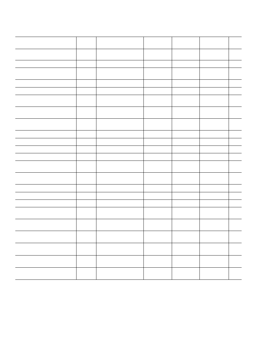
SW06≠SPECIFICATIONS
ELECTRICAL CHARACTERISTICS
SW06B
SW06F
SW06G
Parameter
Symbol
Conditions
Min Typ Max
Min Typ Max
Min Typ Max
Units
"ON" RESISTANCE
R
ON
V
S
= 0 V, I
S
= 1 mA
60
80
60
100
100
150
V
S
=
±
10 V, I
S
= 1 mA
65
80
65
100
100
150
R
ON
MATCH BETWEEN SWITCHES
R
ON
Match
V
S
= 0 V, I
S
= 100
µ
A
1
5
10
5
20
20
%
ANALOG VOLTAGE RANGE
V
A
I
S
= 1 mA
2
+10 +11
+10 +11
+10
+11
V
I
S
= 1 mA
2
≠10
≠15
≠10
≠15
≠10
≠15
ANALOG CURRENT RANGE
I
A
V
S
=
±
10 V
10
15
7
12
5
10
mA
R
ON
VS. APPLIED VOLTAGE
R
ON
≠10 V
V
S
10 V, I
S
= 1.0 mA
5
15
10
20
10
20
%
SOURCE CURRENT IN
"OFF" CONDITION
I
S(OFF)
V
S
= 10 V, V
D
= ≠10 V
3
0.3
2.0
0.3
2.0
0.3
10
nA
DRAIN CURRENT IN
"OFF" CONDITION
I
D(OFF)
V
S
= 10 V, V
D
= ≠10 V
3
0.3
2.0
0.3
2.0
0.3
10
nA
SOURCE CURRENT IN
I
S(ON)+
V
S
= V
D
=
±
10 V
3
0.3
2.0
0.3
2.0
0.3
10
nA
"ON" CONDITION
I
D(ON)
LOGICAL "1" INPUT VOLTAGE
V
INH
Full Temperature Range
2, 4
2.0
2.0
2.0
V
LOGICAL "0" INPUT VOLTAGE
V
INL
Full Temperature Range
2, 4
0.8
0.8
0.8
V
LOGICAL "1" INPUT CURRENT
I
INH
V
IN
= 2.0 V to 15.0 V
5
5
5
10
µ
A
LOGICAL "0" INPUT
I
INL
V
IN
= 0.8 V
1.5
5.0
1.5
5.0
1.5
10.0
µ
A
TURN-ON TIME
t
ON
See Switching Time
340
500
340 600
340
700
ns
Test Circuit
4, 6
TURN-OFF TIME
t
OFF
See Switching Time
200
400
200 400
200
500
ns
Test Circuit
4, 6
BREAK-BEFORE-MAKE TIME
t
ON
≠t
OFF
Note 7
50
140
50
140
50
140
ns
SOURCE CAPACITANCE
C
S(OFF)
V
S
= 0 V
3
7.0
7.0
7.0
pF
DRAIN CAPACITANCE
C
D(OFF)
V
S
= 0 V
3
5.5
5.5
5.5
pF
CHANNEL "ON" CAPACITANCE
C
D(ON)+
V
S
= V
D
= 0 V
3
15
15
15
pF
C
S(ON)
"OFF" ISOLATION
I
SO(OFF)
V
S
= 5 V rms, R
L
= 680
,
58
58
58
dB
C
L
= 7 pF, f = 500 kHz
3
CROSSTALK
C
T
V
S
= 5 V rms, R
L
= 680
,
70
70
70
dB
C
L
= 7 pF, f = 500 kHz
3
POSITIVE SUPPLY CURRENT
I+
All Channels "OFF",
5.0
6.0
5.0
9.0
6.0
9.0
mA
DIS = "0"
3
NEGATIVE SUPPLY CURRENT
I≠
All Channels "OFF",
3.0
5.0
4.0
7.0
4.0
7.0
mA
DIS = "0"
3
GROUND CURRENT
I
G
All Channels "ON" or
3.0
4.0
3.0
4.0
3.0
5.0
mA
"OFF"
3
(@ V+ = +15 V, V≠ = ≠15 V and T
A
= +25 C, unless otherwise noted)
SW06
REV. A
≠3≠
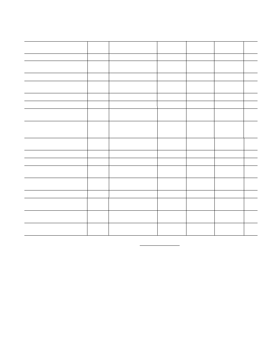
ELECTRICAL CHARACTERISTICS
SW06B
SW06F
SW06G
Parameter
Symbol
Conditions
Min Typ Max
Min Typ Max
Min Typ Max
Units
TEMPERATURE RANGE
T
A
Operating
≠55
+125
≠25
+85
0
70
∞
C
"ON" RESISTANCE
R
ON
V
S
= 0 V, I
S
= 1.0 mA
75
110
75
125
75
175
V
S
=
±
10 V, I
S
= 1.0 mA
80
110
80
125
80
175
R
ON
MATCH BETWEEN SWITCHES R
ON
Match
V
S
= 0 V, I
S
= 100
µ
A
1
6
20
6
25
10
%
ANALOG VOLTAGE RANGE
V
A
I
S
= 1.0 mA
2
+10 +11
+10 +11
+10
+11
V
I
S
= 1.0 mA
2
≠10
≠15
≠10
≠15
≠10
≠15
ANALOG CURRENT RANGE
I
A
V
S
=
±
10 V
7
12
5
11
11
mA
R
ON
WITH APPLIED VOLTAGE
R
ON
≠10 V
V
S
10 V, I
S
= 1.0 mA
10
12
15
%
SOURCE CURRENT IN
V
S
= 10 V, V
D
= ≠10 V
"OFF" CONDITION
I
S(OFF)
T
A
= Max Operating Temp
3, 9
60
30
60
nA
DRAIN CURRENT IN
V
S
= 10 V, V
D
= ≠10 V
"OFF" CONDITION
I
D(OFF)
T
A
= Max Operating Temp
3, 9
60
30
60
nA
LEAKAGE CURRENT IN
I
S(ON)+
V
S
= V
D
=
±
10 V
100
30
60
nA
"ON" CONDITION
I
D(ON)
T
A
= Max Operating Temp
3, 9
LOGICAL "1" INPUT CURRENT
I
INH
V
IN
= 2.0 V to 15.0 V
5
10
10
15
µ
A
LOGICAL "0" INPUT CURRENT
I
INL
V
IN
= 0.8 V
4
10
4
10
5
15
µ
A
TURN-ON TIME
t
ON
See Switching Time
440
900
500 900
1000
ns
Test Circuit
4, 8
TURN-OFF TIME
t
OFF
See Switching Time
300
500
330 500
500
ns
Test Circuit
4, 8
BREAK-BEFORE-MAKE TIME
t
ON
≠t
OFF
Note 7
70
70
50
ns
POSITIVE SUPPLY CURRENT
I+
All Channels "OFF,"
9.0
13.5
13.5
mA
DIS = "0"
3
NEGATIVE SUPPLY CURRENT
I≠
All Channels "OFF,"
7.5
10.5
10.5
mA
DIS = "0"
3
GROUND CURRENT
I
G
All Channels "ON" or
6.0
7.5
7.5
mA
"OFF"
3
NOTES
(@ V+ = +15 V, V≠ = ≠15 V, ≠55 C
T
A
+125 C for SW06BQ, ≠40 C
T
A
+85 C for
SW06FQ and ≠40 C
T
A
+85 C for SW06GP/GS, unless otherwise noted)
1
V
S
= 0 V, I
S
= 100
µ
A. Specified as a percentage of R
AVERAGE
where: R
AVERAGE
=
R
ON1
+
R
ON 2
+
R
ON 3
+
R
ON 4
4
.
2
Guaranteed by R
ON
and leakage tests. For normal operation maximum analog signal voltages should be restricted to less than (V+) ≠4 V.
3
Switch being tested ON or OFF as indicated, V
INH
= 2.0 V or V
INL
= 0.8 V, per logic truth table.
4
Also applies to disable pin.
5
Current tested at V
IN
= 2.0 V. This is worst case condition.
6
Sample tested.
7
Switch is guaranteed by design to provide break-before-make operation.
8
Guaranteed by design.
9
Parameter tested only at T
A
= +125
∞
C for military grade device.
Specifications subject to change without notice.
SW06
REV. A
≠4≠
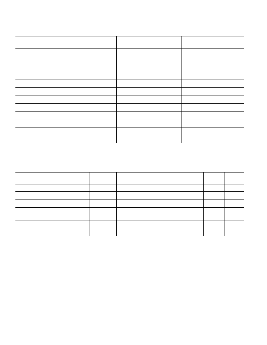
WAFER TEST LIMITS
SW06N
SW06G
Parameter
Symbol
Conditions
Limit
Limit
Units
"ON" RESISTANCE
R
ON
≠10 V
V
A
10 V, I
S
1 mA
80
100
max
R
ON
MATCH BETWEEN SWITCHES
R
ON
Match
V
A
= 0 V, I
S
100
µ
A
15
20
% max
R
ON
VS. V
A
R
ON
≠10 V
V
A
10 V, I
S
1 mA
10
20
% max
POSITIVE SUPPLY CURRENT
I+
Note 1
6.0
9.0
mA max
NEGATIVE SUPPLY CURRENT
I≠
Note 1
5.0
7.0
mA max
GROUND CURRENT
I
G
Note 1
4.0
4.0
mA max
ANALOG VOLTAGE RANGE
V
A
I
S
= 1 mA
±
10.0
±
10.0
V min
LOGIC "1" INPUT VOLTAGE
V
INH
Note 2
2.0
2.0
V min
LOGIC "0" INPUT VOLTAGE
V
INL
Note 2
0.8
0.8
V max
LOGIC "0" INPUT CURRENT
I
INL
0 V
V
IN
0.8 V
5.0
5.0
µ
A max
LOGIC "1" INPUT CURRENT
I
INH
2.0 V
V
IN
15 V
3
5
5
µ
A max
ANALOG CURRENT RANGE
I
A
V
S
=
±
10 mV
10
7
mA min
NOTE
Electrical tests are performed at wafer probe to the limits shown. Due to variations in assembly methods and normal yield loss, yield after packaging is not guaranteed
for standard product dice. Consult factory to negotiate specifications based on dice lot qualification through sample lot assembly and testing.
TYPICAL ELECTRICAL CHARACTERISTICS
SW06N
SW06G
Parameter
Symbol
Conditions
Typical
Typical
Units
"ON" RESISTANCE
R
ON
≠10 V
V
A
10 V, I
S
1 mA
60
60
TURN-ON TIME
t
ON
340
340
ns
TURN-OFF TIME
t
OFF
200
200
ns
DRAIN CURRENT IN
"OFF" CONDITION
I
D(OFF)
V
S
= 10 V, V
D
= ≠10 V
0.3
0.3
nA
"OFF" ISOLATION
I
SO(OFF)
f = 500 kHz, R
L
= 680
58
58
dB
CROSSTALK
C
T
f = 500 kHz, R
L
= 680
70
70
dB
NOTES
1
Power supply and ground current specified for switch "ON" or "OFF."
2
Guaranteed by R
ON
and leakage tests.
3
Current tested at V
IN
= 2.0 V. This is worst case condition.
(@ V+ = +15 V, V≠ = ≠15 V, T
A
= +25 C, unless otherwise noted)
(@ V+ = +15 V, V≠ = ≠15 V, T
A
= +25 C, unless otherwise noted)

SW06
REV. A
≠5≠
ORDERING GUIDE
Temperature
Package
Package
Model
Range
Description
Option
SW06BQ
≠55
∞
C to +125
∞
C
Cerdip
Q-16
SW06BRC
≠55
∞
C to +125
∞
C
LCC
E-20A
SW06FQ
≠40
∞
C to +85
∞
C
Cerdip
Q-16
SW06GP
≠40
∞
C to +85
∞
C
Plastic DIP
N-16
SW06GS
≠40
∞
C to +85
∞
C
SOL
R-16
TRUTH TABLE
Switch State
Disable
Logic
Channels
Channels
Input
Input
1 & 2
3 & 4
0
X
OFF
OFF
1 or NC
0
OFF
ON
1 or NC
1
ON
OFF
ABSOLUTE MAXIMUM RATINGS
1
Operating Temperature Range
SW06BQ, BRC . . . . . . . . . . . . . . . . . . . ≠55
∞
C to +125
∞
C
SW06FQ . . . . . . . . . . . . . . . . . . . . . . . . . ≠40
∞
C to +85
∞
C
SW06GP, GS . . . . . . . . . . . . . . . . . . . . . . ≠40
∞
C to +85
∞
C
Storage Temperature Range . . . . . . . . . . . ≠65
∞
C to +150
∞
C
Lead Temperature (Soldering, 60 sec) . . . . . . . . . . . . +300
∞
C
Maximum Junction Temperature . . . . . . . . . . . . . . . . +150
∞
C
V+ Supply to V≠ Supply . . . . . . . . . . . . . . . . . . . . . . . +36 V
V+ Supply to Ground . . . . . . . . . . . . . . . . . . . . . . . . . +36 V
Logic Input Voltage . . . . . . . . . . . (≠4 V or V≠) to V+ Supply
Analog Input Voltage Range
Continuous . . . . . . . . . . . . . V≠ Supply to V+ Supply +20 V
Maximum Current Through
Any Pin Including Switch . . . . . . . . . . . . . . . . . . . . . 30 mA
Package Type
JA
2
JC
Units
16-Pin Hermetic DIP (Q)
100
16
∞
C/W
16-Pin Plastic DIP (P)
82
39
∞
C/W
20-Contact LCC (RC)
98
38
∞
C/W
16-Pin SOL (S)
98
30
∞
C/W
NOTES
1
Absolute maximum ratings apply to both DICE and packaged parts, unless
otherwise noted.
2
JA
is specified for worst case mounting conditions, i.e.,
JA
is specified for device
in socket for Cerdip, P-DIP, and LCC packages;
JA
is specified for device soldered
to printed circuit board for SO package.
DICE CHARACTERISTICS
Die Size 0.101
◊
0.097 inch, 9797 sq. mils
(2.565
◊
2.464 mm, 6320 sq. mm)
PIN CONNECTIONS
16-Pin DIP (Q or P-Suffix)
16-Pin SOL (S-Suffix)
SW06BRC/883
LCC Package
(RC-Suffix)