Advanced Monolithic Systems, Inc. 6680B Sierra Lane, Dublin, CA 94568 Phone (925) 556-9090 Fax (925) 556-9140
Advanced
AMS112
Monolithic
150mA LOW DROPOUT VOLTAGE REGULATOR
Systems
WITH ON/OFF SWITCH
PRELIMINARY INFORMATION
FEATURES
APPLICATIONS
∑
∑
3.3V and 5V Voltage Available*
∑
∑
Battery Powered Systems
∑
∑
Active High On/Off Control
∑
∑
Portable Consumer Equipment
∑
∑
Output Current of 150mA
∑
∑
Cordless Telephones
∑
∑
Very Low Quiescent Current
∑
∑
Portable (Notebook) Computers
∑
∑
Low Dropout Voltage of 80mV at 30mA
∑
∑
Portable Instrumentation
∑
∑
Very Low Noise
∑
∑
Radio Control Systems
∑
∑
Short Circuit Protection
∑
∑
Personal Communication Equipment
∑
∑
Internal Thermal Shutdown
∑
∑
Toys
∑
∑
Space Saving 5 Lead SOT-23 Package
∑
∑
Low Voltage Systems
GENERAL DESCRIPTION
The AMS112 series consists of positive fixed voltage regulators featuring an internal electronic switch controlled by TTL or
CMOS logic levels. When the Control pin is pulled to a logic high level, the device is in the ON state. If the control function
is not used, the control terminal should be connected to a logic high level or V
IN
, therefore allowing the regulator to be ON.
The regulator will be ON when the control terminal voltage is grater than 1.8V. To lower the output noise level to 30
µ
V
rms
,
an external capacitor can be connected to the noise bypass pin. These devices feature very low quiescent current of 1mA when
supplying 30mA loads (180
µ
A at no load). This unique characteristic and the low standby current (typ. 100nA) make the
AMS112 ideal to use for standby power systems. Like other regulators the AMS112 series also includes internal current
limiting and thermal shutdown.
The AMS112 is offered in 3.3V and 5.0V output voltages, and is available in the 5-pin SOT-23 surface mount package.
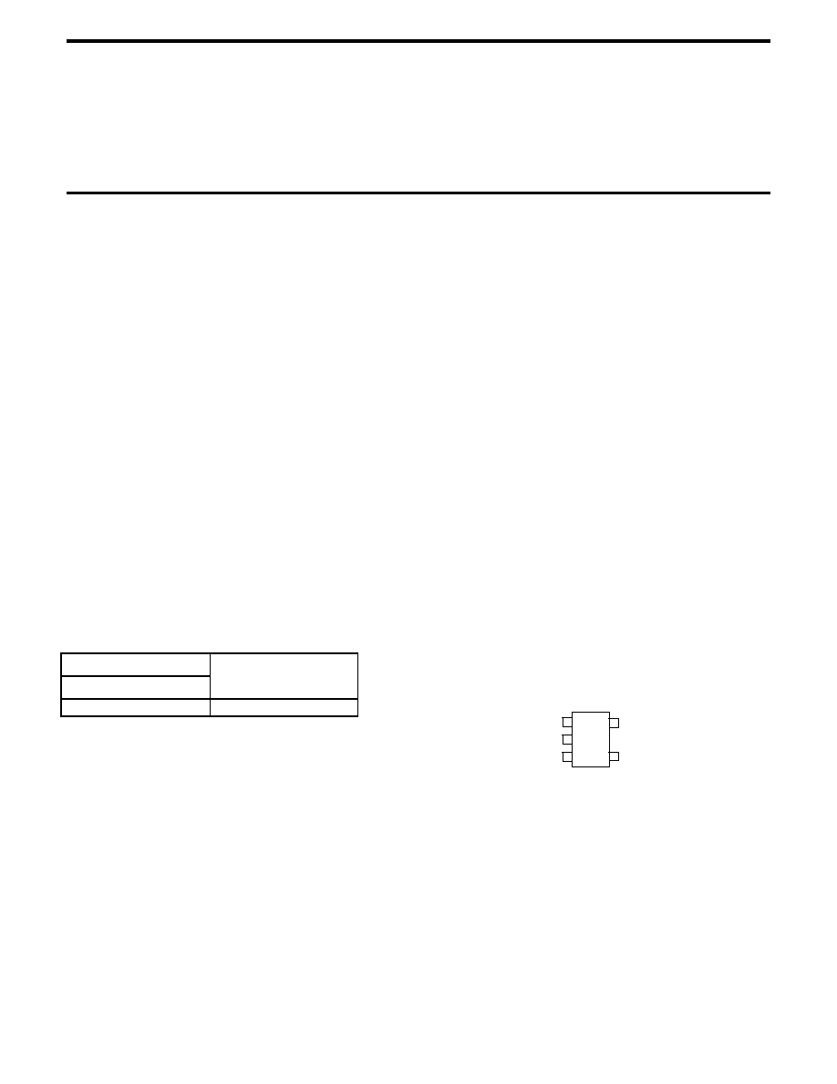
ORDERING INFORMATION
PIN CONNECTIONS
PACKAGE TYPE
OPERATING TEMP.
5L SOT-23
RANGE
AMS112M1-X
IND
X =3.3V or 5V
*For additional available fixed voltages contact factory
5 Lead SOT-23
(M1)
ON/OFF
INPUT
BYPASS
OUTPUT
GROUND
1
2
5
3
4
Bottom View

Advanced Monolithic Systems, Inc. 6680B Sierra Lane, Dublin, CA 94568 Phone (925) 556-9090 Fax (925) 556-9140
AMS112
ABSOLUTE MAXIMUM RATINGS
(Note 1)
Input Voltage
16V
Maximum Junction Temperature
+150
∞
C
Power Dissipation
400mW
Storage Temperature
-55
∞
C to +150
∞
C
Operating Temperature Range
-30
∞
C to +80
∞
C
Lead Temperature (Soldering 10 sec)
230
∞
C
ELECTRICAL CHARACTERISTICS
Electrical Characteristics at T
A
=25∞C, V
IN
=V
OUT
+1V, C
P
= 0.1
µ
F unless otherwise noted.
PARAMETER
CONDITIONS
(Note 2)
Min.
AMS112-X
Typ.
Max.
Units
Output Voltage
V
IN
= V
OUT
+1V
-3
+3
%
Quiescent Current
I
O
= 0 mA, Except I
CONT
170
350
µ
A
Standby Current
V
IN
= 8V, at output off
0.1
µ
A
Line Regulation
V
IN
= V
OUT
+1V to V
OUT
+6V
3
20
mV
Load Regulation
5mA
I
O
60 mA
10
50
mV
Dropout Voltage
I
O
= 60 mA
I
O
= 150 mA
160
290
260
400
mV
mV
Output Current
180
240
mA
Ripple Rejection
100mV
rms
, I
O
=10mA
55
dB
Output Noise Voltage
10Hz < f < 80kHz, I
O
=30mA
30
µ
Vrms
Temperature Coefficient
I
O
=10mA, -20
∞
C
T
A
+75
∞
C
0.2
mV/
∞
C
Noise Bypass Terminal Voltage
1.25
V
Control Terminal Specifications
On/Off Current
Output On
12
30
µ
A
On/Off Voltage
Output On
Output Off
1.8
0.6
V
V
Output Rise Time
I
O
= 30 mA, V
CONT
= 0V to 1.8V
0.3
ms
Note 1: Absolute Maximum Ratings are limits beyond which damage to the device may occur. For guaranteed performance limits and associated test conditions, see
the Electrical Characteristics tables.
Note 2: To ensure constant junction temperature, low duty cycle pulse testing is used.

Advanced Monolithic Systems, Inc. 6680B Sierra Lane, Dublin, CA 94568 Phone (925) 556-9090 Fax (925) 556-9140
AMS112
APPLICATION HINTS
Package Power Dissipation
The package power dissipation is the level at which the thermal
sensor monitoring the junction temperature is activated. The
AMS112 shuts down when the junction temperature exceeds the
limit of 150
∞
C. The junction temperature rises as the difference
between the input power and output power increases. The
mounting pad configuration on the PCB, the board material, as
well as the ambient temperature affect the rate of temperature
rise. The junction temperature will be low, even if the power
dissipation is high, when the mounting of the device has good
thermal conductivity. When mounted on the recommended
mounting pad the power dissipation for the SOT-23 package is
400mW. For operation above 25
∞
C derate the power dissipation
at 3.2 mW/
∞
C. To determine the power dissipation for shutdown
when mounted, attach the device on the PCB and increase the
input-to-output voltage until the thermal protection circuit is
activated. Calculate the power dissipation of the device by
subtracting the output voltage from the input voltage and multiply
by the output current. The measurements should allow for the
ambient temperature of the PCB. The value obtained from P
D
/
(150
∞
C - T
A
) is the derating factor. The PCB mounting pad
should provide maximum thermal conductivity in order to
maintain low device temperatures. As a general rule, the lower
the temperature, the better the reliability of the device.
The thermal resistance when the device is mounted is equal to:
T
J
=
JA
x P
D
+ T
A
The internal limit for junction temperature is 150
∞
C. If the
ambient temperature is 25
∞
C, then:
150
∞
C =
JA
x P
D
+ 25
∞
C
JA
= 125
∞
C/ P
D
A simple way to determine P
D
is to calculate V
IN
x I
IN
when the
output is shorted. As the temperature rises, the input gradually
will decrease. The P
D
value obtained when the thermal
equilibrium is reached, is the value that should be used.
The range of usable currents can be found from the graph in
figure 2.
4
5
75
150
25
50
6
3
P
D
D
PD
T (∞C)
(mW)
Figure 2
Procedure:
1.
Find P
D
.
2.
P
D1
is calculated as P
D
x (0.8 - 0.9).
3.
Plot P
D1
against 25
∞
C.
4.
Connect P
D1
to the point corresponding to the 150
∞
C.
5.
Take a vertical line from the maximum operating
temperature (75
∞
C) to the derating curve.
6.
Read the value of P
D
at the point where the vertical line
intersects the derating curve. This is the maximum power
dissipation, D
PD
.
The maximum operating current is:
I
OUT
= (D
PD
/ (V
IN(MAX)
- V
O
)
External Capacitors
The AMS112 series require input and output decoupling
capacitors. The required value of these capacitors depends on the
application circuit and other factors.
Because high frequency characteristics of electrolytic capacitors
depend greatly on the type and even the manufacturer, the value
of capacitance that works well with AMS112 for one brand or
type may not necessary be sufficient with an electrolytic of
different origin. Sometimes actual bench testing will be the only
means to determine the proper capacitor type and value. To
obtain stability in all general applications a high quality 4.7
µ
F
aluminum electrolytic or a 2.2
µ
F tantalum electrolytic can be
used.
A critical characteristic of the electrolytic capacitors is their
performance over temperature. The AMS112 is designed to
operate to -30
∞
C, but some electrolytics will freeze around -30
∞
C
therefore becoming ineffective. In such case the result is
oscillation at the regulator output. For all application circuits
where cold operation is necessary, the output capacitor must be
rated to operate at the minimum temperature.
In order to determine the minimum value of the output capacitor,
for an application circuit, the entire circuit including the capacitor
should be bench tested at minimum operating temperatures and
maximum operating currents. After the minimum capacitance
value has been found, the value should be doubled for actual use
to cover for production variations both in the regulator and the
capacitor. The recommended minimum capacitance for AMS112
is 2.2
µ
F. As a general rule, with higher output voltages the value
of the output capacitance decreases, since the internal loop gain
is reduced.
Noise Bypass Capacitor
The noise bypass capacitor should be connected as close as
possible to pin 3 and ground. The recommended value for this
capacitor is 0.01
µ
F. The noise bypass terminal is susceptible to
external noise, and oscillation can occur when the bypass
capacitor is not used and the solder pad for this pin is too large.
Because of the high impedance of the noise bypass terminal, care
should be taken if the bypass capacitor is not used.
