 | –≠–ª–µ–∫—Ç—Ä–æ–Ω–Ω—ã–π –∫–æ–º–ø–æ–Ω–µ–Ω—Ç: AMS2026P | –°–∫–∞—á–∞—Ç—å:  PDF PDF  ZIP ZIP |
Advanced Monolithic Systems, Inc. 6680B Sierra Lane, Dublin, CA 94568 Phone (925) 556-9090 Fax (925) 556-9140
Advanced
AMS2026
Monolithic
DUAL POWER DISTRIBUTION SWITCH
Systems
FEATURES
∑
∑
110m
Typ. (5V Input) High Side MOSFET Switch
∑
∑
100
µ
µ
A Maximum On-State Supply Current
∑
∑
Short Circuit Protection
∑
∑
Available Active-High or Active-Low Enable
∑
∑
Overcurrent Protection
∑
∑
Available in Space Saving 8 lead SOIC and 8 lead PDIP
∑
∑
Thermal Protection
∑
∑
Enable Input Compatible With 3V and 5V Logic
APPLICATIONS
∑
∑
Controlled Rise and Fall Times Limit Current
∑
∑
USB Power Management
Surges and Minimize EMI
∑
∑
Hot Plug-In Power Supplies
∑
∑
Undervoltage Lock-Out Guarantees the Switch is
∑
∑
Battery-Charger Circuits
Off At Start-up
PRODUCT DESCRIPTION
The AMS2026 is a dual power distribution switch intended for applications where heavy capacitive loads and short-circuits
are likely to be encountered. The high-side switch is a 110m
N-channel MOSFET. The switch is controlled by a logic
enable input compatible with 3V and 5V logic and is available in active-high or active-low enable. The internal charge pump,
designed to control the power switch rise and fall time to minimize current surges during switching, also provides the gate
drive. Requiring no external components the charge pump allows operation from supplies as low as 3.3V. When an overload
or a short circuit is encountered the AMS2026 limits the output current to a safe level by switching into a constant-current
mode and the overcurrent logic output error flag is set to a low. Continuous heavy overloads and short circuits will increase
the power dissipation in the switch; this will cause the junction temperature to rise. The thermal protection circuit shuts the
power switch off to prevent damage. Once the device has cooled sufficiently, it will turn on automatic. An under voltage
lock-out is provided to insure that the power switch is in the Off state at start-up.
The AMS2026 is offered in the 8 lead SOIC package and the 8 lead PDIP package.
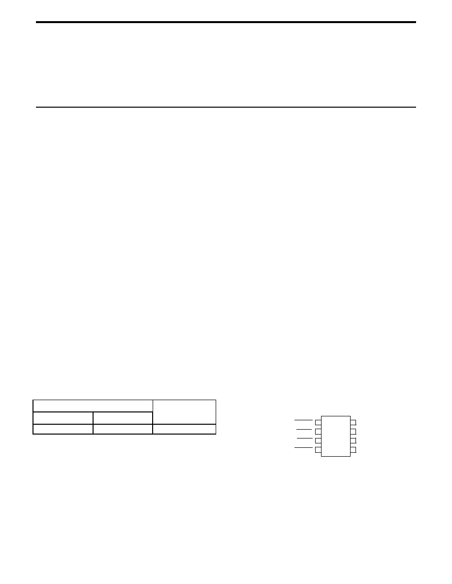
ORDERING INFORMATION
PIN CONNECTIONS
PACKAGE TYPE
OPER. TEMP
8 LEAD SOIC
8 LEAD PDIP
RANGE
AMS2026S
AMS2026P
-40
∞
C to 85
∞
C
8 LEAD SOIC/ 8 LEAD PDIP
1
2
8
4
3
7
5
6
GROUND
OUTPUT
INPUT
ENABLE
ERROR
OUTPUT
ENABLE
ERROR
Top View

Advanced Monolithic Systems, Inc. 6680B Sierra Lane, Dublin, CA 94568 Phone (925) 556-9090 Fax (925) 556-9140
AMS2026
ABSOLUTE MAXIMUM RATINGS
(Note 1)
Input Voltage Range, V
I
-0.3V to 7V
Internal Power Dissipation
(Note 3)
Output Voltage Range, V
O
-0.3V to V
I(IN)
+0.3V
Maximum Junction Temperature
+125
∞
C
Input Voltage Range, V
I
at /EN
-0.3V to 7V
Storage Temperature
-65
∞
C to +150
∞
C
Continuos Output Current, I
O
Internally Limited
Lead Temperature (Soldering 10 sec)
260
∞
C
ELECTRICAL CHARACTERISTICS
Electrical Characteristics for each section at T
J
=25∞C, V
I(IN)
= 5.5V, I
O
=rated current, /EN = 0V unless otherwise specified.
PARAMETER
CONDITIONS
(Note 2)
Min.
AMS2026
Typ.
Max.
Units
Switch On-State Resistance
V
I(IN)
= 5.5V
110
140
m
V
I(IN)
= 5.0V
110
140
m
V
I(IN)
= 4.5V
110
140
m
V
I(IN)
= 4.0V
110
140
m
Switch Output Leakage Current
/EN = V
I
0.01
5
µ
A
/EN = V
I
, -40
∞
C
T
J
85
∞
C
10
µ
A
Switch Output Rise Time
V
I(IN)
= 5.5V, C
L
= 1
µ
F
4.0
ms
V
I(IN)
= 2.7V, C
L
= 1
µ
F
3.8
ms
Switch Output Fall Time
V
I(IN)
= 5.5V, C
L
= 1
µ
F
3.9
ms
V
I(IN)
= 2.7V, C
L
= 1
µ
F
3.5
ms
Enable High-Level Input Voltage
4.0V
V
I
5.5V
2.4
V
Enable Low-Level Input Voltage
4.0V
V
I
5.5V
0.6
V
Enable Input Current
/EN = 0V or /EN = V
I
-1
1
µ
A
Enable Delay Time, Low-to-High
Output
C
L
= 1
µ
F
C
L
= 1
µ
F
20
40
ms
ms
Short Circuit Current
V
I(IN)
= 5.5V, T
J
=25∞C
OUT Connected to GND, device enable into
short circuit
0.66
1.2
1.8
A
Supply Current, Low-Level
Output
/EN = V
I
, T
J
=25∞C
/EN = V
I
, -40
∞
C
T
J
85
∞
C
0.015
10
10
µ
A
µ
A
Supply Current, High-Level
Output
/EN = 0V, T
J
=25∞C
/EN = 0V, -40
∞
C
T
J
85
∞
C
73
100
100
µ
A
µ
A
Undervoltage lock-out Low-Level
Input Voltage
2.0
3.0
3.2
V
Note 1: Absolute Maximum Ratings are limits beyond which damage to the device may occur. For guaranteed performance limits and associated test conditions, see
the Electrical Characteristics tables.
Note 2: To ensure constant junction temperature, low duty cycle pulse testing is used; thermal effects must be taken in consideration separately.
Note 3: The Power Dissipation for the SO-8 package is 725mW at T
A
= 25 ∞C. Above T
A
= 25 ∞C the Power Dissipation must be derated at 5.8mW/ ∞C (for T
A
=
70 ∞C P
D
= 464mW ; for T
A
= 125 ∞C P
D
= 145mW)
RECOMMENDED OPERATING CONDITIONS:
Min
Max
Input Voltage, V
I
4.0V
5.5V
Input Voltage, V
I
at /EN
0V
5.5V
Continuous Output Current, I
O
0A
0.6A
Operating Junction Temp. Range
-40∞C
+125∞C

Advanced Monolithic Systems, Inc. 6680B Sierra Lane, Dublin, CA 94568 Phone (925) 556-9090 Fax (925) 556-9140
AMS2026
PIN FUNCTIONS
Pin Name
Pin No.
I / O
Description
Enable
/EN (A/B)
1/4
I
Enable Input, Logic turns power switch on.
Ground
GND
6
I
Ground.
Input
IN
7
I
Power switch input, also supplies IC's internal circuitry.
Error Flag
ERROR (A/B)
2/3
O
Overcurrent, Over temperature, Logic output.
Output
OUT(A/B)
6-8
O
Power switch output.
BLOCK DIAGRAM
THERMAL
SENSE
IN
1.2V
REFERENCE
CHARGE
PUMP
UVLO
*
CS
GATE
DRIVER
CURRENT
LIMIT
POWER SWITCH
OUT A
ERROR
FLAG
CHARGE
PUMP
UVLO
*
CS
GATE
DRIVER
CURRENT
LIMIT
POWER SWITCH
OUT B
ERROR
FLAG
ENABLE A
ENABLE B
ERROR A
GND
ERROR B
*Current Sense
FUNCTIONAL DESCRIPTION
Power Switch
The power switch is an N-channel MOSFET with a maximum on-
state resistance of 140m
(V
I(IN
) = 5.0V, configured as a high-
side switch.
Charge Pump
An internal 100kHz charge pump supplies the power to the driver
circuit and provides the required voltage to pull the gate of the
MOSFET above the source. The charge pump requires very little
supply current and operates from input voltages as low as 3.0V.
Gate Driver
The driver controls the gate voltage of the power switch. The
driver incorporates circuitry that controls the rise and fall times of
the output voltage, as a result it limits large current surges and
reduces the associated electromagnetic interference (EMI)
produced. The rise and fall times of the output voltage are
typically in the 2ms to 4ms range instead of the microsecond or
nanosecond range for a standard FET.
Enable
A logic high on the /EN input turns off the power switch and the
bias for the charge pump, driver, and other circuitry to reduce the
supply current to less than 10
µ
A. A logic zero input restore bias
to the drive and control circuits and turns the power on. The
enable input is compatible with both TTL and CMOS logic
levels.
Error Flag
The error flag output, is an open drain logic output that is active
low when output current exceeds current limit. Until the fault
condition is removed the output will remain active low.
Current Limit
A sense FET monitors the current supplied to the load. In case of
an overload or short circuit, the current limit circuitry sends a
signal to the driver. The driver will then reduce the gate voltage
and drive the power FET into its linear region, which switches
the output into a constant current mode and holds the current
constant while varying the voltage on the load.
Thermal Shutdown
The internal thermal shutdown circuit will shut the power switch
off when the junction temperature rises to approx. 180∞C.
Hysteresis is build into the thermal sense circuitry, and after the
junction temperature has dropped about 20∞C, the switch turns
back on. Until the fault is removed the switch will continue to
cycle off and on.
Undervoltage Lock-out
An internal voltage sense monitors the input voltage. When the
input voltage is below 3.2V nominal, the switch is turned off by a
control signal. The typical fall time range due to the sense of a
low voltage is 250
µ
s to 750
µ
s.
Advanced Monolithic Systems, Inc. 6680B Sierra Lane, Dublin, CA 94568 Phone (925) 556-9090 Fax (925) 556-9140
AMS2026
APPLICATION HINTS
Power Supply Considerations
A 0.047
µ
F ceramic bypass capacitor close to the device, between
input and ground is recommended. When the output load is heavy
or has large paralleled capacitors, a high value electrolytic
capacitor should be used. To improve the immunity of the device to
ESD, use a 0.1
µ
F ceramic capacitor to bypass the output.
Current Limit
A sense FET monitors overcurrent conditions. When an
overcurrent condition is detected the device maintains a constant
output current and decreases the voltage accordingly. If the
condition is present long enough to activate the thermal limiting
the result is the shutdown of the device.
There are three situation in which overload can occur. In the first
case, the output has been shorted before the device is enabled or
before V
I
has been applied. The device senses the short and
switches into a constant-current output.
In the second case, the short occurs while the device is enabled.
When this happens, very high currents flow for a short time before
the current-limit circuit can react. After the current-limit circuit
has tripped, the device limits normally.
In the third case, the load has been gradually increased beyond the
recommended operating current. The current will rise until the
current-limit threshold is reached. The AMS2026 is able to deliver
current up to the current-limit threshold without damage. When the
threshold has been reached the device switches into the constant
current mode. When over current condition is detected the error
flag logic output remains low until the condition is removed.
Power Dissipation and Junction Temperature
The thermal resistance of the surface-mount packages such as
SOIC is high compared to that of power packages. The use of the
N-cannel MOSFET which has low on-resistance, makes it possible
for small surface-mount packages to pass large currents. To
determine the power dissipation and junction temperature the first
step is to find r
ON
at the input voltage and operating temperature.
As an initial estimate use the highest operating ambient
temperature of interest and read r
ON
from Figure 1. Power
dissipation is equal to:
P
D
= r
ON
x I
2
Calculate the junction temperature:
T
J
= P
D
x R
JA
+ T
A
Where R
JA
is the thermal resistance and is 172
∞
C/W for the
SOIC package. Compare the calculated junction temperature
with the initial estimate and if they don't mach within a few
degrees, repeat the calculations using the calculated value as the
new estimate. A few repetitions will be sufficient to give a
reasonable answer.
Thermal Protection
Thermal protection prevents damage to the device when over
load or short circuits conditions are present for extended periods
of time. These conditions force the AMS2026 into the constant
current mode. As a result the voltage across the high-side switch
will increase. Under short-circuit conditions the voltage across
the switch is equal to the input voltage. Continuous short
circuits and heavy over loads increase the power dissipation in
the switch and causes the junction temperature to rise to
dangerously high levels. The protection circuit shuts off the
switch when it senses the high junction temperature. The switch
remains off until the device has cooled about 20
∞
C. The switch
continues to cycle off and on until the fault is removed.
Undervoltage Lock-out
An undervoltage lock-out is provided to insure that the switch is
in the off state at start-up. When the input voltage falls below
3.0V the switch will be turned off immediately. This will make
it easy for designers of hot plug-in systems that may not be able
to turn the switch off before removing the input power. In such
cases when the device is reinserted, the turn on will have a
controlled rise time to reduce EMI and voltage overshoots.
POWER SUPPLY
4.0V - 5.0V
EXTERNAL LOAD A
0.1
µ
F
0.1
µ
F
1
µ
F
10k
2
3
6
ERROR FLAG A
ENABLE A
10k
EXTERNAL LOAD B
0.1
µ
F
1
4
ENABLE B
ERROR FLAG B
7
8
5
IN
OUT A
OUT B
EN
EN
GND
ERROR A
ERROR B
Figure 1
TYPICAL APPLICATIONS

Advanced Monolithic Systems, Inc. 6680B Sierra Lane, Dublin, CA 94568 Phone (925) 556-9090 Fax (925) 556-9140
AMS2026
PACKAGE DIMENSIONS inches (millimeters) unless otherwise noted.
8 LEAD SOIC PLASTIC PACKAGE (S)
8 LEAD PLASTIC DIP PACKAGE (P)
0∞-8∞ TYP
0.010-0.020
(0.254-0.508)
S (SO-8 ) AMS DRW# 042293
x 45∞
0.016-0.050
(0.406-1.270)
0.008-0.010
(0.203-0.254)
0.004-0.010
(0.101-0.254)
0.014-0.019
(0.355-0.483)
0.053-0.069
(1.346-1.752)
0.050
(1.270)
TYP
0.150-0.157**
(3.810-3.988)
0.228-0.244
(5.791-6.197)
0.189-0.197*
(4.801-5.004)
*DIMENSION DOES NOT INCLUDE MOLD FLASH. MOLD FLASH
SHALL NOT EXCEED 0.006" (0.152mm) PER SIDE
**DIMENSION DOES NOT INCLUDE INTERLEAD FLASH. INTERLEAD
FLASH SHALL NOT EXCEED 0.010" (0.254mm) PER SIDE
1
2
3
4
8
7
6
5
0.045-0.065
(1.143-1.651)
0.255±0.015*
(6.477±0.381)
0.400*
(10.160)
MAX
1
2
3
4
8
7
6
5
0.130±0.005
(3.302±0.127)
0.018±0.003
(0.457±0.076)
0.100±0.010
(2.540±0.254)
(
8.255
)
+0.635
-0.381
0.325 +0.025
-0.015
0.009-0.015
(0.229-0.381)
0.300-0.325
(7.620-8.255)
0.065
(1.651)
TYP
0.005
(0.127)
MIN
0.125
(3.175)
MIN
0.015
(0.380)
MIN
*DIMENSIONS DO NOT INCLUDE MOLD FLASH OR PROTUSIONS.
MOLD FLASH OR PROTUSIONS SHALL NOT EXCEED 0.010" (0.254mm)
P (8L PDIP ) AMS DRW# 042294