050-6266 Rev B 12-2005
APT15GT120BR(G)
TYPICAL PERFORMANCE CURVES
MAXIMUM RATINGS
All Ratings: T
C
= 25∞C unless otherwise specified.
STATIC ELECTRICAL CHARACTERISTICS
Characteristic / Test Conditions
Collector-Emitter Breakdown Voltage (V
GE
= 0V, I
C
= 1mA)
Gate Threshold Voltage (V
CE
= V
GE
, I
C
= 0.6mA, T
j
= 25∞C)
Collector-Emitter On Voltage (V
GE
= 15V, I
C
= 15A, T
j
= 25∞C)
Collector-Emitter On Voltage (V
GE
= 15V, I
C
= 15A, T
j
= 125∞C)
Collector Cut-off Current (V
CE
= 1200V, V
GE
= 0V, T
j
= 25∞C)
2
Collector Cut-off Current (V
CE
= 1200V, V
GE
= 0V, T
j
= 125∞C)
2
Gate-Emitter Leakage Current (V
GE
= ±20V)
Symbol
V
(BR)CES
V
GE(TH)
V
CE(ON)
I
CES
I
GES
Units
Volts
µA
nA
Symbol
V
CES
V
GE
I
C1
I
C2
I
CM
SSOA
P
D
T
J
,T
STG
T
L
APT15GT120BR(G)
1200
±30
36
18
45
45A @ 960V
250
-55 to 150
300
UNIT
Volts
Amps
Watts
∞C
Parameter
Collector-Emitter Voltage
Gate-Emitter Voltage
Continuous Collector Current @ T
C
= 25∞C
Continuous Collector Current @ T
C
= 110∞C
Pulsed Collector Current
1
@ T
C
= 150∞C
Switching Safe Operating Area @ T
J
= 150∞C
Total Power Dissipation
Operating and Storage Junction Temperature Range
Max. Lead Temp. for Soldering: 0.063" from Case for 10 Sec.
APT Website - http://www.advancedpower.com
CAUTION: These Devices are Sensitive to Electrostatic Discharge. Proper Handling Procedures Should Be Followed.
G
C
E
MIN
TYP
MAX
1200
4.5
5.5
6.5
2.5
3.0
3.6
3.8
100
TBD
480
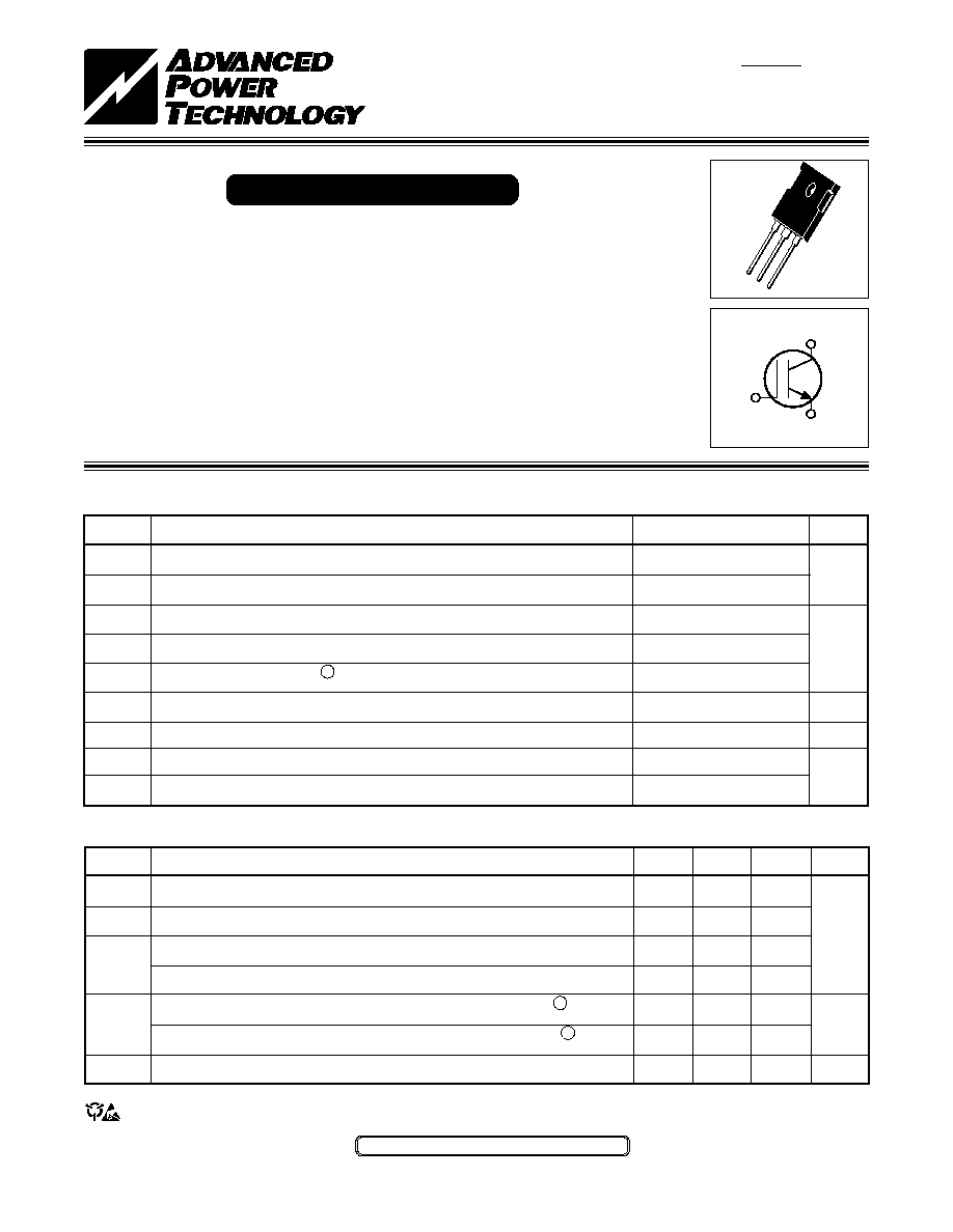
The Thunderblot
IGBT
Æ
is a new generation of high voltage power IGBTs. Using Non- Punch
Through Technology, the Thunderblot
IGBT
Æ
offers superior ruggedness and ultrafast
switching speed.
∑ Low Forward Voltage Drop
∑ High Freq. Switching to 50KHz
∑ Low Tail Current
∑ Ultra Low Leakage Current
∑ RBSOA and SCSOA Rated
Thunderbolt IGBT
Æ
1200V
APT15GT120BR
APT15GT120BRG*
*G Denotes RoHS Compliant, Pb Free Terminal Finish.
Æ
TO-2
47
G
C
E

050-6266 Rev B 12-2005
APT15GT120BR(G)
1
Repetitive Rating: Pulse width limited by maximum junction temperature.
2
For Combi devices, I
ces
includes both IGBT and FRED leakages
3
See MIL-STD-750 Method 3471.
4
E
on1
is the clamped inductive turn-on energy of the IGBT only, without the effect of a commutating diode reverse recovery current
adding to the IGBT turn-on loss. Tested in inductive switching test circuit shown in figure 21, but with a Silicon Carbide diode.
5
E
on2
is the clamped inductive turn-on energy that includes a commutating diode reverse recovery current in the IGBT turn-on switching
loss. (See Figures 21, 22.)
6
E
off
is the clamped inductive turn-off energy measured in accordance with JEDEC standard JESD24-1. (See Figures 21, 23.)
APT Reserves the right to change, without notice, the specifications and information contained herein.
THERMAL AND MECHANICAL CHARACTERISTICS
UNIT
∞C/W
gm
MIN
TYP
MAX
.50
N/A
5.9
Characteristic
Junction to Case
(IGBT)
Junction to Case
(DIODE)
Package Weight
Symbol
R
JC
R
JC
W
T
DYNAMIC CHARACTERISTICS
Symbol
C
ies
C
oes
C
res
V
GEP
Q
g
Q
ge
Q
gc
SSOA
t
d(on)
t
r
t
d(off)
t
f
E
on1
E
on2
E
off
t
d(on)
t
r
t
d(off)
t
f
E
on1
E
on2
E
off
Test Conditions
Capacitance
V
GE
= 0V, V
CE
= 25V
f = 1 MHz
Gate Charge
V
GE
= 15V
V
CE
= 600V
I
C
= 15A
T
J
= 150∞C, R
G
= 5, V
GE
=
15V, L = 100µH,V
CE
= 960V
Inductive Switching (25∞C)
V
CC
= 800V
V
GE
= 15V
I
C
= 15A
R
G
= 5
T
J
= +25∞C
Inductive Switching (125∞C)
V
CC
= 800V
V
GE
= 15V
I
C
= 15A
R
G
= 5
T
J
= +125∞C
Characteristic
Input Capacitance
Output Capacitance
Reverse Transfer Capacitance
Gate-to-Emitter Plateau Voltage
Total Gate Charge
3
Gate-Emitter Charge
Gate-Collector ("Miller") Charge
Switching Safe Operating Area
Turn-on Delay Time
Current Rise Time
Turn-off Delay Time
Current Fall Time
Turn-on Switching Energy
4
Turn-on Switching Energy (Diode)
5
Turn-off Switching Energy
6
Turn-on Delay Time
Current Rise Time
Turn-off Delay Time
Current Fall Time
Turn-on Switching Energy
4
4
Turn-on Switching Energy (Diode)
5
5
Turn-off Switching Energy
6
MIN
TYP
MAX
1070
100
65
10
105
10
60
45
10
11
85
35
585
800
260
10
11
95
42
590
1440
340
UNIT
pF
V
nC
A
ns
µ
J
ns
µ
J

050-6266 Rev B 12-2005
APT15GT120BR(G)
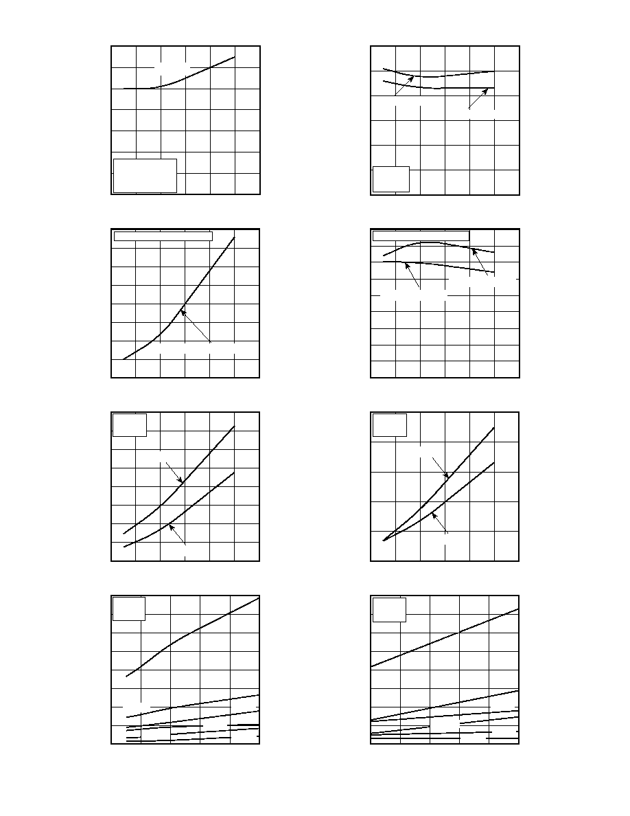
TYPICAL PERFORMANCE CURVES
V
GS(TH)
, THRESHOLD VOLTAGE
V
CE
, COLLECTOR-TO-EMITTER VOLTAGE (V)
I
C
, COLLECTOR CURRENT (A)
I
C
, COLLECTOR CURRENT (A)
(NORMALIZED)
I
C,
DC COLLECTOR CURRENT(A)
V
CE
, COLLECTOR-TO-EMITTER VOLTAGE (V)
V
GE
, GATE-TO-EMITTER VOLTAGE (V)
I
C
, COLLECTOR CURRENT (A)
250µs PULSE
TEST<0.5 % DUTY
CYCLE
60
50
40
30
20
10
0
16
14
12
10
8
6
4
2
0
6
5
4
3
2
1
0
45
40
35
30
25
20
15
10
5
0
14V
12V
11V
10V
13V
9V
8V
T
J
= 125∞C
T
J
= 25∞C
T
J
= -55∞C
V
GE
= 15V.
250µs PULSE TEST
<0.5 % DUTY CYCLE
T
J
= 125∞C
T
J
= 25∞C
T
J
= -55∞C
15V
45
40
35
30
25
20
15
10
5
0
45
40
35
30
25
20
15
10
5
0
6
5
4
3
2
1
0
1.10
1.05
1.00
0.95
0.90
0.85
0.80
0.75
V
CE
, COLLECTER-TO-EMITTER VOLTAGE (V)
V
CE
, COLLECTER-TO-EMITTER VOLTAGE (V)
FIGURE 1, Output Characteristics(T
J
= 25∞C)
FIGURE 2, Output Characteristics (T
J
= 125∞C)
V
GE
, GATE-TO-EMITTER VOLTAGE (V)
GATE CHARGE (nC)
FIGURE 3, Transfer Characteristics
FIGURE 4, Gate Charge
V
GE
, GATE-TO-EMITTER VOLTAGE (V)
T
J
, Junction Temperature (∞C)
FIGURE 5, On State Voltage vs Gate-to- Emitter Voltage
FIGURE 6, On State Voltage vs Junction Temperature
T
J
, JUNCTION TEMPERATURE (∞C)
T
C
, CASE TEMPERATURE (∞C)
FIGURE 7, Threshold Voltage vs. Junction Temperature
FIGURE 8, DC Collector Current vs Case Temperature
0
1
2
3
4
5
6
7
0
5
10
15
20
25
30
0
2
4
6
8
10
12
14
0
20
40
60
80
100
120
9
10
11
12
13
14
15
16
-50 -25
0
25
50
75
100 125
-50 -25
0
25 50 75 100 125 150
-50 -25
0
25 50 75 100 125 150
V
CE
=
960V
V
CE
= 600V
V
CE
= 240V
I
C
= 15A
T
J
= 25∞C
T
J
= 25∞C.
250µs PULSE TEST
<0.5 % DUTY CYCLE
I
C
= 30A
I
C
= 15A
I
C
= 7.5A
I
C
= 30A
I
C
= 15A
I
C
= 7.5A
V
GE
= 15V
050-6266 Rev B 12-2005
APT15GT120BR(G)
V
GE
=15V,T
J
=125∞C
V
GE
=15V,T
J
=25∞C
V
CE
=
800V
R
G
=
5
L = 100 µH
SWITCHING ENERGY LOSSES (µJ)
E
ON2
, TURN ON ENERGY LOSS (µJ)
t
r,
RISE TIME (ns)
t
d(ON)
, TURN-ON DELAY TIME (ns)
SWITCHING ENERGY LOSSES (µJ)
E
OFF
, TURN OFF ENERGY LOSS (µJ)
t
f,
FALL TIME (ns)
t
d
(OFF)
, TURN-OFF DELAY TIME (ns)
I
CE
, COLLECTOR TO EMITTER CURRENT (A)
I
CE
, COLLECTOR TO EMITTER CURRENT (A)
FIGURE 9, Turn-On Delay Time vs Collector Current
FIGURE 10, Turn-Off Delay Time vs Collector Current
I
CE
, COLLECTOR TO EMITTER CURRENT (A)
I
CE
, COLLECTOR TO EMITTER CURRENT (A)
FIGURE 11, Current Rise Time vs Collector Current
FIGURE 12, Current Fall Time vs Collector Current
I
CE
, COLLECTOR TO EMITTER CURRENT (A)
I
CE
, COLLECTOR TO EMITTER CURRENT (A)
FIGURE 13, Turn-On Energy Loss vs Collector Current
FIGURE 14, Turn Off Energy Loss vs Collector Current
R
G
, GATE RESISTANCE (OHMS)
T
J
, JUNCTION TEMPERATURE (∞C)
FIGURE 15, Switching Energy Losses vs. Gate Resistance
FIGURE 16, Switching Energy Losses vs Junction Temperature
V
CE
= 600V
T
J
= 25∞C
,
T
J
=125∞C
R
G
= 5
L = 100 µH
14
12
10
8
6
4
2
0
40
35
30
25
20
15
10
5
0
4000
3500
3000
2500
2000
1500
1000
500
0
8000
7000
6000
5000
4000
3000
2000
1000
0
120
100
80
60
40
20
0
45
40
35
30
25
20
15
10
5
0
1000
800
600
400
200
0
4000
3500
3000
2500
2000
1500
1000
500
0
V
GE
= 15V
V
CE
= 800V
V
GE
= +15V
R
G
= 5
5
10
15
20
25
30
35
5
10
15
20
25
30
35
5
10
15
20
25
30
35
5
10
15
20
25
30
35
5
10
15
20
25
30
35
5
10
15
20
25
30
35
0
10
20
30
40
50
0
25
50
75
100
125
R
G
=
5, L
=
100
µ
H, V
CE
=
800V
R
G
=
5, L
=
100
µ
H, V
CE
=
800V
T
J
=
25 or 125∞C,V
GE
=
15V
T
J
=
125∞C, V
GE
=
15V
T
J
=
25∞C, V
GE
=
15V
V
CE
= 800V
V
GE
= +15V
R
G
= 5
T
J
=
125∞C
T
J
=
25∞C
V
CE
= 800V
V
GE
= +15V
R
G
= 5
T
J
=
125∞C
T
J
=
25∞C
E
on2,
30A
E
off,
30A
V
CE
= 800V
V
GE
= +15V
T
J
= 125∞C
E
on2,
15A
E
off,
15A
E
on2,
7.5A
E
off,
7.5A
E
on2,
30A
E
off,
30A
E
on2,
15A
E
off,
15A
E
on2,
7.5A
E
off,
7.5A

050-6266 Rev B 12-2005
APT15GT120BR(G)
TYPICAL PERFORMANCE CURVES
0.60
0.50
0.40
0.30
0.20
0.10
0
Z
JC
, THERMAL IMPEDANCE (∞C/W)
0.3
0.7
SINGLE PULSE
RECTANGULAR PULSE DURATION (SECONDS)
Figure 19a, Maximum Effective Transient Thermal Impedance, Junction-To-Case vs Pulse Duration
10
-5
10
-4
10
-3
10
-2
10
-1
1.0
2,000
1,000
500
100
50
10
50
45
40
35
30
25
20
15
10
5
0
C, CAPACITANCE (
P
F)
I
C
, COLLECTOR CURRENT (A)
V
CE
, COLLECTOR-TO-EMITTER VOLTAGE (VOLTS)
V
CE
, COLLECTOR TO EMITTER VOLTAGE
Figure 17, Capacitance vs Collector-To-Emitter Voltage
Figure 18,Minimim Switching Safe Operating Area
0
10
20
30
40
50
0
200 400 600 800 1000 1200 1400
FIGURE 19b, TRANSIENT THERMAL IMPEDANCE MODEL
0
5
10
15
20
25
30
F
MAX
, OPERATING FREQUENCY (kHz)
I
C
, COLLECTOR CURRENT (A)
Figure 20, Operating Frequency vs Collector Current
T
J
= 125
∞
C
T
C
= 75
∞
C
D = 50 %
V
CE
= 800V
R
G
= 5
400
100
50
10
5
1
C
ies
0.5
0.1
0.05
F
max
=
min (f
max
, f
max2
)
0.05
f
max1
=
t
d(on)
+ t
r
+ t
d(off)
+ t
f
P
diss
- P
cond
E
on2
+ E
off
f
max2
=
P
diss
=
T
J
- T
C
R
JC
Peak TJ = PDM x ZJC + TC
Duty Factor D =
t1
/
t2
t2
t1
P
DM
Note:
C
oes
C
res
0.271
0.229
0.00471
0.0898
Power
(watts)
RC MODEL
Junction
temp. (∞C)
Case temperature. (∞C)
D = 0.9
050-6266 Rev B 12-2005
APT15GT120BR(G)
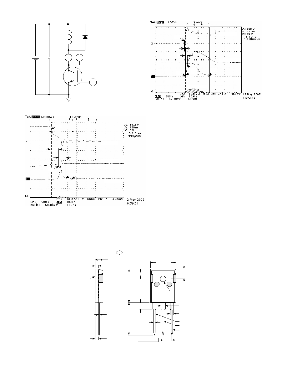
Figure 22, Turn-on Switching Waveforms and Definitions
Figure 23, Turn-off Switching Waveforms and Definitions
T
J
= 125∞C
Collector Current
Collector Voltage
Gate Voltage
Switching Energy
5%
10%
t
d(on)
90%
10%
t
r
5%
T
J
= 125∞C
Collector Voltage
Collector Current
Gate Voltage
Switching Energy
0
90%
t
d(off)
10%
t
f
90%
I
C
A
D.U.T.
V
CE
Figure 21, Inductive Switching Test Circuit
V
CC
APT15DQ120
APT's products are covered by one or more of U.S.patents 4,895,810 5,045,903 5,089,434 5,182,234 5,019,522
5,262,336 6,503,786 5,256,583 4,748,103 5,283,202 5,231,474 5,434,095 5,528,058 and foreign patents. US and Foreign patents pending. All Rights Reserved.
TO-247 Package Outline
e1 SAC: Tin, Silver, Copper
15.49 (.610)
16.26 (.640)
5.38 (.212)
6.20 (.244)
6.15 (.242) BSC
4.50 (.177) Max.
19.81 (.780)
20.32 (.800)
20.80 (.819)
21.46 (.845)
1.65 (.065)
2.13 (.084)
1.01 (.040)
1.40 (.055)
3.50 (.138)
3.81 (.150)
2.87 (.113)
3.12 (.123)
4.69 (.185)
5.31 (.209)
1.49 (.059)
2.49 (.098)
2.21 (.087)
2.59 (.102)
0.40 (.016)
0.79 (.031)
C
ollector
Collector
Emitter
Gate
5.45 (.215) BSC
Dimensions in Millimeters and (Inches)
2-Plcs.