APTGF125X60E3
A
P
T
G
F
1
2
5
X
6
0
E
3
≠
R
e
v
0
J
u
l
y
,
2
0
0
3
APT website ≠ http://www.advancedpower.com
1 - 3
Absolute maximum ratings
Symbol
Parameter
Max ratings
Unit
V
CES
Collector - Emitter Breakdown Voltage
600
V
T
C
= 25∞C
180
I
C
Continuous Collector Current
T
C
= 80∞C
125
I
CM
Pulsed Collector Current
T
C
= 25∞C
350
A
V
GE
Gate ≠ Emitter Voltage
±20
V
P
D
Maximum Power Dissipation
T
C
= 25∞C
570
W
RBSOA Reverse Bias Safe Operating Area
T
j
= 125∞C
300A@480V
These Devices are sensitive to Electrostatic Discharge. Proper Handing Procedures Should Be Followed.
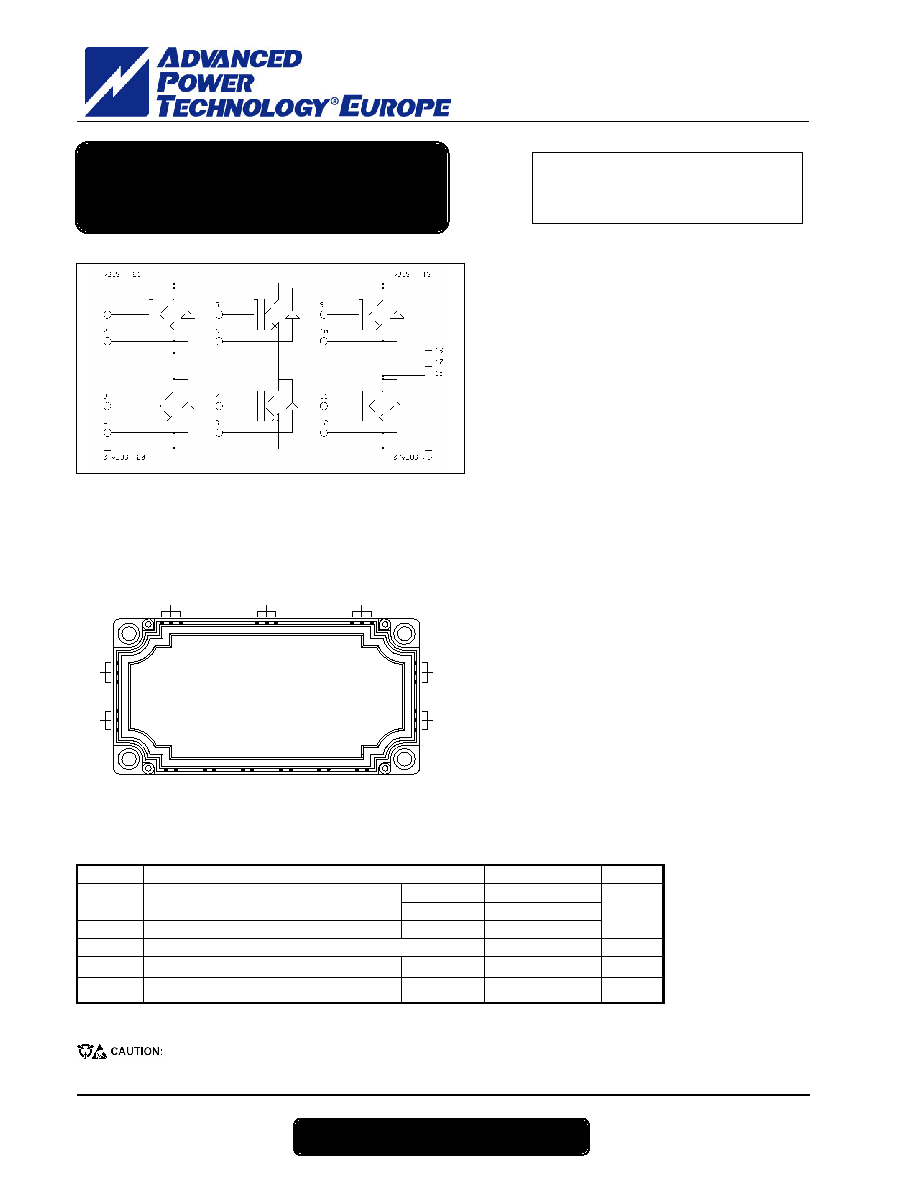
13
14
17
19
15
8
9
11
10
12
21
20
5 6
3 4
1 2
7
V
CES
= 600V
I
C
= 125A @ Tc = 80∞C
Application
∑ AC Motor control
Features
∑ Non Punch Through (NPT) Fast IGBT
Æ
-
Low voltage drop
-
Low tail current
-
Switching frequency up to 50 kHz
-
Soft recovery parallel diodes
-
Low diode VF
-
Low leakage current
-
Avalanche energy rated
-
RBSOA and SCSOA rated
∑ Kelvin emitter for easy drive
∑ Very low stray inductance
∑ High level of integration
Benefits
∑ Outstanding performance at high frequency
operation
∑ Stable temperature behavior
∑ Very rugged
∑ Solderable terminals for easy PCB mounting
∑ Direct mounting to heatsink (isolated package)
∑ Low junction to case thermal resistance
∑ Easy paralleling due to positive TC of VCEsat
∑ Low profile
3 Phase bridge
NPT IGBT Power Module
APTGF125X60E3
A
P
T
G
F
1
2
5
X
6
0
E
3
≠
R
e
v
0
J
u
l
y
,
2
0
0
3
APT website ≠ http://www.advancedpower.com
2 - 3
Electrical Characteristics
All ratings @ T
j
= 25∞C unless otherwise specified
Symbol Characteristic
Test Conditions
Min Typ Max Unit
BV
CES
Collector - Emitter Breakdown Voltage
V
GE
= 0V, I
C
= 500µA
600
V
T
j
= 25∞C
1
500
µA
I
CES
Zero Gate Voltage Collector Current
V
GE
= 0V
V
CE
= 600V
T
j
= 125∞C
1
mA
T
j
= 25∞C
1.7
2.0
2.45
V
CE(on)
Collector Emitter on Voltage
V
GE
=15V
I
C
= 150A
T
j
= 125∞C
2.2
V
V
GE(th)
Gate Threshold Voltage
V
GE
= V
CE
, I
C
= 3 mA
4.5
6.5
V
I
GES
Gate ≠ Emitter Leakage Current
V
GE
= 20V, V
CE
= 0V
450
nA
Dynamic Characteristics
Symbol Characteristic
Test Conditions
Min Typ Max Unit
C
ies
Input Capacitance
6500
C
res
Reverse Transfer Capacitance
V
GE
= 0V, V
CE
= 25V
f = 1MHz
600
pF
T
d(on)
Turn-on Delay Time
115
T
r
Rise Time
28
T
d(off)
Turn-off Delay Time
200
T
f
Fall Time
Inductive Switching (25∞C)
V
GE
= ±15V
V
Bus
= 300V
I
C
= 150A
R
G
= 1.5
25
ns
T
d(on)
Turn-on Delay Time
125
T
r
Rise Time
30
T
d(off)
Turn-off Delay Time
225
T
f
Fall Time
35
ns
E
off
Turn off Energy
Inductive Switching (125∞C)
V
GE
= ±15V
V
Bus
= 300V
I
C
= 150A
R
G
= 1.5
4.6
mJ
Reverse diode ratings and characteristics
Symbol Characteristic
Test Conditions
Min Typ Max Unit
T
j
= 25∞C
1.25
1.6
V
F
Diode Forward Voltage
I
F
= 150A
V
GE
= 0V
T
j
= 125∞C
1.2
V
E
r
Reverse Recovery Energy
I
F
= 150A
V
R
= 300V
di/dt =800A/µs
T
j
= 125∞C
4.7
mJ
T
j
= 25∞C
10
Q
rr
Reverse Recovery Charge
I
F
= 150A
V
R
= 300V
di/dt =800A/µs T
j
= 125∞C
18
µC
Thermal and package characteristics
Symbol Characteristic
Min Typ Max Unit
IGBT
0.22
R
thJC
Junction to Case
Diode
0.44
∞C/W
V
ISOL
RMS Isolation Voltage, any terminal to case t =1 min,
I isol<1mA, 50/60Hz
2500
V
T
J
Operating junction temperature range
-40
150
T
STG
Storage Temperature Range
-40
125
T
C
Operating Case Temperature
-40
125
∞C
Torque Mounting torque
To heatsink
M5
3
4.5
N.m
Wt
Package Weight
300
g
APTGF125X60E3
A
P
T
G
F
1
2
5
X
6
0
E
3
≠
R
e
v
0
J
u
l
y
,
2
0
0
3
APT website ≠ http://www.advancedpower.com
3 - 3
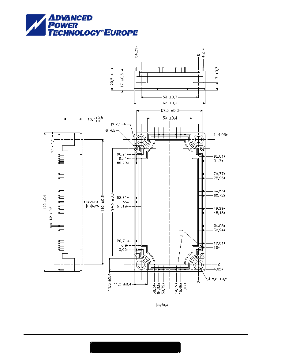
Package outline
PIN 1
PIN 21
ALL DIMENSIONS MARKED " * " ARE TOLERENCED AS :
APT reserves the right to change, without notice, the specifications and information contained herein
APT's products are covered by one or more of U.S patents 4,895,810 5,045,903 5,089,434 5,182,234 5,019,522
5,262,336 6,503,786 5,256,583 4,748,103 5,283,202 5,231,474 5,434,095 5,528,058 and foreign patents. U.S and Foreign patents pending. All Rights Reserved.