APTGT150A120D3
A
P
T
G
T
1
5
0
A
1
2
0
D
3
≠
R
e
v
0
J
a
n
u
a
r
y
,
2
0
0
4
APT website ≠ http://www.advancedpower.com
1 - 3
Absolute maximum ratings
Symbol
Parameter
Max ratings
Unit
V
CES
Collector - Emitter Breakdown Voltage
1200
V
T
C
= 25∞C
220
I
C
Continuous Collector Current
T
C
= 80∞C
150
I
CM
Pulsed Collector Current
T
C
= 25∞C
350
A
V
GE
Gate ≠ Emitter Voltage
±20
V
P
D
Maximum Power Dissipation
T
C
= 25∞C
695
W
SCSOA Short Circuit Safe Operating Area
T
j
= 125∞C
600A@900V
These Devices are sensitive to Electrostatic Discharge. Proper Handing Procedures Should Be Followed.
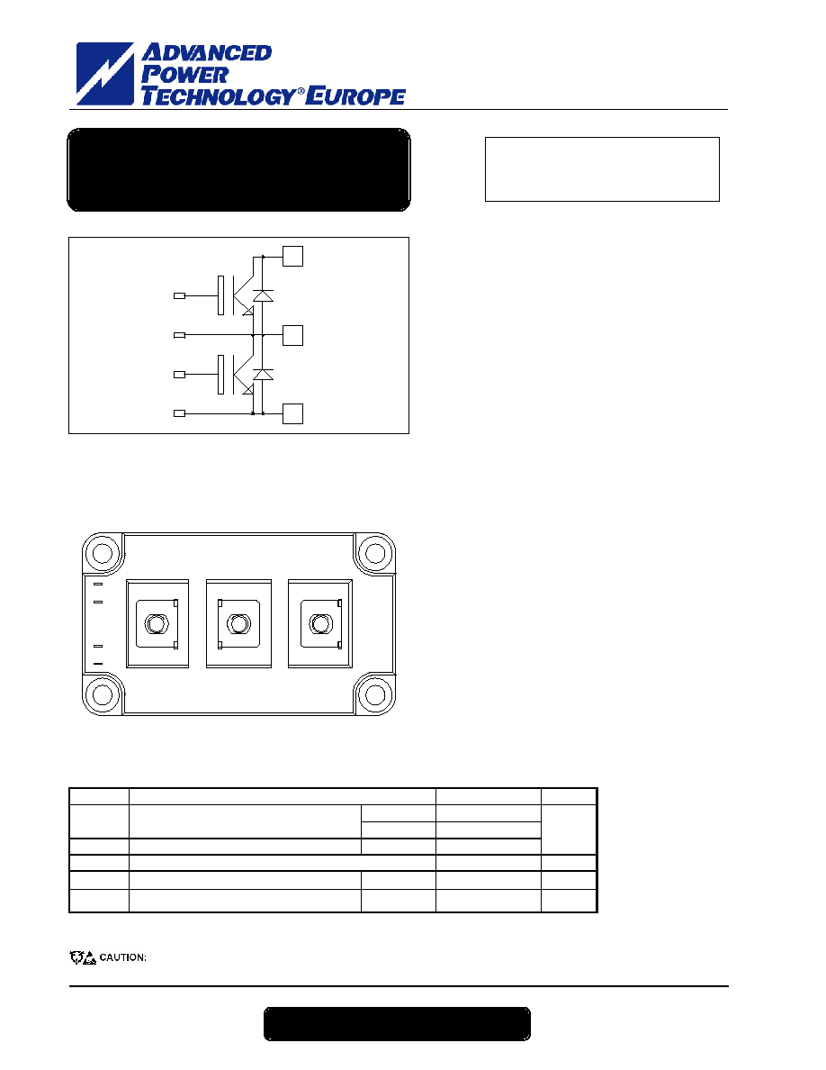
2
1
3
5
Q2
7
6
Q1
4
2
3
5
4
6
7
1
V
CES
= 1200V
I
C
= 150A @ Tc = 80∞C
Application
∑ Welding converters
∑ Switched Mode Power Supplies
∑ Uninterruptible Power Supplies
∑ Motor control
Features
∑ Trench + Field Stop IGBT
Æ
Technology
-
Low voltage drop
-
Low tail current
-
Switching frequency up to 20 kHz
-
Soft recovery parallel diodes
-
Low diode VF
-
Low leakage current
-
Avalanche energy rated
-
RBSOA and SCSOA rated
∑ Kelvin emitter for easy drive
∑ Low stray inductance
-
M6 power connectors
∑ High level of integration
Benefits
∑ Outstanding performance at high frequency
operation
∑ Stable temperature behavior
∑ Very rugged
∑ Direct mounting to heatsink (isolated package)
∑ Low junction to case thermal resistance
∑ Easy paralleling due to positive TC of VCEsat
Phase Leg
Trench IGBT
Æ
Power Module
APTGT150A120D3
A
P
T
G
T
1
5
0
A
1
2
0
D
3
≠
R
e
v
0
J
a
n
u
a
r
y
,
2
0
0
4
APT website ≠ http://www.advancedpower.com
2 - 3
All ratings @ T
j
= 25∞C unless otherwise specified
Electrical Characteristics
Symbol Characteristic
Test Conditions
Min Typ Max Unit
BV
CES
Collector - Emitter Breakdown Voltage
V
GE
= 0V, I
C
= 6mA
1200
V
I
CES
Zero Gate Voltage Collector Current
V
GE
= 0V, V
CE
= 1200V
4
mA
T
j
= 25∞C
1.7
2.1
V
CE(on)
Collector Emitter on Voltage
V
GE
= 15V
I
C
= 150A
T
j
= 125∞C
2.0
V
V
GE(th)
Gate Threshold Voltage
V
GE
= V
CE
, I
C
= 6mA
5.0
5.8
6.5
V
I
GES
Gate ≠ Emitter Leakage Current
V
GE
= 20V, V
CE
= 0V
600
nA
Dynamic Characteristics
Symbol Characteristic
Test Conditions
Min Typ Max Unit
C
ies
Input Capacitance
10.7
C
oes
Output Capacitance
0.56
C
res
Reverse Transfer Capacitance
V
GE
= 0V
V
CE
= 25V
f = 1MHz
0.5
nF
T
d(on)
Turn-on Delay Time
280
T
r
Rise Time
90
T
d(off)
Turn-off Delay Time
550
T
f
Fall Time
Inductive Switching (25∞C)
V
GE
= ±15V
V
Bus
= 600V
I
C
= 150A
R
G
= 2.2
130
ns
T
d(on)
Turn-on Delay Time
290
T
r
Rise Time
100
T
d(off)
Turn-off Delay Time
650
T
f
Fall Time
Inductive Switching (125∞C)
V
GE
= ±15V
V
Bus
= 600V
I
C
= 150A
R
G
= 2.2
180
ns
Reverse diode ratings and characteristics
Symbol Characteristic
Test Conditions
Min Typ Max Unit
T
j
= 25∞C
1.6
2.1
V
F
Diode Forward Voltage
I
F
= 150A
V
GE
= 0V
T
j
= 125∞C
1.6
V
E
rec
Reverse Recovery Energy
I
F
= 150A
V
R
= 600V
di/dt =900A/µs
T
j
= 125∞C
12
mJ
T
j
= 25∞C
14
Q
rr
Reverse Recovery Charge
I
F
= 150A
V
R
= 600V
di/dt =900A/µs T
j
= 125∞C
28
µC
Thermal and package characteristics
Symbol Characteristic
Min Typ Max Unit
IGBT
0.18
R
thJC
Junction to Case
Diode
0.30
∞C/W
V
ISOL
RMS Isolation Voltage, any terminal to case t =1 min,
I isol<1mA, 50/60Hz
2500
V
T
J
Operating junction temperature range
-40
150
T
STG
Storage Temperature Range
-40
125
T
C
Operating Case Temperature
-40
125
∞C
For terminals
M6
3
5
Torque Mounting torque
To Heatsink
M6
3
5
N.m
Wt
Package Weight
380
g
APTGT150A120D3
A
P
T
G
T
1
5
0
A
1
2
0
D
3
≠
R
e
v
0
J
a
n
u
a
r
y
,
2
0
0
4
APT website ≠ http://www.advancedpower.com
3 - 3
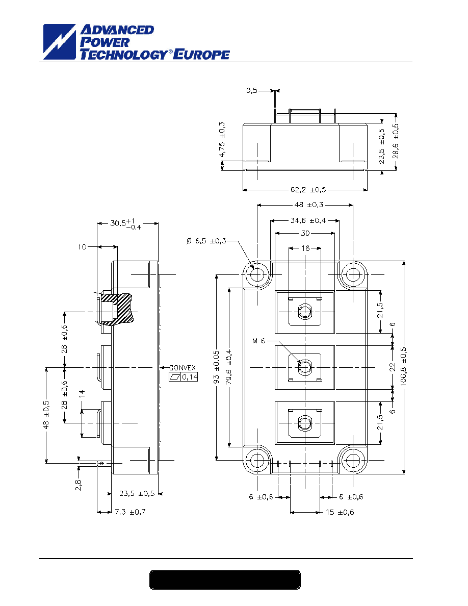
Package outline
APT reserves the right to change, without notice, the specifications and information contained herein
APT's products are covered by one or more of U.S patents 4,895,810 5,045,903 5,089,434 5,182,234 5,019,522
5,262,336 6,503,786 5,256,583 4,748,103 5,283,202 5,231,474 5,434,095 5,528,058 and foreign patents. U.S and Foreign patents pending. All Rights Reserved.