APTGT50A120T
A
P
T
G
T
5
0
A
120T
≠ R
e
v 0 M
a
y, 2005
APT website ≠ http://www.advancedpower.com
1 - 5
Absolute maximum ratings
Symbol Parameter
Max
ratings
Unit
V
CES
Collector - Emitter Breakdown Voltage
1200
V
T
C
= 25∞C
75
I
C
Continuous
Collector
Current
T
C
= 80∞C
50
I
CM
Pulsed Collector Current
T
C
= 25∞C
100
A
V
GE
Gate ≠ Emitter Voltage
±20
V
P
D
Maximum Power Dissipation
T
C
= 25∞C
277 W
RBSOA Reverse Bias Safe Operating Area
T
j
= 125∞C
100A @ 1150V
These Devices are sensitive to Electrostatic Discharge. Proper Handing Procedures Should Be Followed.
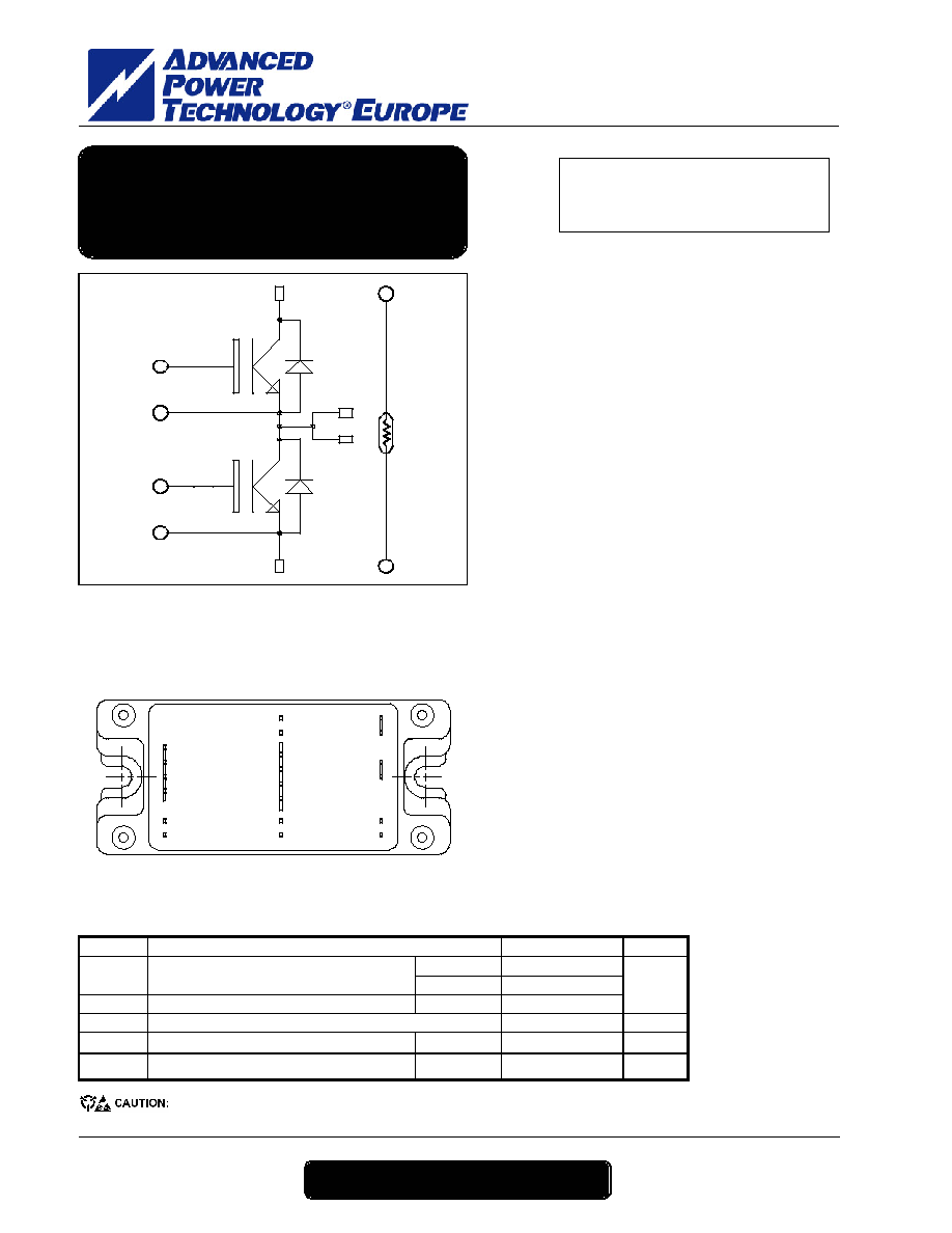
VBUS
Q1
G1
E1
OUT
NTC2
0/VBU S
G2
E2
NTC1
Q2
OUT
OUT
NTC2
VBUS
E1
G2
E2
NTC1
0/VBUS
G2
E2
G1
V
CES
= 1200V
I
C
= 50A @ Tc = 80∞C
Application
∑ Welding converters
∑ Switched Mode Power Supplies
∑ Uninterruptible Power Supplies
∑ Motor control
Features
∑ Fast Trench + Field Stop IGBT
Æ
Technology
- Low voltage drop
- Low tail current
- Switching frequency up to 20 kHz
- Soft recovery parallel diodes
- Low diode VF
- Low leakage current
- Avalanche energy rated
- RBSOA and SCSOA rated
∑ Kelvin emitter for easy drive
∑ Very low stray inductance
- Symmetrical design
- Lead frames for power connections
∑ High level of integration
∑ Internal thermistor for temperature monitoring
Benefits
∑ Stable temperature behavior
∑ Very rugged
∑ Solderable terminals for easy PCB mounting
∑ Direct mounting to heatsink (isolated package)
∑ Low junction to case thermal resistance
∑ Easy paralleling due to positive TC of VCEsat
∑ Low profile
Phase leg
Fast Trench + Field Stop IGBT
Æ
Power Module
APTGT50A120T
A
P
T
G
T
5
0
A
120T
≠ R
e
v 0 M
a
y, 2005
APT website ≠ http://www.advancedpower.com
2 - 5
All ratings @ T
j
= 25∞C unless otherwise specified
Electrical Characteristics
Symbol Characteristic
Test
Conditions
Min Typ Max Unit
I
CES
Zero Gate Voltage Collector Current
V
GE
= 0V, V
CE
= 1200V
500
µA
T
j
= 25∞C
1.7 2.1
V
CE(sat)
Collector Emitter Saturation Voltage
V
GE
= 15V
I
C
= 50A
T
j
= 125∞C
2.0
V
V
GE(th)
Gate
Threshold
Voltage
V
GE
= V
CE
, I
C
= 2mA
5.0
5.8
6.5
V
I
GES
Gate ≠ Emitter Leakage Current
V
GE
= 20V, V
CE
= 0V
400
nA
Dynamic Characteristics
Symbol Characteristic
Test
Conditions
Min Typ Max Unit
C
ies
Input
Capacitance
3600
C
oes
Output
Capacitance
190
C
res
Reverse Transfer Capacitance
V
GE
= 0V
V
CE
= 25V
f = 1MHz
160
pF
T
d(on)
Turn-on Delay Time
90
T
r
Rise Time
30
T
d(off)
Turn-off Delay Time
420
T
f
Fall Time
Inductive Switching (25∞C)
V
GE
= 15V
V
Bus
= 600V
I
C
= 50A
R
G
= 18
70
ns
T
d(on)
Turn-on
Delay
Time
90
T
r
Rise Time
50
T
d(off)
Turn-off Delay Time
520
T
f
Fall Time
90
ns
E
on
Turn-on Switching Energy
5
E
off
Turn-off Switching Energy
Inductive Switching (125∞C)
V
GE
= 15V
V
Bus
= 600V
I
C
= 50A
R
G
= 18
5.5
mJ
Reverse diode ratings and characteristics
Symbol Characteristic
Test
Conditions
Min Typ Max Unit
V
RRM
Maximum Peak Repetitive Reverse Voltage
1200
V
T
j
= 25∞C
250
I
RM
Maximum Reverse Leakage Current
V
R
=1200V
T
j
= 125∞C
500
µA
I
F(A V)
Maximum Average Forward Current
50% duty cycle
Tc = 80∞C
50
A
T
j
= 25∞C
1.4
1.9
V
F
Diode Forward Voltage
I
F
= 50A
T
j
= 125∞C
1.3
V
T
j
= 25∞C
150
t
rr
Reverse Recovery Time
T
j
= 125∞C
250
ns
T
j
= 25∞C
4.5
Q
rr
Reverse Recovery Charge
I
F
= 50A
V
R
= 600V
di/dt =2000A/µs
T
j
= 125∞C
9
µC

APTGT50A120T
A
P
T
G
T
5
0
A
120T
≠ R
e
v 0 M
a
y, 2005
APT website ≠ http://www.advancedpower.com
3 - 5
Temperature sensor NTC
(see application note APT0406 on www.advancedpower.com for more information).
Symbol Characteristic
Min Typ Max Unit
R
25
Resistance @ 25∞C
50
k
B
25/85
T
25
= 298.15 K
3952
K
-
=
T
T
B
R
R
T
1
1
exp
25
85
/
25
25
Thermal and package characteristics
Symbol Characteristic
Min Typ Max Unit
IGBT
0.45
R
thJC
Junction
to
Case
Diode
0.58
∞C/W
V
ISOL
RMS Isolation Voltage, any terminal to case t =1 min, I isol<1mA, 50/60Hz
2500 V
T
J
Operating junction temperature range
-40
150
T
STG
Storage Temperature Range
-40
125
T
C
Operating Case Temperature
-40
100
∞C
Torque Mounting torque
To Heatsink
M5
1.5
4.7
N.m
Wt Package
Weight
160 g
Package outline
(dimensions in mm)
T: Thermistor temperature
R
T
: Thermistor value at T

APTGT50A120T
A
P
T
G
T
5
0
A
120T
≠ R
e
v 0 M
a
y, 2005
APT website ≠ http://www.advancedpower.com
4 - 5
Typical Performance Curve
Output Characteristics (V
GE
=15V)
T
J
=25∞C
T
J
=125∞C
0
20
40
60
80
100
0
0.5
1
1.5
2
2.5
3
3.5
V
CE
(V)
I
C
(A
)
Output Characteristics
V
GE
=15V
V
GE
=13V
V
GE
=17V
V
GE
=9V
0
20
40
60
80
100
0
1
2
3
4
V
CE
(V)
I
C
(A
)
T
J
= 125∞C
Transfert Characteristics
T
J
=25∞C
T
J
=125∞C
T
J
=125∞C
0
20
40
60
80
100
5
6
7
8
9
10
11
12
V
GE
(V)
I
C
(A
)
Energy losses vs Collector Current
Eon
Eon
Eoff
Er
0
2
4
6
8
10
12
0
20
40
60
80
100
I
C
(A)
E (
m
J
)
V
CE
= 600V
V
GE
= 15V
R
G
= 18
T
J
= 125∞C
Eon
Eoff
Er
0
2
4
6
8
10
12
0
10
20
30
40
50
60
70
80
Gate Resistance (ohms)
E (
m
J
)
V
CE
= 600V
V
GE
=15V
I
C
= 50A
T
J
= 125∞C
Switching Energy Losses vs Gate Resistance
Reverse Bias Safe Operating Area
0
20
40
60
80
100
120
0
300
600
900
1200
1500
V
CE
(V)
I
C
(A
)
V
GE
=15V
T
J
=125∞C
R
G
=18
maximum Effective Transient Thermal Impedance, Junction to Pulse Duration
0.9
0.7
0.5
0.3
0.1
0.05
Single Pulse
0
0.1
0.2
0.3
0.4
0.5
0.00001
0.0001
0.001
0.01
0.1
1
10
rectangular Pulse Duration (Seconds)
T
h
e
r
m
a
l Im
p
e
d
a
n
c
e
(
∞
C
/
W
)
IGBT

APTGT50A120T
A
P
T
G
T
5
0
A
120T
≠ R
e
v 0 M
a
y, 2005
APT website ≠ http://www.advancedpower.com
5 - 5
Forward Characteristic of diode
T
J
=25∞C
T
J
=125∞C
T
J
=125∞C
0
25
50
75
100
125
150
0
0.5
1
1.5
2
2.5
V
F
(V)
I
C
(A
)
hard
switching
ZCS
ZVS
0
10
20
30
40
50
60
70
80
0
10
20
30
40
50
60
70
80
I
C
(A)
Fm
a
x
,
O
p
e
r
a
t
i
ng Fr
e
que
nc
y
(
k
H
z
)
V
CE
=600V
D=50%
R
G
=18
T
J
=125∞C
T
C
=75∞C
Operating Frequency vs Collector Current
maximum Effective Transient Thermal Impedance, Junction to Pulse Duration
0.9
0.7
0.5
0.3
0.1
0.05
Single Pulse
0
0.1
0.2
0.3
0.4
0.5
0.6
0.00001
0.0001
0.001
0.01
0.1
1
10
rectangular Pulse Duration (Seconds)
The
r
m
a
l
I
m
pe
da
nc
e
(
∞
C
/
W
)
Diode
APT reserves the right to change, without notice, the specifications and information contained herein
APT's products are covered by one or more of U.S patents 4,895,810 5,045,903 5,089,434 5,182,234 5,019,522
5,262,336 6,503,786 5,256,583 4,748,103 5,283,202 5,231,474 5,434,095 5,528,058 and foreign patents. U.S and Foreign patents pending. All Rights Reserved.