 | –≠–ª–µ–∫—Ç—Ä–æ–Ω–Ω—ã–π –∫–æ–º–ø–æ–Ω–µ–Ω—Ç: 1775 | –°–∫–∞—á–∞—Ç—å:  PDF PDF  ZIP ZIP |

SCDCT1775 Rev B
DESCRIPTION
The CT1775 Universal MACAIR/1553 Dumb Remote Terminal Unit (RTU) consists of a transceiver, and encoder/decoder, control
logic, dual rank I/O registers and internal clock oscillator packaged in a 1.6" x 1.9" hermetic hybrid. It provides all the functions
required to interface between a MACAIR (sinusodial) or MIL-STD-1553 (Trapezoidal) serial MUX data bus and a subsystem parallel
3-state data highway. Utilizing several ASIC ICs, the CT1775 provides sufficient handshaking, control and data lines to permit
versatile operation as a remote terminal, a bus controller or a bus monitor, in either single or dual redundant data bus configurations.
As a transmitter, the CT1775 accepts 8 bit or 16 bit parallel date from the subsystem, and outputs serial Manchester II coded
Command, Status or Data words, under subsystem control. As a receiver, it accepts serial MIL-STD-1553 or MACAIR transmissions
and transfers all Command, Status and Data words to the 8 bit or 16 bit data highway, under subsystem control. The CT1775 also
provides flags to the subsystem when Broadcast, Mode Code, and Own Address (with parity) commands are decoded.
The CT1775 contains a terminal fail-safe timeout circuit which flags message lengths exceeding 768µs, and terminates serial data
transmission. Wraparound selftest is initiated by a control line which causes the encoder serial output to be connected to the decoder
input. The CT1775 provides a serial output of decoded words, thus allowing Command Word look ahead, for the fastest terminal
response.
FEATURES
CT1775 Replaces DDC BUS-65201
Includes:
- Universal Transceiver
- Encoder/decoder
- Dual Rank I/O Registers
- Fail-safe Timer
- Clock Oscillator
Simple Controls for Single or Dual Redundant Data Bus Configurations
Provides Flags for:
- Own Address (With Parity)
- Mode Code
- Broadcast
- Time Out
- Valid Word
- Sync Type
16 Bit or 8 Bit 3-State
- Parallel I/O and Serial Out
Wraparound Built-In Test
MIL-PRF-38534 Compliant Circuits Available
Packaging ≠ Hermetic Metal
- 68 Pin, 1.85" x 1.6" x .19" Plug-In Type Package
CT1775
PRELIMINARY DATA SHEET
Universal MacAir/1553 Dumb RTU Hybrid
www.aeroflex.com/Avionics

2
SCDCT1775 Rev B
T/
O
DRI
V
E
R
FI
L
T
E
R
S
HAP
I
N
G
NE
T
W
O
R
K
S
HAP
I
N
G
NE
T
W
O
R
K
DRI
V
E
R
TX
T
X
DAT
A
T
X
DAT
A
FA
I
L
-
SA
F
E
DRI
V
E
R
I
NHI
BI
T
SY
N
C
SE
L
E
C
T
EN
C
E
NABL
E
CL
O
C
K
GE
N
CL
O
C
K
IN
CL
O
C
K
PO
W
E
R
XT
A
L
CL
O
C
K
OU
T
RX
ST
R
O
B
E
DE
C
RS
T
MR
ST
S/T
SE
L
E
C
T
ADDR
IN
DS
C
OU
T
EN
A
ADDR
PA
R
ADDR
PA
R
IN
5
T
AKE
DA
T
A
DA
T
A
SE
L
E
C
T
1
DA
T
A
SE
L
E
C
T
2
ES
C
OU
T
SE
N
D
DA
T
A
LA
T
C
H
DA
T
A
1
LO
A
D
DA
T
A
1
LOA
D
DA
T
A
2
LA
T
C
H
DA
T
A
2
S
E
RI
AL
D
A
T
A
I
N
D15 (
M
S
B
)
CHAN S
E
L
E
C
T
T
HRU
D0 (L
S
B
)
BDS
T
I
NHI
BI
T
BRO
ADCAS
T
M
O
DE
CO
DE
V
A
L
I
D W
O
RD
V
A
L
CM
D W
D
FA
I
L
-
S
A
F
E
CO
M
M
D
A
T
A
SY
N
C
RT
E
NABL
E
DAT
A
P
ARI
T
Y
BI
T
S
T
A
T
U
S
S
E
RI
AL
D
A
T
A
O
U
T
S
E
RI
AL
D
A
T
A
O
U
T
R
E
GI
S
T
ER
R
E
G
I
ST
ER
R
E
G
I
ST
ER
R
E
GI
S
T
ER
RX
D
A
T
A
RX
D
A
T
A
LI
M
I
TE
R
}
}
M
ANC
HE
S
T
E
R
DE
CO
D
E
R
AND
CO
NT
R
O
L
L
O
G
I
C
M
ANC
HE
S
T
E
R
E
NCO
D
E
R
AND
CO
NT
R
O
L
L
O
G
I
C
F
IGURE 1
≠
CT
1
7
7
5
BL
O
C
K DI
A
G
RAM
3
SCDCT1775 Rev B
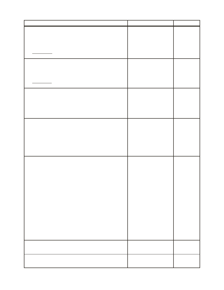
VALUES AT NOMINAL POWER SUPPLY VOLTAGES UNLESS OTHERWISE SPECIFIED
PARAMETER
VALUE
UNITS
Receiver
Differential Input Impedance
(DC to 1MHz)
4 min
K
Differential Input Voltage
40 max
V
P-P
Input Threshold (Direct Coupled)
1 typ
V
P-P
CMRR (DC to 2MHZ)
40 min
dB
CMV (DC to 2MHZ)
±10 min
V
RX STROBE Characteristics
1 typ
TTL Loads
Transmitter
Differential Output Voltage
Direct Coupled (across 145
Load)
30 typ
V
P-P
Transformer Coupled (at stub)
21 typ
V
P-P
Output Rise and Fall time
130 typ
ns
Output Noise
10 max
mV
P-P
TX INHIBIT Characteristics
1 typ
TTL Loads
Logic
I
IH
,
I
IL
,
I
OH
,
I
OL
See pin function &
loading Table
V
OH
2.5 min
V
V
OL
0.4 max
V
V
IH
2.0 min
V
V
IL
0.7 max
V
Clock
V
OHC
(Internal Clock)
Supply
-0.3 min
V
V
OLC
(Internal Clock)
Ground
+0.3 min
V
V
IHC
(External Clock)
Supply
-0.5 min
V
V
ILC
(External Clock)
Ground
+0.5 min
V
Power Supplies
+5V OSC/CLOCK Supply
Voltage Tolerances
±10
%
Current Drain
8 typ; 13 max
mA
+5V Logic Supply
Voltage Tolerances
±10
%
Current Drain
250 max
mA
+15V (or +12V) Supply
Voltage Tolerances
±5
%
Current Drain
65 max
mA
-15V Supply
Voltage Tolerances
±5
%
Current Drain
Idle
65 max
mA
25% Transmit
105 max
mA
100% Transmit
250 max
mA
-12V Supply
Voltage Tolerances
±5
%
Current Drain
Idle
65 max
mA
25% Transmit
105 max
mA
100% Transmit
250 max
mA
Temperature Range
Operating (Case)
-55 to +125
∞C
Storage
-65 to +150
∞C
Physical Characteristics
Size
68 pin DDIP
1.6 x 1.9 x 0.18
in
TABLE 1 ≠ CT1775 SPECIFICATIONS

4
SCDCT1775 Rev B
GENERAL
As shown in the block diagram of Figure 1, the CT1775
provides all functions required to implement a Dumb Remote
Terminal Unit (RTU). It is designed for the greatest flexibility
and ease of use. CT1775 can be operated with either an
internal or external clock. Simple control lines are provided to
interface with either single channel or dual redundant
configurations.
Control lines are available to implement either on line or off
line wraparound built-in test. CT1775 can be configured to
perform a parity check on its hard-wired terminal address. It
provides numerous output flags to simplify the use interface.
These flags indicate various decoded messages, as well as the
results of error checks. Sync selection, along with the flexible
controls, allows the CT1775 to operate as a Bus Controller as
well as a Remote Terminal.
INTERNAL OR EXTERNAL CLOCK
CT1775 may be operated with either its internal clock or an
external clock. Internal clock operation requires that a 12 MHz
parallel-resonant fundamental-mode crystal, such as
MIL-C-3098/42 TYPE CR64/U, be connected between pin 18
(XTAL) and ground. In addition, +5 volt power must be
connected to pin 2 (OSC/CLOCK POWER), and CLOCK
OUT (pin 19) must be connected to CLOCK in (pin 24).
For external clock operation, no connection is made to pin 2
(OSC/CLOCK POWER, and the external clock is applied to
pin 24 (CLOCK IN). Pin 19 (CLOCK OUT) is not connected.
The external clock must be capable of driving a load of 20
picofarads to within 0.5 volts of the + 5 volt power supply and
to within 0.5 volts of ground. Standard TTL voltage levels will
not work properly. It must have a rise time and fall time of less
than 10 nanoseconds. For compliance with MILSTD-1553, the
external clock frequency must be 12 MHz.
8 BIT OR 16 BIT INTERFACE
The CT1775 may be configured to interface with either 8 bit or
16 bit parallel data highways. For 16 bit operation, the 16 data
lines (D 15 through DO) are used directly. LATCH DATA 1
and LATCH DATA 2 are tied together, as are DATA SELECT 1
and DATA SELECT 2. This allows data transfer in 16 bit bytes.
For 8 bit parallel data highways, the 16 data lines must be tied
together in eight pairs (1315 to D7, D8 to 130, etc.) The two
LATCH DATA and DATA SELECT are used independently.
This allows transfer in two 8 bit bytes.
ADDRESS WITH PARITY
The CT1775 provides five lines for hard-wired terminal
address. Internal pull-up resistors are provided on these lines,
so logic "1" lines may be left open-circuited. Logic "0" lines
must be grounded. The CT1775 maybe configured to check the
parity of these five address lines. This function can be selected
by using the ENA PAR CHECK line. The address parity line
(TMADDP) is hard-wired for odd address parity if the function
is sued. the ODD PARITY output flag indicates a valid check
for odd parity of the six address lines.
DUAL REDUNDANT OPERATION
The CT1775 may be used in a dual redundant configuration
with a minimum of additional circuitry. A CHAN SELECT
signal is provided which simultaneously disables the LATCH
DATA, DATA SELECT, and ENC ENABLE lines of the
CT1775. Therefore, CHAN SELECT can be used to multiplex
a single set of LATCH DATA, DATA SELECT and ENC
ENABLE control signals between two CT1775 units, which
have these signals tied together in parallel.
WRAPAROUND BUILT-IN TEST
The CT1775 may be configured to implement either on line or
off line wrap around built-in test. By enabling the receiver with
RX STROBE during a normal transmission, the encoded word
will be fed back into the decoder by the receiver. In this on line
wrap around mode of operation, the CT1775 compares each
decoded word that is fed back with the original word that was
encoded. The BIT STATUS output flag indicates when the two
words are not the same.
Care must be taken when using this on line wrap around test
technique because an outgoing status word will be interpreted
by the decoder as a new command word. Since the status word
has the correct address and the same sync as a command word,
the CT1775 will set RT ENABLE and VAL CMD WD. For on
line wrap around operation, it is therefore necessary to reset
RT ENABLE after transmission of a status word. This can be
accomplished by inverting SEND DATA and applying it to
DEC RST during status word transmission. If it is required that
the status word be fed back, RT ENABLE should be reset
immediately after it goes HIGH by applying a LOW to DEC
RST for 1 microsecond (minimum). The status word will be
available at the receive register.
The CT1775 can be placed in an off line wrap around test
mode by use of the S/T SELECT signal. In this mode, the
transceiver is disabled and the encoder output is fed directly to
the decoder input. All other functions remain the same, and the
CT1775 compares each word that is decoded with the original
word that was encoded. The BIT STATUS line also indicates
the result of this comparison for the off line wrap around test.
FAIL SAFE TIME-OUT
The CT1775 contains a timer which continuously monitors the
length of each transmitted message. This timer detects a
transmitted message which exceeds 768 microseconds and
causes the transmission to terminate. At the same time, The
FAIL-SAFE flag is set to indicate a Terminal Fail-Safe
Time-out. Further transmissions are inhibited until the
FAIL-SAFE flag is reset by MRST or a valid command word
with the correct address is received.

5
SCDCT1775 Rev B
OUTPUT FLAGS
The CT1775 provides numerous output flags to offer the
greatest user flexibility. VALID WORD indicates receipt of a
word with valid sync, Manchester coding and parity. RT
ENABLE indicates a valid word and correct address. VAL
CMD WD indicates a valid word and a Command Sync.
BROADCAST indicates a valid command word and an address
of 11111. The BROADCAST flag may be inhibited by using
the BDCST INHIBIT line. MODE CODE indicates a valid
command word and a subaddress of 11111 or 00000.
INITIALIZATION
To ensure error-free operation, it is desirable to reset the
CT1775 to its initialized state upon power turn-on. The MRST
(master reset) signal is provided for this purpose. Both the
flecoder and encoder, as well as all flags, are reset by a LOW
on MRST. This function interrupts and overrides all other
control signals. The MRST function can also be sued during
fault recovery routines.
TRANSCEIVER OPERATION
The CT1775 contains a transceiver similar to Aeroflex model
CT3232. When connected to a serial MUX data bus via
transformer and isolation resistors, as shown in Figure 6, the
CT1775 transceiver will fully comply with MIL-STD-1553.
The correct Technitrol part numbers for transformers used in
direct-coupled and transformercoupled operation are shown in
Figure 6.
Transceiver TX INHIBIT and RX STROBE signals are
provided to afford flexible operation. These signals may be
used to disable the transmitter and receiver, respectively.
ENCODER OPERATION
Figure 2 illustrates the transmit mode timing. Encoder detail
timing is shown in Figure 4. The transmit cycle is initiated by a
LOW on ENC ENABLE. The first HIGH to LOW (falling
edge) transition of ESC OUT, when ENC ENABLE is LOW,
starts the cycle which lasts for 20 clock periods of the 1 MHz
ESC OUT. The next LOW to HIGH transition of ESC OUT
strobes the SYNC SELECT line. A HIGH on SYNC SELECT
produces a data sync and a LOW produces a command/status
sync.
A LOW to HIGH transition of SEND DATA occurs at the
fourth falling edge of ESC OUT. This indicates the completion
of the sync interval and the start of the serial data interval.
Parallel data must be stable at the second rank transmit register
prior to the rising edge of SEND DATA, which occurs 3
microseconds (minimum) after the HIGH to LOW transition of
ENC ENABLE. LATCH DATA is used to transfer parallel data
to the first rank transmit register. LATCH DATA must be
brought LOW and DATA SELECT brought HIGH prior to the
rising edge of SEND DATA. If SEND DATA is connected
directly to LOAD DATA, it will lock out the second rank
transmit register and serial data shifting into the encoder will
proceed properly.
For multiple word transmissions, the next word may be
transferred to the transmit register any time after SEND DATA
goes HIGH, but no later than the next LOW to HIGH transition
of SEND DATA. SEND DATA remains HIGH for 16 periods
of ESC OUT, during which time the data word is serially
shifted to the Manchester encoder. The encoder adds the parity
bit during the next ESC OUT period after SEND DATA goes
LOW. To terminate transmission after any word, ENC
ENABLE must go to HIGH no later than the first rising edge of
ESC OUT after SEND DATA goes LOW.
The entire transmit cycle may be interrupted and initialized by
applying a 1 microsecond (minimum) negative pulse to MRST.
It is possible to input data to the encoder in serial form by
forcing both transmit registers to be transparent. With LATCH
DATA 1 held HIGH and LOAD DATA 1 held LOW, serial data
input on D15 will be applied directly to the encoder serial
input. ESC OUT must be used to shift in the serial data, MSB
first, starting at the LOW to HIGH transition of SEND DATA.
DECODER OPERATION
Figure 3 illustrates the receive mode timing. Decoder detail
timing is shown in Figure 5. A receive cycle, which lasts for 20
clock periods of the 1 MHz DSC OUT, is initiated when the
decoder recognizes a valid sync and two valid Manchester data
bits. TAKE DATA goes LOW at the first HIGH to LOW
(falling edge) transition of DSC OUT, following the second
valid dat bit. COMM/DATA SYNC is updated at the next
rising edge of DSC OUT after TAKE DATA goes LOW.
COM/DATA SYNC remains in its new state until the next valid
word or until DEC RST or MRST goes LOW.
TAKE DATA remains LOW for 16 periods of DSC OUT,
during which time the 16 serial data bits are shifted into the
first rank receive register. The serial data is simultaneously
available at SERIAL DATA OUT as it is being shifted. At the
completion of decoded data shifting, TAKE DATA goes HIGH,
which transfers the data to the second rank receive register.
This data may be enabled onto the parallel data highway by
LOW on DATA SELECT at any time until the next rising edge
of TAKE DATA.
At the first rising edge of DSC OUT after TAKE DATA goes
HIGH, VALID WORD is updated. It will go LOW if the
decoded word was valid. VALID WORD will go HIGH at the
start of the next receive cycle, or after 20 microseconds if no
additional words ar received. All output flags are enabled by
VALID WORD, and therefore they are valid only as long as
VALID WORD is LOW.
6
SCDCT1775 Rev B
0
1
2
3
4
5
6
8
9
10
11
12
13
14
15
16
18
19
0
SERIAL DATA OUT
SYNC
15
14
13
12
11
10
9
8
7
6
5
4
3
2
1
0
P
19
7
17
DON'T CARE
DON'T CARE
DON'T CARE
DON'T CARE
DON'T CARE
DON'T CARE
DON'T CARE
ESE OUT
ENC ENABLE
SYNC SEL
SEND DATA
(LOAD DATA)
LATCH DATA
TRI-STATE DATA
DATA SELECT
STROBE DATA
END CYCLE
VALID SYNC
STROBE
CYCLE
START
VALID DATA
16µs
DATA SENT
SYNC
FIGURE 2 ≠ TRANSMIT MODE TIMING
0
1
2
3
4
5
6
8
9
10
11
12
13
14
15
16
18
19
0
19
7
17
1
2
4
5
3
SERIAL DATA IN
SYNC
15
14
13
12
11
10
9
8
7
6
5
4
3
2
1
0
P
SYNC
15
14
13
TAKE DATA
16µs
PREVIOUS STATE
15
14
13
12
11
10
9
8
7
6
5
4
3
2
1
0
UNDEFINED
15
DON'T CARE
DSC OUT
COMM / DATA SYNC
SERIAL DATA OUT
DATA SELECT
1
TRI-STATE DATA
1
VALID WORD
2
FLAG OUTPUTS
3
BIT STATUS
4
END CYCLE
TAKE DATA
START CYCLE
STROBE DATA
PREVIOUS STATE
CURRENT SYNC
CURRENT DATA
NOT VALID
PREVIOUS STATE
PREVIOUS STATE
NOT VALID
FLAGS VALID
3
BIT STATUS VALID
4
NOTES:
1. Parallel data is held continuously in second rank receiver register, and may be enabled onto the tri-state output at any time with a LOW on DATA SELECT.
2. VALID WORD will remainLOW for 20µsec then go HIGH, if a valid sync is not received.
3. FLAG OUTPUTS are valid only when VALID WORD is LOW. Flags are MODE CODE, RT Enable, BROADCAST and VAL CMD WD.
4. BIT STATUS is valid only if wraparound transmit plus receive cycle has been performed. LATCH DATA must be HIGH, and either S/T SELECT or
RX STROBE must be HIGH for the full wraparound cycle duration.
FIGURE 3 ≠ RECEIVE MODE TIMING
7
SCDCT1775 Rev B
0
1
2
3
4
19
180ns MIN
STROBE SYNC
START CYCLE
110ns MAX
STROBE DATA
190ns MIN
80ns MAX
80ns MIN
130ns MIN
80ns MIN
100ns MIN
70ns MIN
130ns MIN
ENC ENABLE
ESC OUT
SYNC SELECT
LATCH DATA
TRI-STATE DATA
DATA SELECT
SEND DATA
(LOAD DATA)
240ns MIN
6
7
0
1
5
2
DON'T CARE
DON'T CARE
DON'T CARE
DON'T CARE
CURRENT DATA
CURRENT
CURRENT SYNC
PREVIOUS
15
0
14
100ns MAX
110ns MAX
60ns MAX
60ns MAX
100ns MAX
50ns MAX
50ns MIN
100ns MAX
100ns MAX
150ns MAX
DSC OUT
COMM / DATA SYNC
TRI-STATE DATA
TAKE DATA
DATA SELECT
SERIAL DATA OUT
VALID WORD
MODE CODE
RT ENABLE
BROADCAST
VAL CMD WD
FIGURE 4 ≠ ENCODER DETAIL TIMING
FIGURE 5 ≠ DECODER DETAIL TIMING
8
SCDCT1775 Rev B
DI
RE
CT
C
O
UP
L
E
D
3
2
1
2
1
4
5
6
7
8
3
2
1
4
5
6
7
8
3
4
F
I
G
U
R
E
6
≠
T
Y
P
I
C
A
L
T
R
A
N
S
F
O
R
M
E
R
C
O
N
N
E
C
T
I
O
N
S
CT
1
775
TX
D
A
T
A
O
U
T
R
X
D
A
T
A
IN
TX
D
A
T
A
O
U
T
R
X
D
A
T
A
IN
51
68
49
55
55
.75
Z
.75
Z
Z
=7
8
Z
=7
8
1:
1
.
41
7V
P
-
P
30V
P
-
P
21V
P
-
P
T
R
A
N
S
F
O
R
M
E
R CO
U
P
L
E
D
1:
1
T
e
c
hnit
r
ol
P
a
r
t
#'
s
Q
1
5
53-1
DA
T
A
BU
S
67
1.4
:
1
*
*
*
T
r
a
n
s
f
or
m
e
r
C
T
m
ay be l
e
f
t
op
en
Q
1553
-
1
Q
1
5
53-
2
0
&
Q
1
5
53-20

9
SCDCT1775 Rev B
PIN FUNCTION AND LOADING TABLE
PIN
#
NAME
I
IH
(µA)
I
IL
(mA)
I
OH
(mA)
I
OL
(mA)
DESCRIPTION
1
GND
Power supply and logic return.
2
+5V OSC/
CLOCK POWER
+5V Power for oscillator and clock driver.
3
NC
No connection.
4
TX INHIBIT
20
-0.4
A LOW on this input inhibits the transmitter.
5
SYNC SELECT
20
-0.4
A LOW on this input results in a transmitted DATA sync. A
HIGH on this input results in a transmitted COMMAND
(or STATUS) sync.
6
SERIAL DATA OUT
-0.4
4.0
Received serial data in NRZ format is available at this
output when TAKE DATA is LOW.
7
ESC OUT
-0.4
4.0
LOW to HIGH transitions on this output when SEND
DATA is HIGH causes the transmit cycle data shifting to
occur.
8
NC
No connection.
9
COMM / DATA SYNC
-.36
3.6
A LOW on this output indicates receipt of a DATA word. A
HIGH indicates receipt of a COMMAND (or STATUS)
word.
10
MRST
40
-0.8
A LOW on this input (1 µsec minimum) resets the
decoderto its initialized condition (same function as DEC
RST), resets FAIL-SAFE, and stops and clears the transmit
cycle. This function interrupts and overridesall
othercontrols.
11
VALID WORD
-0.4
4.0
A LOW on this output indicates receipt of a valid word.
12
BIT STATUS
-0.4
4.0
A LOW on this output, during wrap around self test only,
indicates that the last word decoded was identical to the last
word encoded.
13
LATCH DATA 1
20
-0.4
A HIGH on this input causes parallel tri-state I/O data on
D8 through D15 to appear at the output of the first rank
transmit register. A LOW locks out the register inputs.
14
VAL CMD WD
-0.4
4.0
A LOW on this output indicates the receipt of a valid
command word.
15
BDCST INH
20
-0.4
A LOW on this input inhibits the indication of the
BROADCAST output flag.
16
TMADD1*
20
-0.4
Part of 5 bit hard-wired terminal address input.
17
TMADD3*
20
-0.4
Part of 5 bit herd-wired terminal address input.
18
XTAL
A 12 MHz parallel resonant crystal is connected between
this input and ground.
19
CLOCK OUT
-1.0
1.0
Output of oscillator and clock driver (see text).
20
TAKE DATA
-0.4
4.0
A LOW on this output indicates that received data is being
shifted into the first rank register and is available at
SERIAL DATA OUT. A LOW to HIGH transition transfers
the contents of the first rank receiver register to the second
rank register.
10
SCDCT1775 Rev B
21
DEC RST
20
-0.4
A LOW on this input (1 µsec minimum) resets the
decoderto its initialized state, resets COMM/DATA SYNC
to a LOW, and resets VALID WORD to a HIGH.
22
DSC OUT
-0.4
4.0
LOW to HIGH transitions on this output when TAKE
DATA is LOW causes causes receive cycle data shifting to
occur.
23
SEND DATA
-0.4
4.0
A HIGH on this output indicates that transmit cycle data
shifting is occuring.
24
CLOCK IN
±1
±.001
12 MHz clock input (20pF load) (see text).
25
S/T SELECT
20
-0.4
A HIGH on this input enables offline wraparound
selftest.The transceiver is disabled and the encoder output
is connected to the decoder input (see text).
26
FAIL-SAFE
-0.4
4.0
A HIGH on this output indicates that a transmitted message
has exceeded 768 µsec, and that transmission has been
terminated. FAIL-SAFE is reset by either FIT ENABLE or
MRST.
27
RT ENABLE
-0.4
4.0
A HIGH on this output indicates receipt of a valid
COMMAND word containing the correct 5 bit terminal
address plus address parity. FAIL-SAFE is reset when FIT
ENABLE goes HIGH.
28
MODE CODE
-0.4
4.0
A LOW on this output indicates the reception of a valid
COMMAND word whose sub-address field contains all
ONES or all ZEROES.
29
LATCH DATA 2
20
-0.4
A HIGH on this input causes parallel tri-state I/O data on
D0 through D7 to appear at the output of the first rank
transmit register. A LOW locks out the register inputs.
30
ENCENABLE
20
-0.4
A LOW on this input causes the transmit cycle to start at
the next HIGH to LOW transition of ESC OUT
31
BROADCAST
-0.4
4.0
A HIGH on this output indicates reception of a valid
COMMAND word whose address field contains all ONES,
if BDCST INH is HIGH.
32
TMADD0*
20
-0.4
LSB of 5-bit hard-wired terminal address input.
33
TMADD2*
20
-0.4
Part of 5-bit hard-wired terminal address input.
34
TMADD4*
20
-0.4
MSB of 5-bit hard-wired terminal address input.
35
TMADDP
20
-0.4
Parity bit of hard-wired terminal address. Hard-wired for
odd parity.
36
CHAN SELECT
100
-2.0
A LOW on this input enables DATA SELECT 1, DATA
SELECT 2, LATCH DATA 1, LATCH DATA 2, and ENC
ENABLE inputs.
37
ODD PARITY
-0.36
3.6
A HIGH on this output indicates a valid check for odd
parity of terminal address plus parity bits, if ENA PAR
CHECK is a LOW.
38
D15
20
-0.2
-12
12
MSB of 16 bit parallel tri-state I/O.
PIN FUNCTION AND LOADING TABLE (con't)
PIN
#
NAME
I
IH
(µA)
I
IL
(mA)
I
OH
(mA)
I
OL
(mA)
DESCRIPTION
11
SCDCT1775 Rev B
39
D13
20
-0.2
-12
12
Part of 16 bit parallel tri-state I/O.
40
D11
20
-0.2
-12
12
Part of 16 bit parallel tri-state I/O.
41
D9
20
-0.2
-12
12
Part of 16 bit parallel tri-state I/O.
42
D7
20
-0.2
-12
12
Part of 16 bit parallel tri-state I/O.
43
D5
20
-0.2
-12
12
Part of 16 bit parallel tri-state I/O.
44
D3
20
-0.2
-12
12
Part of 16 bit parallel tri-state I/O.
45
D1
20
-0.2
-12
12
Part of 16 bit parallel tri-state I/O.
46
LOAD DATA 2
20
-0.4
LOW on this input causes the data of the D0 through D7
outputs of the first rank transmit register to be loaded into
the second rank transmit register. A HIGH locks out the
second rank register inputs.
47
+5V
+5V power supply input.
48
+12V
+12Vpower supply input.
49
RX DATA IN
Inverted receiver input.
50
RX STROBE
40
-1.6
A LOW on this input disables the receiver output.
51
TX DATA OUT
Transmitter output.
52
CASE
Case connection.
53
DATA SELECT 2
20
-0.4
A LOW on this input causes the output of the second rank
receiver register to appear on D0 through D7 of the parallel
tri-state I/O.
54
DATA SELECT 1
20
-0.4
A LOW on this input causes the output of the second rank
receiver register to appear on D8 through D15 of the
parallel tri-state I/O.
55
ENA PAR CHECK
20
-0.4
A LOW on this input enables the function of ODD
PARITY.
56
D14
20
-0.2
-12
12
Part of 16 bit parallel tri-state I/O.
57
D12
20
-0.2
-12
12
Part of 16 bit parallel tri-state I/O.
58
D10
20
-0.2
-12
12
Part of 16 bit parallel tri-state I/O.
59
D8
20
-0.2
-12
12
Part of 16 bit parallel tri-state I/O.
60
D6
20
-0.2
-12
12
Part of 16 bit parallel tri-state I/O.
61
D4
20
-0.2
-12
12
Part of 16 bit parallel tri-state I/O.
62
D2
20
-0.2
-12
12
Part of 16 bit parallel tri-state I/O.
63
D0
20
-0.2
-12
12
LSB of 16 bit parallel tri-state I/O.
64
LOAD DATA 1
20
-0.4
A LOW on this input causes the data of the D8 through
D15 outputs of the first rank transmit register to be loaded
into the second rank transmit register. A HIGH locks out
the second rank register inputs.
65
GND
Power supply and logic retum
PIN FUNCTION AND LOADING TABLE (con't)
PIN
#
NAME
I
IH
(µA)
I
IL
(mA)
I
OH
(mA)
I
OL
(mA)
DESCRIPTION

12
SCDCT1775 Rev B
66
-12V
-12V power supply input.
67
RX DATA IN
Receiver input.
68
TX DATA OUT
Inverted transmitter output.
NOTES: In the above table, the symbols are defined as follows: *Indicates use of an internal pull-up resistor.
I
IH
= maximum input HIGH current with V
IN
= 2.5 volts.
I
IL
= maximum input LOW current with V
IN
= 0.4 volts.
I
OH
= maximum output HIGH current for V
OUT
=
2.5 volts minimum.
I
OL
= maximum output LOW current for V
OUT
= 0.4 volts maximum.
PIN FUNCTION AND LOADING TABLE (con't)
PIN
#
NAME
I
IH
(µA)
I
IL
(mA)
I
OH
(mA)
I
OL
(mA)
DESCRIPTION

13
SCDCT1775 Rev B
18
52
19
53
20
54
21
55
22
56
23
57
24
58
25
59
26
60
27
61
28
62
29
63
30
64
31
65
32
66
33
67
34
68
1
2
3
4
5
6
7
8
9
10
11
12
13
14
15
16
17
GND
+5V OSC/CLOCK POWER
N/C
TX INHIBIT
SYNC SELECT
SERIAL DATA OUT
ESC OUT
N/C
COMM / DATA SYNC
MRST
VALID WORD
BIT STATUS
LATCH DATA 1
VAL CMD WD
BDCST INH
TM ADD 1
TM ADD 3
XTAL
CASE
CLOCK OUT
DATA SELECT 2
TAKE DATA
DATA SELECT 1
DECR ST
ENA PAR CHECK
DSC OUT
D14
SEND DATA
D12
CLOCK IN
D10
S/T SELECT
D8
FAIL-SAFE
D6
RT ENABLE
D4
MODE CODE
D2
LATCH DATA 2
D0
ENC ENABLE
LOAD DATA 1
BROADCAST
GND
TM ADD0
-Vc c
TM ADD 2
RX DATA IN
TM ADD 4
TX DATA OUT
CT1775 PIN OUT DESCRIPTION
PIN
#
FUNCTION
PIN
#
FUNCTION
1
GND
35 TMADDP
2
+5V OSC/
CLOCK PWR
36 CHAN SELECT
3
N/C
37 ODD PARITY
4
TX INHIBIT
38 D15
5
SYNC SELECT
39 D13
6
SERIAL DATA OUT
40 D11
7
ESC OUT
41 D9
8
N/C
42 D7
9
COMM /
DATA SYNC
43 D5
10 MRST
44 D3
11 VALID WORD
45 D1
12 BIT STATUS
46 LOAD DATA 2
13 LATCH DATA 1
47 +5V
14 VAL CMD WD
48 +Vcc
15 BDCST INH
49 RX DATA IN
16 TM ADD 1
50 RXSTROBE
17 TM ADD 3
51 TX DATA OUT
18 XTAL
52 CASE
19 CLOCK OUT
53 DATA SELECT 2
20 TAKE DATA
54 DATA SELECT 1
21 DECR ST
55 ENA PAR CHECK
22 DSC OUT
56 D14
23 SEND DATA
57 D12
24 CLOCK IN
58 D10
25 S/T SELECT
59 D8
26 FAIL-SAFE
60 D6
27 RT ENABLE
61 D4
28 MODE CODE
62 D2
29 LATCH DATA 2
63 D0
30 ENC ENABLE
64 LOAD DATA 1
31 BROADCAST
65 GND
32 TM ADD 0
66 -Vc c
33 TM ADD 2
67 RX DATA IN
34 TM ADD 4
68 TX DATA OUT
CT1775
MIL-STD-1553B
DUMB RTU HYBRID
FIGURE 3 ≠ PIN CONNECTION DIAGRAM, CT1775 AND PINOUT TABLE
35
36
37
38
39
40
41
42
43
44
45
46
47
48
49
50
51
TMADDP
CHAN SELECT
ODD PARITY
D15
D13
D11
D9
D7
D5
D3
D1
LOAD DATA 2
+5V
+Vcc
RX DATA IN
RXSTROBE
TX DATA OUT

14
PLAINVIEW, NEW YORK
Toll Free: 800-THE-1553
Fax: 516-694-6715
SE AND MID-ATLANTIC
Tel: 321-951-4164
Fax: 321-951-4254
INTERNATIONAL
Tel: 805-778-9229
Fax: 805-778-1980
WEST COAST
Tel: 949-362-2260
Fax: 949-362-2266
NORTHEAST
Tel: 603-888-3975
Fax: 603-888-4585
CENTRAL
Tel: 719-594-8017
Fax: 719-594-8468
w w w . a e r o f l e x . c o m i n f o - a m s @ a e r o f l e x . c o m
Aeroflex Microelectronic Solutions reserves the right to
change at any time without notice the specifications, design,
function, or form of its products described herein. All
parameters must be validated for each customer's application
by engineering. No liability is assumed as a result of use of
this product. No patent licenses are implied.
SCDCT1775 Rev B
Our passion for performance is defined by three
attributes represented by these three icons:
solution-minded, performance-driven and customer-focused
ORDERING INFORMATION
MODEL NUMBER
SCREENING
POWER SUPPLY
PACKAGE
CT1775
Military Temperature, -55∞C to +125∞C,
Screened to the individual test methods of
MIL-STD-883
+5V, ±12V to ±15V
Plug in
.100
1.850
1.200
TYP
Lead 1 & ESD
Designator
1.600
1.600
Pin 16
Pin 17
Pin 34
Pin 18
Pin 2
.050
TYP
1.400
1.590
.100
.095
Pin 1
.180 MIN
.190
MAX
Pin 36
Pin 35
Pin 52
Pin 50
Pin 51
Pin 68
.018 DIA
TYP
PLUG IN PACKAGE OUTLINE