 | –≠–ª–µ–∫—Ç—Ä–æ–Ω–Ω—ã–π –∫–æ–º–ø–æ–Ω–µ–Ω—Ç: 7005 | –°–∫–∞—á–∞—Ç—å:  PDF PDF  ZIP ZIP |
eroflex Circuit T
echnology
≠ Data Bus Modules For The Future © SCD7005 REV B 8/2/01
Features
∑ Incorporates Transceivers, Protocol, and System Interface Components into a
Single Hybrid Package
∑ Functions as a Remote Terminal or Bus Controller
∑ Interfaces to µP as a Simple Peripheral Unit
∑ +5V Operation
∑ Provides 2k by 16 of Double Buffered RAM Storage for Transmit and Receive
Subaddresses
∑ Pin Programmable for 8-bit or 16-bit Microprocessors
∑ Full Military (-55∞C to +125∞C) Temperature Range
General Description
The ACT7005/6 Series provides a complete one package interface between the MIL-STD-1553 bus and all
microprocessor systems. The hybrid provides all data buffers and control registers to function as a Bus
Controller or Remote Terminal. Control of the hybrid by the subsystem is through simple I/O port commands.
Internal hybrid logic removes all critical timing imposed on a typical subsystem, thereby simplifying the
implementation of this interface.
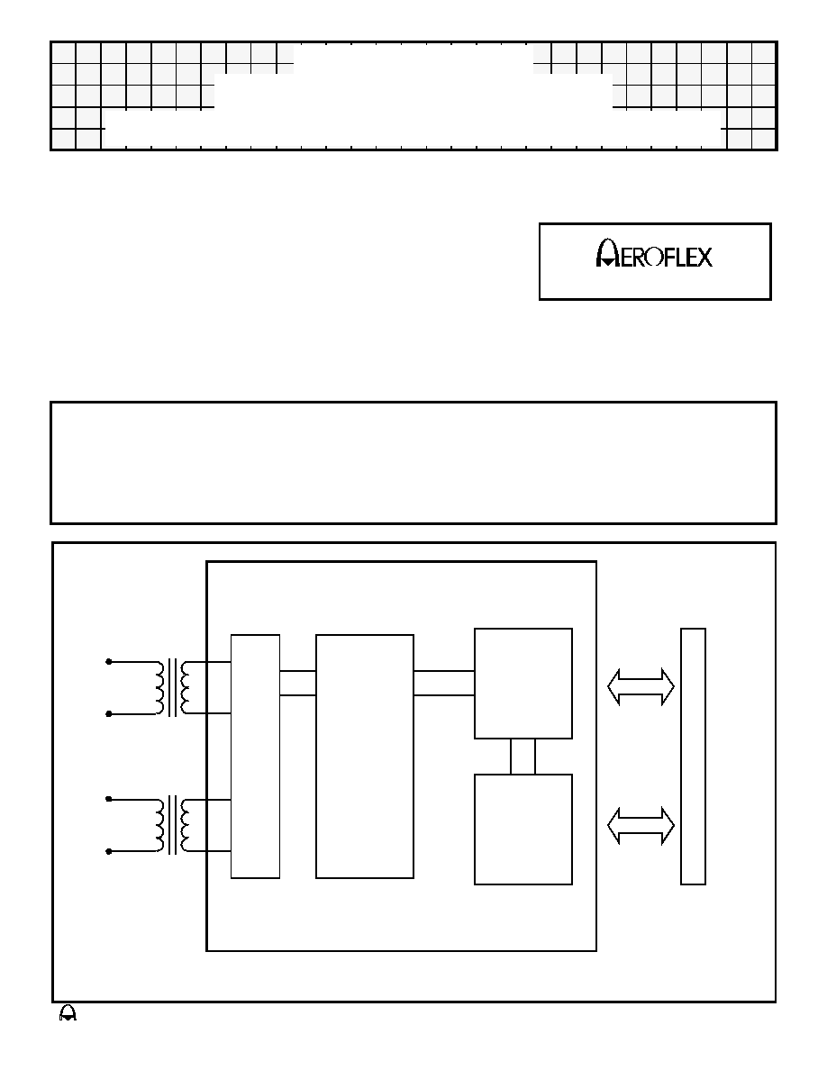
Block Diagram
BUS "0"
BUS "1"
DUAL
TX/RX
1553
PROTOCOL
µP
INTERFACE
RAM
S
U
B
S
Y
S
T
E
M
ACT7005 / ACT7006
8/16
BIT
I/O
INTERRUPTS/
CONTROL
SIGNALS
CIRCUIT TECHNOLOGY
www.aeroflex.com
Dual Transceiver, Protocol, Subsystem
ACT7005/7006
Single Package Solution

Aeroflex Circuit Technology
SCD7005 REV B 8/2/01
Plainview NY (516) 694-6700
2
F
i
g
u
r
e
1
≠
F
U
N
C
T
I
O
NAL
BL
OCK DI
A
G
RAM
INT
E
RF
A
C
E
UNIT
ST
A
T
U
S
CO
NT
RO
L
SE
L
F
T
E
S
T
CIRCUIT
R
Y
INT
E
RNAL
HIG
H
W
A
Y
T
RANS
M
I
T
RAM
CO
NT
RO
L
WO
R
D
RE
CE
IV
E
RAM
1k x 16
1k x 16
RE
CE
IV
E
FI
F
O
B
U
FFE
R
32 x 16
T
RANS
M
I
T
FI
FO
B
U
FFE
R
32
x 16
OU
T
P
U
T
FI
FO
B
U
FFE
R
32
x 16
INP
U
T
FI
F
O
B
U
FFE
R
32 x 16
8
BIT
INT
E
RNAL
HIG
H
W
A
Y
ARBIT
R
A
T
IO
N
AND
CO
NT
RO
L
L
O
G
I
C
BI-
D
IRE
C
T
I
O
NAL
I/O
D
A
T
A
BUF
F
E
R
8
o
r
1
6
B
I
T
SY
ST
EM
S
B
U
S
HANDS
HAKE
a
n
d
CO
NT
RO
L
S
I
G
NAL
S
O
p
er
at
io
n
R
e
g
i
st
er
S
y
n
c
/S
t
a
t
W
D
#2/R
M
D
R
e
g
i
st
er
S
t
at
u
s
W
o
r
d
#
1
R
e
g
i
st
e
r
R
ece
ive C
o
m
m
an
d
R
e
g
i
st
er
R
T
Co
m
m
a
n
d
W
o
r
d
Re
g
i
s
t
e
r
C
o
m
m
a
n
d
W
o
r
d
#1 R
e
g
i
st
er
V
W
/CMD W
o
r
d
#2
/AMD Reg
i
st
e
r
C
o
ntr
o
l
S
i
gn
a
l
s
a
n
d I
n
te
r
r
upts
ADDRE
S
S
DIS
CRE
T
E
INP
U
T
/
O
U
T
P
UT
S
I
G
NAL
S
E
NCO
DE
R
DE
CO
DE
R "
0
"
DE
CO
DE
R "
1
"
Dr
iv
e
r
S
e
lect
an
d
En
a
b
l
e
MU
X
MU
X
MU
X
T
r
an
sceiver
"0"
T
r
an
sceiver
"1"
BUS
"
0
"
BUS
"
1
"
Te
r
m
i
n
a
l
A
ddr
e
s
s
I
nput
s

Aeroflex Circuit Technology
SCD7005 REV B 8/2/01
Plainview NY (516) 694-6700
3
Parameter
Min
Max
Units
Power Supply Voltage (V
CC
)
-0.3
7.0
V
Power Supply Voltage (V
CCL
& V
DD
)
-0.3
7.0
V
Receiver Differential Input
(DATA CH A/B / DATA CH A/B)
-10
+10
V
Receiver Input Voltage
(DATA CH A/B or DATA CH A/B ≠ Common Mode)
-5
+5
V
Operating Case Temperature Range (T
C
)
-55
+125
∞C
Transmission Duty Cycle at T
C
= +125∞C
-
100
%
Table 1 ≠ Absolute Maximum Ratings
Parameter/Condition
Symbol
Min
Typ
Max
Unit
Power Supply Voltage
V
CC
4.75
5
5.5
mA
Total supply current "standby" mode or transmitting at
less than 1% duty cycle (e.g. 20µs of transmission every
2ms or longer interval). 2/
I
CC
@1
%
18
30
mA
Total supply current transmitting at 1MHz into a 35
load
at Point A in Figure 1. 2/ 1/
I
CC
@
25%
I
CC
@
50%
I
CC
@
100%
150
300
600
175
350
700
mA
mA
mA
Note:
1/
Decreases linearly to applicable "standyby" values at zero duty cycle.
2/
Represents one channel only.
Table 2 ≠ Analog Transceiver Power Supply Characteristics

Aeroflex Circuit Technology
SCD7005 REV B 8/2/01
Plainview NY (516) 694-6700
4
Parameter/Condition
Symbol
Min
Max
Unit
Differential impedance DC to 1MHz,
See Figure 4
Point A
Z
IO
2K
Point C
1K
Differential voltage range
V
DIR
-10
+10
V
PEAK
Input common mode voltage range
V
ICR
-5
+5
V
PEAK
Common mode rejection ratio (from point A, Figure 4)
CMRR
40
dB
Threshold characteristics (sine wave at 1MHz)
NOTE: Threshold voltages refer Figure 4
Point A
V
TH
1
0.8
1.1
Vp-p
Point C
V
TH
2
0.56
0.86
Vp-p
Table 3 ≠ Analog Transceiver Electrical Characteristics (Receiver Section)
(Over Full Temperature Range)
Parameter / Condition
Symbol
Min
Typ
Max
Unit
Differential output level at point B,
See Figure 4
140
Point B
V
O
24
35
Vp-p
70
Point C
18
25
Vp-p
Differential Output Noise at Point A, See Figure 4
V
NOI
10
mVp-p
Output Offset at point A in Figure 4,
2.5µs after mid-bit crossing of parity bit
of last word of a 660µs message
Point A (35
)
Vos
1
-90
+90
mV
Point C (70
)
Vos
2
-250
+250
mV
Rise and Fall times (10% to 90% of p-p output)
t
R
&
t
F
100
160
300
ns
Table 4 ≠ Analog Transceiver Electrical Characteristics (Transmitter Section)
(Over Full Temperature Range)

Aeroflex Circuit Technology
SCD7005 REV B 8/2/01
Plainview NY (516) 694-6700
5
Symbol
Parameter
Min
Typ
Max
Units
Conditions
V
DD
Logic Supply
4.5
5.0
5.5
VDC
V
IH
Input "1"
2.4
V
V
IL
Input "0"
0.6
V
I
L
Input I
-450
-600
-900
µA
Note 1A
I
IH
Input I
-250
-400
-750
µA
Note 1B
I
L
Input I
-50
-200
-800
µA
Note 1C
I
IH
Input I
-50
-200
-800
µA
Note 1D
I
L
Input I
-25
-125
-400
µA
Note 2A
I
IH
Input I
-25
-125
-400
µA
Note 2B
V
OH
Output "1"
2.4
VDC
Note 3A
V
OL
Output "0"
0.4
VDC
Note 3B
V
DD
Static I
50
mA
Note 4A
V
DD
Dynamic I
170
mA
Note 4B
Notes:
1.
V
DD
= 5.5V
A. For RTAD0/1/2/3/4 and RTADPAR with VIL = 0.4V
B. For RTAD0/1/2/3/4 and RTADPAR with VIH = 2.4V
C. FOR BCSTEN WITH VIL = 0.4V, Test 1, 6MHz
D. FOR BCSTEN WITH VIH = 2.4V, Test 1, 6MHz
2.
All remaining inputs and I/O
VDD = 5.5V
A. VIL = 0.4V
B. VIH = 2.4V
3.
A. VDD = 4.5V and IOH = 3mA
B. VDD = 5.5V and IOL = 3mA
4.
VDD = 5.5V
A. Clock Input = 6MHz (45-55% Duty Cycle / TTL Levels), All remaining inputs = VDD,
All Outputs = Open Circuit
B. During a 32 word FIFO to RAM or RAM to FIFO block
move
.
Table 5 ≠ Logic Electrical Characteristics
(Over Full Temperature Range)