 | –≠–ª–µ–∫—Ç—Ä–æ–Ω–Ω—ã–π –∫–æ–º–ø–æ–Ω–µ–Ω—Ç: ACT4404N | –°–∫–∞—á–∞—Ç—å:  PDF PDF  ZIP ZIP |

SCD4404N Rev C
FEATURES
ACT4404N transceiver meets MIL-STD-1553A & B, Macair A3818, A4905, A5232 and A5690 specs
Bipolar supply ±15V to ±12V, logic supply +5V
Monolithic construction
Direct replacement for CT3232M
Voltage source output for higher bus drive power
Variable receiver threshold capability
Designed for commercial, industrial and aerospace applications
MIL-PRF-38534 compliant devices available
Aeroflex-Plainview is a Class H & K MIL-PRF-38534 manufacturer
GENERAL DESCRIPTION
The Aeroflex-Plainview transceiver model ACT4404N is a new generation monolithic transceiver which provide full compliance
with Macair and MIL-STD-1553 data bus requirements.
The model ACT4404N performs the front-end analog function of inputting and outputting data through a transformer to a
MIL-STD-1553 or Macair data bus. The ACT4404N can be considered a "Universal" Transceiver in that it is compatible with
MIL-STD-1553A/B, Macair (A-3818, A-4905, A-5232 and A-5690).
Design of these transceivers reflects particular attention to active filter performance. This results in low bit and word error rate
with superior waveform purity and minimal zero crossover distortion. The ACT4404N active filter design has additional high
frequency roll-off to provide the required Macair low harmonic distortion waveform without increasing the pulse delay
characteristics significantly.
Efficient transmitter electrical and thermal design provides low internal power dissipation and heat rise at high and well as low
duty cycles. An optional receiver input threshold adjustment can be accomplished by the use of the ''External Threshold"
terminals.
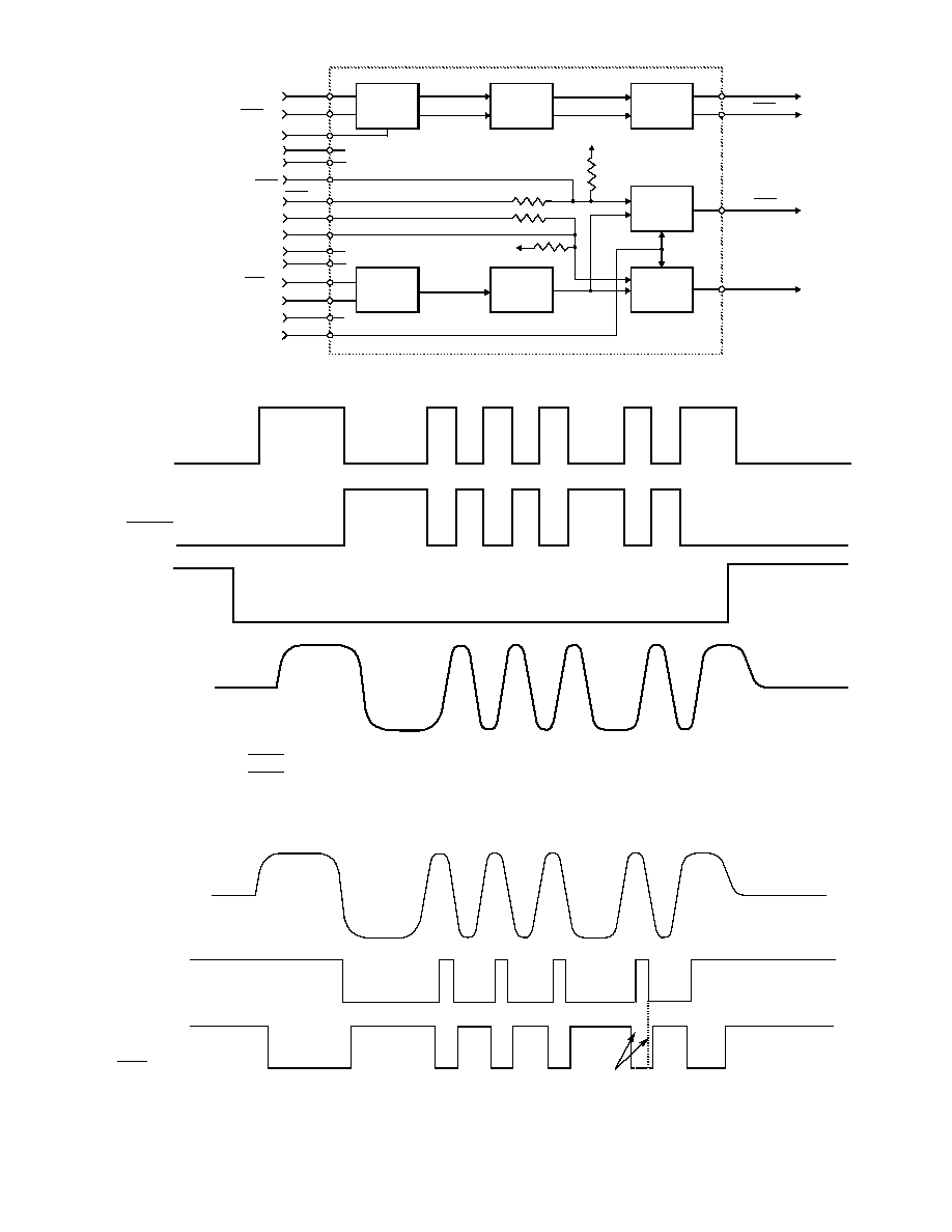
TRANSMITTER
The Transmitter section accepts bi-phase TTL data at the input and when coupled to the data bus with a 1:1 transformer the data
bus signal produced is 7.0 Volts typical P-P at point A-A' (See Figure 3 or 4). When both DATA and DATA inputs are held low or
high, the transmitter output becomes a high impedance and is "removed" from the line. In addition, an overriding "INHIBIT''
input provides for the removal of the transmitter output from the line. A logic '' 1'' applied to the '' INHIBIT'' takes priority over
the condition of the data inputs and disables the transmitter (See Transmitter Logic Waveforms - Figure 1).
The transmitter utilizes an active filter to suppress harmonics above 1 MHz to meet Macair specifications A-3818, A-4905,
A-5232 and A-5690. The transmitter may be safely operated for an indefinite period at 100% duty cycle into a data bus short
circuit.
The transceiver utilizes an active filter to suppress harmonics above 1MHz. The Transmitter may be safely operated at 100%
duty cycle for an indefinite period into a short circuited 1553 bus.
RECEIVER
The Receiver section accepts bi-phase differential data at the input and produces two TTL signals at the output. The outputs are
DATA and DATA, and represent positive and negative excursions of the input beyond a pre-determined threshold (See Receiver
Logic Waveforms - Figure 2).
The internal threshold is nominally set to detect data bus signals exceeding 1.05 Vp-p and reject signals less than 0.6 Vp-p when
used with a 1:1 turns ratio transformer (See Figure 3 or 4 for transformer data and typical connection). This threshold setting can
be held by grounding the appropriate pins or modified with the use of external resistors.
A low level at the ''STROBE'' input inhibits the DATA and DATA outputs. If unused, a 2K Ohm pull-up to +5V
DC
is
recommended.
ACT4404N Single Transceiver
Standard Products
www.aeroflex.com/Avionics
March 4, 2005
for MACAIR (A3818, A4905, A5232, A5690), MIL-STD-1553
& SAE-AS15531
2
SCD4404N Rev C
FIGURE 1 ≠ TRANSMITTER LOGIC WAVEFORMS IDEALIZED
FIGURE 2 ≠ RECEIVER LOGIC WAVEFORMS IDEALIZED
DATA IN
DATA IN
INHIBIT
LINE TO LINE
OUTPUT
Notes:
2. DATA and DATA inputs must be complementary waveforms or 50% duty cycle average, with no delays between them.
3. DATA and DATA must be in the same state during off time (both high or low).
1. Line to line waveforms illustrate Macair signals, MIL-STD-1553 signals are trapezoidal.
Note overlap
LINE TO LINE
INPUT
DATA OUT
DATA OUT
1. Normally high output in standby.
Notes:
SHAPING
OUTPUT
STAGE
COMP.
COMP.
ACTIVE
FILTER
INPUT
AMP
DRIVER
TX DATA IN
TX DATA IN
TX INHIBIT
+5 V
RX DATA IN
RX DATA IN
STROBE
TX DATA OUT
TX DATA OUT
RX DATA OUT
RX DATA OUT
-12V or -15V
EXT. THRESHOLD
DATA
SET INTERNAL
DATA
DATA
EXT. THRESHOLD
DATA
+15V or +12V
V+
V-
THRESHOLD
GND
CASE GND
BLOCK DIAGRAM (WITHOUT TRANSFORMER
SCD4404N Rev C
3
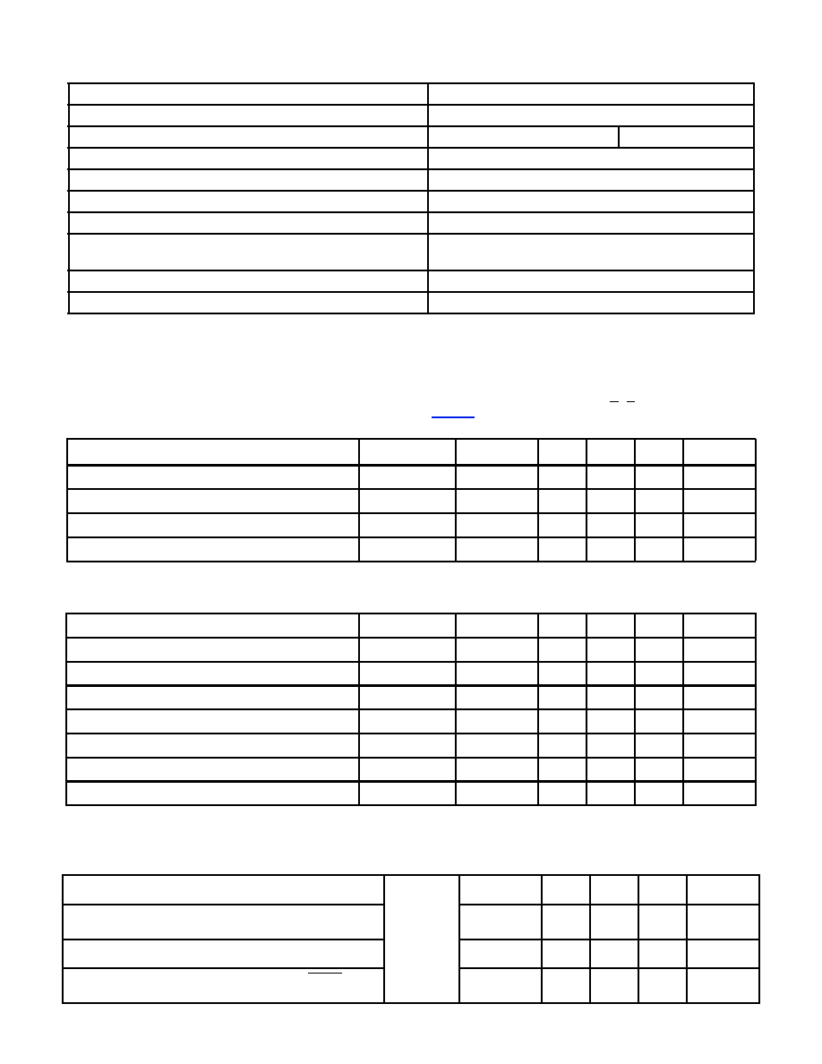
ABSOLUTE MAXIMUM RATINGS
Operating Case Temperature
-55∞C to +125∞C
Storage Case Temperature
-65∞C to +150∞C
Power Supply Voltages
±15V
DC
to ±18V
DC
+5V
DC
to +7V
DC
Logic Input Voltage
-0.3 V to +5.5 V
Receiver Differential Input
±40 V
Receiver Input Voltage (Common Mode)
±10V
Driver Peak Output Current
150 mA
Total Package Power Dissipation over the Full Operating Case
Temperature Range
*
3.25 Watts
Maximum Junction to Case Temperature (100% duty cycle)
16.25∞C
Junction-Case, Thermal Resistance
5∞C/W
*
See Aeroflex Application Note # 112 for reference.
ELECTRICAL CHARACTERISTICS ≠ DRIVER SECTION
1/ 2/
INPUT CHARACTERISTICS, TX DATA IN OR TX DATA IN
Parameter
Condition
Symbol
Min
Typ
Max
Unit
"0" Input Current
V
IN
= 0.4V
I
ILD
-
-0.2
-0.4
mA
"1" Input Current
V
IN
= 2.7V
I
IHD
-
1
40
µA
"0" Input Voltage
-
V
ILD
-
-
0.7
V
"1" Input Voltage
-
V
IHD
2.0
-
-
V
INHIBIT CHARACTERISTICS
"0" Input Current
V
IN
= 0.4V
I
ILI
-
-0.1
-0.2
mA
"1" Input Current
V
IN
= 2.7V
I
IHI
-
1.0
40
µA
"0" Input Voltage
-
V
ILI
-
-
0.7
V
"1" Input Voltage
-
V
IHI
2
-
-
V
Delay from TX inhibit, (0
1) to inhibited output
Note 1
t
DXOFF
-
350
700
nS
Delay from TX inhibit, (1
0) to active output
Note 1
t
DXON
-
300
500
nS
Differential Output Noise, inhibit mode
-
V
NOI
-
0.8
10
mVp-p
Differential Output Impedance (inhibited) *
Note 2
Z
OI
10K
-
-
*
See Aeroflex Application Note # 113 for reference.
OUTPUT CHARACTERISTICS
Differential output Level, Figure 3 Point B-B'
Z
O
= 70
V
O
18
21
24
Vp-p
Output offset at point A-A on Figures 3 or 4, 2.5µS after
midpoint crossing of the last bit
V
OS
-
-
±90
mVpeak
Output rise / fall times (10% to 90% of p-p output)
t
R
& t
F
200
250
300
nS
Delay from 50% point of TX DATA or TX DATA input
to zero crossing of differential output (Note 1)
t
DTX
-
220
350
nS

4
SCD4404N Rev C
ELECTRICAL CHARACTERISTICS ≠ RECEIVER SECTION
1/ 2
/
Parameter
Condition
Symbol
Min
Typ
Max
Unit
Differential Input Impedance
f = 1MHz
Z
IN
10K
-
-
Differential Input Voltage Range
-
V
IDR
-
-
40
Vp-p
Input Common Mode Voltage Range
-
V
ICR
10
-
-
Vp-p
Common Mode Rejection Ratio
-
CMRR
40
-
-
dB
STROBE CHARACTERISTICS (LOGIC "0" INHIBITS OUTPUT)
"0" Input Current
V
S
= 0.4V
I
IL
-
-0.2
-0.4
mA
"1" Input Current
V
S
= 2.7V
I
IH
-
1
+40
µA
"0" Input Voltage
-
V
IL
-
-
0.7
V
"1" Input Voltage
-
V
IH
2.0
-
-
V
Strobe Delay (Turn-on or Turn-off)
-
t
SD
-
40
150
nS
THRESHOLD CHARACTERISTICS (SINEWAVE INPUT)
Internal Threshold Voltage Figure 3
Point B - B'
1MHz
V
TH
0.60
0.80
1.10
Vp-p
OUTPUT CHARACTERISTICS, RX DATA AND RX DATA
"1" State
I
OH
= -0.4 mA
V
OH
2.5
3.6
-
V
"0" State
I
OL
= 4 mA
V
OL
-
0.35
0.5
V
Receiver Output Skew
Note 6
t
RXSK
-
-
10
nS
Delay (average), from differential input zero
crossings to RX DATA and RX DATA output
50% points
Note 7
t
DRX
-
300
450
nS
POWER SUPPLY CURRENT
1/ 2/
Duty Cycle
Condition
Symbol
Typ
Max
Unit
Transmitter Standby
Point B-B', Z
O
= 70
, V
O
= 29 V
P
-
P
Bit Pattern = FFFF
HEX
Figure 4
I
CC
I
EE
I
L
5
25
18
10
35
30
mA
25%
I
CC
I
EE
I
L
20
40
18
30
60
30
50%
I
CC
I
EE
I
L
40
60
18
60
80
30
100%
I
CC
I
EE
I
L
85
105
18
120
140
30

5
SCD4404N Rev C
Notes:
1. V
CC
= +15V
DC
±0.75V, V
EE
= -151.V
CC
= +15V
DC
±0.75V, V
IL
= +5V
DC
±0.5V, T
C
= -55∞C to +125∞C, unless otherwise specified.
2. All typical values are measured at +25∞C.
3. Characteristics guaranteed by design, not production tested.
4. Power ON/OFF, measured from 75KHz to 1MHz at Point A-A' Figure 4, in accordance with MIL-STD-1553B paragraph 4.5.2.2.2.3.
5. At point A-A' on Figure 3 or 4, 2.5µS after midpoint crossing of the parity bit of the last word of a 660 µS message.
6. Receiver skew is defined as the time from the rising edge of RX DATA OUT to the rising edge of RX DATA OUT minus 500 nS, with a sine
wave input of 3 V
P
-
P
at 1MHz driven into Point B-B' of Figure 4 or 2.1 V
P
-
P
at 1MHz driven into Point B-B' of Figure 3. The specification
maximum is guaranteed for T
A
= 25∞C only. Standard TTL loads applied to RX DATA Outputs.
7. This test is performed while the Transceiver is reading its own transmission. This condition is called "Wraparound". Standard TTL loads
applied to RX DATA Outputs.
TYPICAL HYBRID POWER DISSIPATION
*
Power Supply Conditions
Condition
Standby
100% Duty
Cycle
Unit
PSC1
V
CC
= +15V
V
EE
= -15V
V
L
= +5V
Point B-B', Z
O
= 70
, V
O
= 29 V
P
-
P
Bit Pattern = FFFF
HEX
Figure 4
0.540
2.167
Watts
PSC2
V
CC
= +15V
V
EE
= -12V
V
L
= +5V
0.465
1.852
PSC3
V
CC
= +12V
V
EE
= -12V
V
L
= +5V
0.450
1.600
*
See Aeroflex Application note# 112 for reference.
Recommended Power Supply Voltage Range
+V
+11.4 Volts to +15.75 Volts
-V
-11.4 Volts to -15.75 Volts
Logic
+4.5 Volts to +5.5 Volts