SCD4435N Rev B
ACT 4435NFP
AEROFLEX
ACT 4435N
USA-88379
AEROFLEX
USA-88379
FEATURES
ACT4435N Transceiver meets H009 data bus specifications
Transmitter can be used to drive clock signal line
Operates with �15 Volts to �12 Volts power supplies
Direct replacement for CT1641 and CT1816 devices
Voltage source output for higher bus drive power
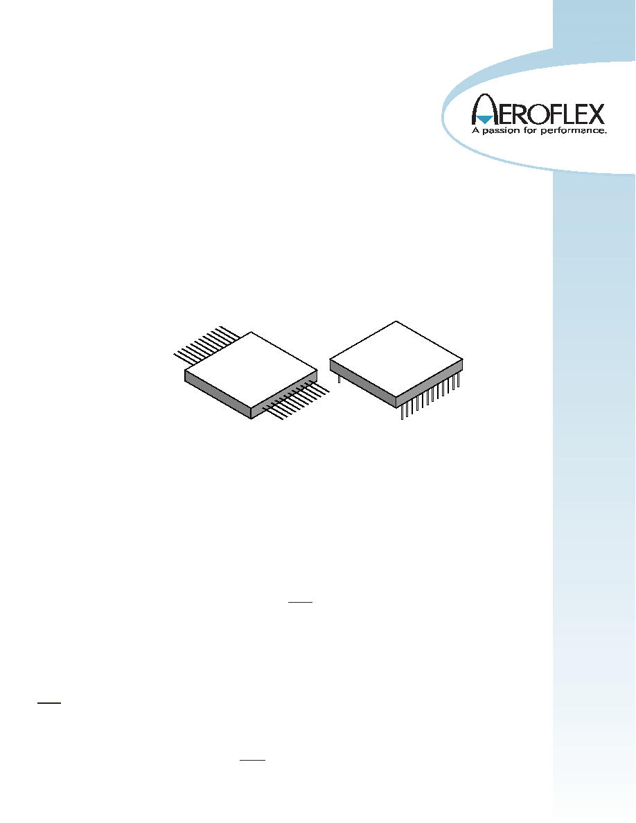
Plug-in and flat package available
Monolithic construction using linear ASICs
Processed and screened to MIL-STD-883 specs
MIL-PRF-38534 compliant devices available
Aeroflex is a Class H & K MIL-PRF-38534 Manufacturer
GENERAL DESCRIPTION
The Aeroflex Laboratories transceiver model ACT4435N is a new generation monolithic transceiver which provide full compliance with
Macair and MIL-STD-1553 data bus requirements
The model ACT 4435N performs the front-end analog function of inputting and outputting data through a transformer to a H009 data bus.
The Design of these transceivers reflects particular attention to active filter performance. This results in low bit and word error rate with
superior waveform purity and minimal zero crossover distortion. The ACT 4435N active filter design has additional high frequency roll-off to
provide the required low harmonic distortion waveform without increasing the pulse delay characteristics significantly.
Efficient transmitter electrical and thermal design provides low internal power dissipation and heat rise at high and well as low duty cycles.
An optional receiver input threshold adjustment can be accomplished by the use of the "External Threshold" terminals.
TRANSMITTER
The Transmitter section accepts bi-phase TTL data at the input and when coupled to the data bus with a 1:1 transformer, isolated on the
transceiver side with two 35 Ohm bus terminating resistors, with the bus terminated by a 170 Ohm resistor the data bus signal produced is 20.0
Volts typical P-P at A-A' (See Figure 5). When both DATA and DATA inputs are held low or high, the transmitter output becomes a low
impedance and signal is "removed" from the line. In addition, an overriding "INHIBIT" input returns the output to a high impedance state. A
logic "1" applied to the "INHIBIT" takes priority over the condition of the data inputs and disables the transmitter (See Transmitter Logic
Waveforms - Figure 1).
The transmitter utilizes an active filter to suppress harmonics above 1 MHz to meet H009 specifications. The transmitter may be safely operated
for an indefinite period at 100% duty cycle into a data bus short circuit.
RECEIVER
The Receiver section accepts bi-phase differential data at the input and produces two TTL signals at the output. The outputs are DATA and
DATA, and represent positive and negative excursions of the input beyond a pre-determined threshold (See Receiver Logic Waveforms -
Figure 2).
The internal threshold is nominally set to detect data bus signals exceeding 1.05 Volts P-P and reject signals less than 0.6 Volts P-P when used
with a 1:1 turns ratio transformer (See Figure 5 for transformer data and typical connection). This threshold setting can be held by grounding
the appropriate pins or modified with the use of external resistors.
A low level at the Strobe input inhibits the DATA and DATA outputs. If unused, a 2K Ohm pull-up to +5 Volts is recommended.
ACT4435N Transceiver
Standard Products
for H009 Specification
June 18, 2004
ACT4435NFP / 4435N

2
SCD4435N Rev B
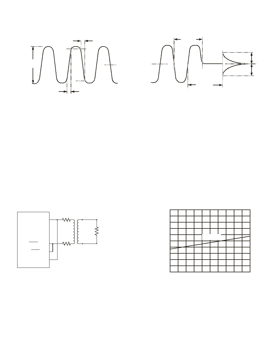
FIGURE 1 � TRANSMITTER LOGIC WAVEFORMS
FIGURE 2 � RECEIVER LOGIC WAVEFORMS
DATA IN
DATA IN
INHIBIT
LINE TO LINE
OUTPUT
Notes: 1. Data and DATA inputs must be complementry waveforms or 50% duty cycle average, with no delays between them, and in the same state during
the off time (both high and low).
2. Region 1 ; no output signal, High Z state, (Receive Mode), Region 2; No Output signal, Low Z state, (Terminate Mode), Region 3, Transmitter signal
on, low Z.
Region 1 2 3
Note overlap
Note
:
Waveforms shown are for normally low devices. For normally high receiver output
devices, the receiver outputs are swapped as shown by the dashed lines
level
LINE TO LINE
INPUT
Rx DATA OUT
Rx DATA OUT
BLOCK DIAGRAM (WITHOUT TRANSFORMER)
SHAPING
OUTPUT
STAGE
COMP.
COMP.
ACTIVE
FILTER
INPUT
AMP
DRIVER
TX DATA IN
TX DATA IN
TX INHIBIT
+5 V
RX DATA IN
RX DATA IN
STROBE
TX DATA OUT
TX DATA OUT
RX DATA OUT
RX DATA OUT
-12V or -15V
EXT. THRESHOLD
DATA
SET INTERNAL
DATA
DATA
EXT. THRESHOLD
DATA
+15V or +12V
V+
V-
THRESHOLD

SCD4435N Rev B
3
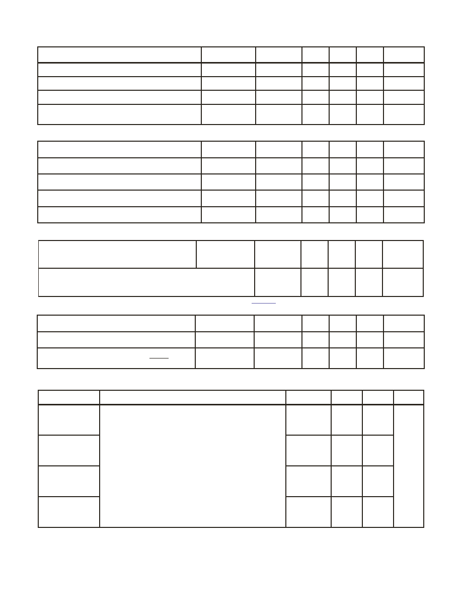
ABSOLUTE MAXIMUM RATINGS
Operating Case Temperature
-55�C to +125�C
Storage Case Temperature
-65�C to +150�C
Power Supply Voltages
�15V
DC
P.S. to �18V
DC
MAX
+5V
DC
P.S. to +7V
DC
Logic Input Voltage
-0.3 V to +5.5 V
Receiver Differential Input
�40 V
Receiver Input Voltage (Common Mode)
�10V
Driver Peak Output Current
150 mA
Total Package Power Dissipation over the Full Operating
Case Temperature Range
3.25 Watts
Maximum Junction to Case Temperature (100% duty cycle)
16.25�C
Junction-Case, Thermal Resistance
5�C/W
ELECTRICAL CHARACTERISTICS � DRIVER SECTION
INPUT CHARACTERISTICS, TX DATA IN OR TX DATA IN
Parameter
Condition
Symbol
Min
Typ
Max
Unit
"0" Input Current
V
IN
= 0.4V
I
ILD
-
-0.2
-0.4
mA
"1" Input Current
V
IN
= 2.7V
I
IHD
-
1
40
�A
"0" Input Voltage
V
ILD
-
-
0.7
V
"1" Input Voltage
V
IHD
2.0
-
-
V
INHIBIT CHARACTERISTICS
"0" Input Current
V
IN
= 0.4V
I
ILI
-
-0.2
-0.4
mA
"1" Input Current
V
IN
= 2.7V
I
IHI
-
1.0
40
�A
"0" Input Voltage
V
ILI
-
-
0.7
V
"1" Input Voltage
V
IHI
2
-
-
V
Delay from TX inhibit, (0
1) to inhibited output
Note 1
t
DXOFF
-
200
500
nS
Delay from TX inhibit, (1
0) to active output
Note 1
t
DXON
-
250
700
nS
Differential Output Noise, inhibit mode
V
NOI
-
0.8
10
mV p-p
Differential Output Impedance (inhibited)
Note2 Z
OI
10K
-
-
OUTPUT CHARACTERISTICS
Differential output level at point A-A' on
Figure 5
R
L
=170
V
O
17
21
24
V p-p
Rise and fall times
(10% to 90% of p-p output)
t
r
200
-
300
nS
Output offset at point A-A' on Figure 5, 2.5 �S
after midpoint crossing of the last bit
R
L
=170
V
OS
-
-
�265
mV peak
Delay from 50% point of TX DATA or
TX DATA input to zero crossing of differential
signal (Note 1)
t
DTX
-
270
400
nS
SCD4435N Rev B
4
Notes:
1. Characteristics guaranteed by design, not production tested.
2. Measured at 1mHz at point A-A', power on or off.
3. Specifications apply over the temperature range of -55�C to +125�C (case temperature) unless otherwise noted.
4. All typical values are measured at +25�C.
ELECTRICAL CHARACTERISTICS � RECEIVER SECTION
Parameter
Condition
Symbol
Min
Typ
Max
Unit
Differential Input Impedance (Note 1)
f= 1MHz
Z
IN
20K
-
-
Differential Input Voltage Range
V
IDR
-
-
40 V
p-p
Input Common Mode Voltage Range
Note 1
V
ICR
10
-
-
V p-p
Common Mode Rejection Ratio
Point A-A on
Figure 5
CMRR
40
-
-
dB
STROBE CHARACTERISTICS (LOGIC "0" INHIBITS OUTPUT)
"0" Input Current
V
S
= 0.4V
I
IL
-
-0.2
-0.4
mA
"1" Input Current
V
S
= 2.7V
I
IH
-
1
+40
�A
"0" Input Voltage
V
IL
-
-
0.7
V
"1" Input Voltage
V
IH
2.0
-
-
V
Strobe Delay (turn-on or turn-off)
t
SD(ON)
-
-
150
nS
THRESHOLD CHARACTERISTICS (SINEWAVE INPUT )
Internal Threshold Voltage
(Referred to the bus) Pins 6 and 11 to GND
For 4435N-701 only � Pins 6 and 11 to GND
100KHz-1MHz
V
TH
0.60
1.2
0.80
1.8
1.15
2.3
V P-P
V P-P
External Threshold
Pins 6 & 11 open, threshold settings resistors from Pin 5 & 12 to
ground; For R
TH
= 3K mimumn to 10K maximum
R
TH
/V
TH1
-
4000
-
/
V
P-P
OUTPUT CHARACTERISTICS, RX DATA AND RX DATA
"1" State
I
OH
= -0.4mA
V
OH
2.5
3.6
-
V
"0" State
I
OL
= 4mA
V
OL
-
0.35
0.5
V
Delay, (average) from differential input zero
crossings to RX DATA and RX DATA output
50% points
t
DRX
-
275
450
nS
POWER SUPPLY CURRENT
Duty Cycle
Condition
Symbol
Typ
Max
Unit
Transmitter
Standby
I
CC
I
EE
I
L
5
15
18
10
35
30
mA
25%
I
CC
I
EE
I
L
25
35
18
40
60
30
50%
I
CC
I
EE
I
L
45
55
18
60
80
30
100%
I
CC
I
EE
I
L
85
95
18
120
140
30
SCD4435N Rev B
5
FIGURE 3 � TRANSMITTER (TX) OUTPUT
FIGURE 4 � TRANSMITTER (TX) OUTPUT
FIGURE 5 � TYPICAL TRANSFORMER
17V P-P MIN
24V P-P MAX
90%
10%
t
r
*
t
f
*
* Rise and fall times measured at point A-A' in Fig 5
0 Volts
OUTPUT OFFSET
*
OUTPUT OFFSET
*
LAST BIT
2.5 �sec
*Offset measured at point A-A' in Fig 5
0 Volts
Magnified View
FIGURE 6 � POWER DISSIPATION VS.
CONNECTION
WAVEFORM
OFFSET
DUTY CYCLE
N1:N2
A
A'
TX DATA OUT
TX DATA OUT
RX DATA IN
RX DATA IN
35
35
Transformer turns ratio:
N1:N2 = 1:1
Use Aeroflex 25T1553-1
170
0 10 20 30 40 50 60 70 80 90 100
4.0
3.5
3.0
2.5
2.0
1.5
1.0
0.5
0
DUTY CYCLE, PERCENT
P
O
W
E
R DI
S
S
I
P
A
T
I
O
N
W
A
T
T
S
(TYPICAL)