 | –≠–ª–µ–∫—Ç—Ä–æ–Ω–Ω—ã–π –∫–æ–º–ø–æ–Ω–µ–Ω—Ç: ACT4469DI | –°–∫–∞—á–∞—Ç—å:  PDF PDF  ZIP ZIP |

CIRCUIT TECHNOLOGY
www.aeroflex.com
eroflex Circuit T
echnology
≠ Data Bus Modules For The Future © SCD4469D REV A 5/21/01
General Description
The Aeroflex Circuit
Technology model ACT4469D is a
next generation monolithic
transceiver which provides variable
amplitude in compliance with H009
data bus requirements with the
lowest standby power consumption
available using three DC power
supplies operation.
The dual channel model
ACT4469D performs the front-end
analog function of inputting and
outputting data through a
transformer to a H009 data bus.
Design of this transceiver
reflects particular attention to active
filter performance. This results in
low bit and word error rate with
superior waveform purity and
minimal zero crossover distortion.
The ACT4469D series active filter
design provides the required H009
low harmonic distortion waveform
without increasing the pulse delay
characteristics significantly.
Efficient transmitter electrical
and thermal design provides low
internal power dissipation and heat
rise at high and well as low duty
cycles.The receiver input threshold
is set internally.
Variable amplitude is adjusted
with factory preset 0≠10Vdc control
line at 2 mA maximum input current
at 10 Volts.
Transmitter
The Transmitter section
accepts complementary TTL data
at the input, and when coupled to
the data bus with a 1:1 transformer,
isolated on the transceiver side with
two 34 ohm fault isolation resistors,
and loaded by a 175 ohm
termination, the data bus signal
produced is 20 Volts nominal P-P at
Block Diagram (without Transformer, Channel A shown)
ACTIVE
AMPLITUDE
STAGE
COMP.
COMP.
REFERENCE
ACTIVE
FILTER
DRIVER
TX DATA IN
TX DATA IN
TX INHIBIT
+5 V
STROBE
TX/RX
TX/RX
RX DATA OUT
RX DATA OUT
GROUND
V
CONT
CHANNEL B
INPUT
AMP
Channel A
Channel B
FILTER
OUTPUT
VARIABLE
TRANSMIT
RECEIVE
+V
CC
-V
EE
Channel A
Features
∑ World's smallest and lowest standby power dual
variable amplitude H009 transceiver 1.25" x 0.61"
maximum ceramic package
∑ Dual transceiver with variable output amplitude
control meets McDonnell Douglas H009 data bus
specifications
∑ Lowest standby power
∑ Low power dissipation at full output power
∑ Operates with ±12V to ±15 and +5V power supplies
∑ Voltage source output for transmitter
∑ Monolithic construction
∑ Processed to commercial or screened to
MIL-STD-883 specs
∑ +10V Control line for transmitter amplitude
adjustment (See Figure 3)
∑ Packaging ≠ Hermetic Ceramic
Non-conductive mounting surface
No package glass beads
Small size & light weight
for H009
Dual Variable Amplitude Transceivers
ACT4469D
Aeroflex Circuit Technology
SCD4469D REV A 5/21/01 Plainview NY (516) 694-6700
2
A-A' (See Figure 5). When both
DATA and DATA inputs are held low
or high, the transmitter output
impedance is low, and signal is
"removed" from the line. In
addition, an overriding "INHIBIT"
input returns the output impedance
to a high state. A logic "1" applied
to the "INHIBIT" takes priority over
the condition of the data inputs and
disables the transmitter. (See
Transmitter Logic Waveforms,
Figure 1).
The transmitter utilizes an
active filter to suppress harmonics
above 1MHz to meet H009
specification. The transmitter may
be safely operated for an indefinite
period with the output short
circuited at 100% duty cycle.
Receiver
The Receiver section accepts
bi-phase differential data at the
input and produces two TTL
signals at the output. The outputs
are DATA and DATA, and represent
positive and negative excursions of
the input beyond a pre-determined
threshold (See Receiver Logic
Waveforms, Figure 2).
The internal threshold is
nominally set to detect data bus
signals exceeding 1.0 Volts P-P
when used with a 1:1 turns ratio
transformer (See Figure 5 for
transformer data and typical
connection).
A low level at the Strobe input
inhibits the DATA and DATA
outputs. The strobe is internally
pulled up, therefore a pull resistor
is not needed.
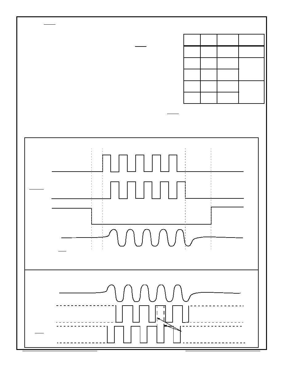
Figure 1A ≠ Tx Output Truth Table
DATA
DATA
INHIBIT
OUTPUT
X
X
H
High Z
H
H
L
Low Z
(No signal)
L
L
L
H
L
L
Low Z
(Signal)
L
H
L
DATA IN
DATA IN
INHIBIT
LINE TO LINE
OUTPUT
Figure 1B - Transmitter Logic Waveforms
Figure 2 - Receiver Logic Waveforms
Note overlap
LINE TO LINE
INPUT
Rx DATA OUT
Rx DATA OUT
Notes: 1. Data and DATA inputs must be complementary waveforms or 50% duty cycle average, with no delays between them, and in the same state during
the off time (both high and low).
2. Region 1; no output signal, High Z state, (Receive Mode), Region 2; No Output signal, Low Z state, Region 3; Transmitter signal
on, low Z (Transmitter mode), Region 4; No Output signal, Low Z state, (Terminate Mode).
Region 1 2
3
4
1

Aeroflex Circuit Technology
SCD4469D REV A 5/21/01 Plainview NY (516) 694-6700
3
Absolute Maximum Ratings, Per Channel
Operating Case Temperature
-55∞C to +125∞C
Storage Case Temperature
-65∞C to +150∞C
Power Supply Voltages
±16 V
+7 V
Logic Input Voltage
-0.3 V to +5.5 V
Receiver Differential Input
±40 V
Receiver Input Voltage (Common Mode)
±10V
Driver Peak Output Current
150 mA
Total Package Power Dissipation over the Full Operating
Case Temperature Range
3.6 Watts
Maximum Junction to Case Temperature
18∞C
Junction-Case, Thermal Resistance
5∞C/W
Electrical Characteristics ≠ Driver Section
1/ 2/
Input Characteristics, TX DATA IN or TX DATA IN
Parameter
Condition
Symbol
Min
Typ
Max
Unit
"0" Input Current
V
IN
= 0.4 V
I
ILD
-
-0.2
-0.4
mA
"1" Input Current
V
IN
= 2.7 V
I
IHD
-
1
40
µA
"0" Input Voltage
-
V
ILD
-
-
0.7
V
"1" Input Voltage
-
V
IHD
2.0
-
-
V
Inhibit Characteristics
"0" Input Current
V
IN
= 0.4V
I
ILI
-
-0.2
-0.4
mA
"1" Input Current
V
IN
= 2.7V
I
IHI
-
1.0
40
µA
"0" Input Voltage
-
V
ILI
-
-
0.7
V
"1" Input Voltage
-
V
IHI
2
-
-
V
Delay from TX inhibit,(0
1) to inhibited output
-
t
DXOFF
-
300
500
nS
Delay from TX inhibit, (1
0) to active output
-
t
DXON
-
200
400
nS
Differential Output Noise, inhibit mode
-
V
NOI
-
2
10
mVp-p
Output Characteristics
Differential output level (175
)
Pt. A - A'
V
O
16
20
24
V p-p
Rise and Fall times
-
t
R
& t
F
200
260
300
nS
Output Offset
Pt. A - A'
V
OS
-
-
±260
mV peak
Delay from 50% point of TX DATA or TX DATA
input to zero crossing of differential signal
-
t
DTX
-
280
400
nS
Control Line Input Resistance 3/
-
R
CONT
5
-
-
K

Aeroflex Circuit Technology
SCD4469D REV A 5/21/01 Plainview NY (516) 694-6700
4
Notes:
1. V
CC
= +15Volts ±0.75V, V
EE
= -15Volts ±0.75V, V
IL
= +5Volts ±0.5V, Tc = -55∞C to +125∞C, unless otherwise specified.
2. All typical values are measured at +25∞C.
3. Characteristics guaranteed by design, not production tested.
4. Power ON/OFF, measured 1MHz at Point A-A' Figure 4.
5. At point A-A' on Figure 4 or 5, 2.5 µS after midpoint crossing of the parity bit of the last word.
6. This test is peformed while the Transceiver is reading its own transmission. This condition is called "Wraparound". Standard TTL
loads applied to RX DATA Outputs.
Electrical Characteristics ≠ Receiver Section
1/
2/
Parameter
Condition
Symbol
Min
Typ
Max
Unit
Differential Voltage Range 3/
Pt. A - A'
V
IDR
-
20
V peak
Common Mode Rejection Ratio 3/
-
CMRR
45
-
-
dB
Strobe Characteristics (Logic "0" inhibits output)
(NOTE: I
f not used, a 1K pullup to 5V is recommended)
"0" Input Current
V
S
= 0.4 V
I
IL
-
-0.2
-0.4
mA
"1" Input Current
V
S
= 2.7V
I
IH
-
1
+40
µA
"0" Input Voltage
-
V
IL
-
-
0.7
V
"1" Input Voltage
-
V
IH
2.0
-
-
V
Strobe Delay (turn-on)
-
t
SD
(
ON
)
-
90
150
nS
Strobe Delay (turn-off)
-
t
SD
(
OFF
)
-
90
150
nS
Threshold Characteristics (Sinewave input )
Input Threshold Voltage, Pt. A - A' Figure 5
1MHz
V
TH
1.5
2.0
3.0
Vp-p
Output Characteristics, RX DATA and RX DATA
"1" State
I
OH
= -0.4 mA
V
OH
2.5
3.6
-
V
"0" State
I
OL
= 4 mA
V
OL
-
0.35
0.5
V
Delay (average), from differential input zero
crossings to RX DATA and RX DATA output
50% points
6/
t
DRX
-
300
450
nS
Power Supply Currents Per Channel
1/ 2/
V
CC
= +12V to +15V, V
EE
= -12V to -15V, V
L
= +5V
Duty Cycle
Condition
Symbol
Typ
Max
Unit
Transmitter Standby
Pt. A - A'
Z
O
= 175
,
V
O
= 21 V
PK
-
PK
Figure 5
I
CC
I
EE
I
L
6
16
19
10
25
25
mA
25% 3/
I
CC
I
EE
I
L
26
35
19
35
45
25
50%
I
CC
I
EE
I
L
45
54
19
55
65
25
100%
I
CC
I
EE
I
L
84
92
20
120
130
25

Aeroflex Circuit Technology
SCD4469D REV A 5/21/01 Plainview NY (516) 694-6700
5
Configurations and Ordering Information
Model No.
Receiver Data level
Case
Specs.
Configuration
ACT4469D
Normally Low
DIP
H009
Dual
ACT4469DI
Normally High
Figure 4 ≠ Transmitter (TX) Output Offset
OUTPUT OFFSET
*
OUTPUT OFFSET
*
LAST BIT
2.5 µsec
*Offset measured at point A-A' in Figure 5
Magnified View
(Total hybrid with one channel transmitting
and the other in standby)
0.4FS
0.8FS
0.6FS
0.2FS
V
O
PK
-
PK
@ A≠ A'
Figure 5 ≠ Typical Transformer connection
N1:N2
A
A'
TX/RX DATA OUT
TX/RX DATA OUT
34
34
Transformer turns ratio:
N1:N2 = 1:1
Use Aeroflex 25T1553-1
175
ACT4469D, CH A
B
B'
FS
Figure 3 ≠ Typical Transmitter Output
Amplitude (Vo) vs Vcont Voltage
0 2 4 6 8 10
CONTROL VOLTAGE
OUT
P
UT
A
M
P
L
I
T
UDE
8.4
21
16.8
12.6
4.2
0
V
CONT
dc
Slope =
V
O
˜
V
CONT
Figure 6 ≠ Power Dissipation vs. Duty Cycle
P
O
W
E
R DI
S
S
I
P
A
T
I
O
N
M
I
L
L
IW
A
T
TS
Note: Vcc = ±15V Volts, V
bus
(Pt. A-A') at 21 Volts P-P
0 10 20 30 40 50 60 70 80 90 100
3.2
2.8
2.4
2.0
1.6
1.2
.8
.4
0
DUTY CYCLE ≠ PERCENT
Typical
Maximum
@175
3.6
+
+
*
*
* External Coupling Capacitors are required for each output.
Recommened 1µF ceramic 25V/50V or can use Tantalum
(15WVDC min) with 0.1µF ceramic in parallel for each output.
C
C