 | –≠–ª–µ–∫—Ç—Ä–æ–Ω–Ω—ã–π –∫–æ–º–ø–æ–Ω–µ–Ω—Ç: ACT4487-D | –°–∫–∞—á–∞—Ç—å:  PDF PDF  ZIP ZIP |

CIRCUIT TECHNOLOGY
www.aeroflex.com/act1.htm
eroflex Circuit T
echnology
≠ Data Bus Modules For The Future © SCD4487D REV B 3/10/98
General Description
The Aeroflex Circuit
Technology ACT 4487 is a next
generation monolithic transceiver
design which provides full
compliance to MIL-STD-1553A/B
and 1760 requirements in a small
package with low power
consumption.
The ACT 4487 series performs
the front-end analog function of
inputting and outputting data
through a transformer to the
MIL-STD-1553 data bus.
Design of this transceiver reflects
particular attention to active filter
performance. This results in low bit
and word error rate with superior
waveform purity and minimal zero
crossover distortion. Efficient
transmitter electrical and thermal
design provides low internal power
dissipation and heat rise at high as
well as low duty cycles.
Each channel of the dual
transceiver is completely separate
from the other and fully
independent. This includes power
leads as well as signal lines.
Hence, each channel may be
connected to a different data bus
with no interaction.
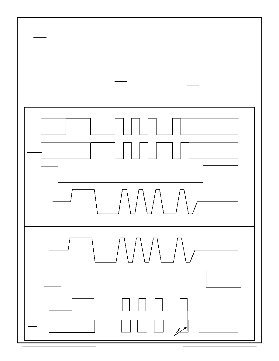
Transmitter:
The Transmitter section accepts
bi-phase TTL data at the input and
when coupled to the data bus with a
1.4:1 ratio transformer, isolated on
the data bus side with two 52.5
Ohm fault isolation resistors, and
loaded by two 70 Ohm
Block Diagram (Without Transformer)
ACTIVE
OUTPUT
STAGE
COMP.
COMP.
REFERENCE
ACTIVE
FILTER
INPUT
AMPLIFIER
DRIVER
TX DATA IN
TX DATA IN
TX INHIBIT IN
-15V (V
EE
)
RX DATA IN
RX DATA IN
RX STROBE IN
TX DATA OUT
TX DATA OUT
RX DATA OUT
RX DATA OUT
FILTER
GND3
+5V (V
L
)
GND1
+15V (V
CC
)
GND2
CASE
Features
∑ +5 / ±15 Volt Supply Operation
∑ Low Power Dissipation
∑ Small Size & Light Weight
∑ Dual Transceivers Saves Space & Cost
∑ Outstanding MIL-STD-1553 performance
∑ Radiation Hard Dielectric Isolation Monolithic
Construction for Severe Environments
∑ Superior High Frequency Line Transient and
Input Ripple Rejection
∑ Input and Output TTL Compatible Design
∑ Processed and Screened to MIL-STD-883 Specs
∑ MIL-PRF-38534 Compliant Devices Available
∑ DESC SMD (Standard Military Drawing)
ACT 4487 DUAL TRANSCEIVER
FOR MIL-STD-1553/1760
Aeroflex Circuit Technology
SCD4487D REV B 3/10/98 Plainview NY (516) 694-6700
2
terminations, the data bus signal is
typically 7.5 Volts P-P at point A
(See Figure 5). When both DATA
and DATA inputs are held low or
high, the transmitter output
becomes a high impedance and is
"removed" from the line. In addition,
an overriding "INHIBIT" input
provides for the removal of the
transmitter output from the line. A
logic "1" signal applied to the
"INHIBIT" takes priority over the
condition of the data inputs and
disables the transmitter (See
Transmitter Logic Waveform,
Figure 1). The Transmitter may be
safely operated for an indefinite
period with the bus (point A) short
circuited at 100% duty cycle.
Receiver:
The Receiver section accepts
bi-phase differential data at the
input and produces two TTL signals
at the output. The outputs are DATA
and DATA, and represent positive
and negative excursions of the input
beyond a pre-determined threshold
(See Receiver Logic Waveform,
Figure 2).
The pre-set internal thresholds
will detect data bus signals, point
A Figure 5, exceeding 1.20 Volts
P-P and reject signals less than
0.6 Volts P-P when used with a
transformer (See Figure 5 for
transformer data and typical
connection).
A low level at the RX Strobe
input inhibits the DATA and
DATA outputs. If unused, a 2K
pull-up to +5 Volts is
recommended.
DATA IN
DATA IN
INHIBIT
LINE TO LINE
OUTPUT
Note: DATA and DATA inputs must be complementary waveforms or 50% duty cycle average, with no delays between them,
and must be in the same state during off times (both high or low).
Figure 1 -- Transmitter Logic Waveforms Idealized
Figure 2 -- Receiver Logic Waveforms Idealized (ACT4487D)
Note overlap
LINE TO LINE
INPUT
DATA OUT
DATA OUT
STROBE

Aeroflex Circuit Technology
SCD4487D REV B 3/10/98 Plainview NY (516) 694-6700
3
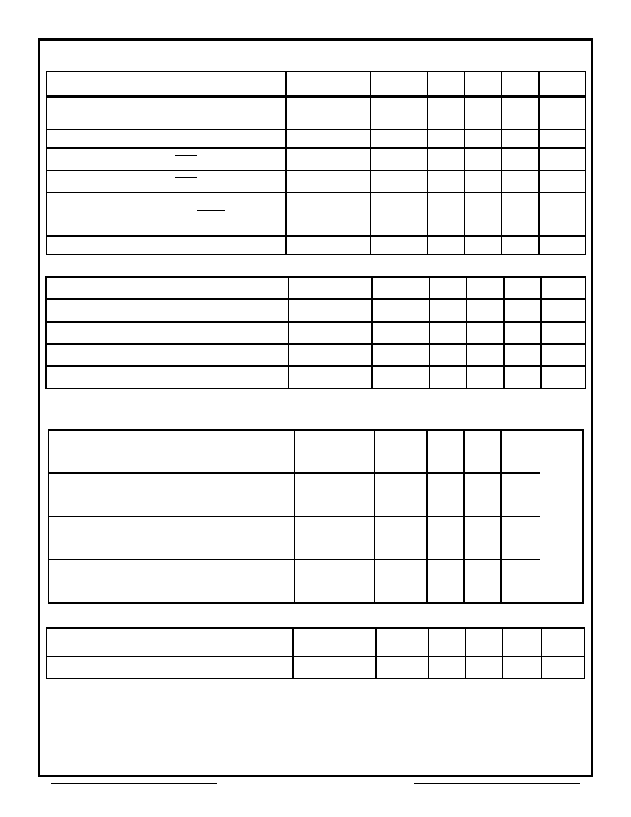
Absolute Maximum Ratings
Operating case temperature
-55∞C to +125∞C
Storage case temperature
-65∞C to +150∞C
Power supply voltage
V
CC
V
EE
V
L
-0.3 V to +18 V
+0.3 V to-18 V
-0.3 V to +7.0 V
Logic input voltage
-0.3 V to +5.5 V
Receiver differential input
±40 V
P
-
P
Receiver input voltage (common mode)
±10 V
Driver peak output current
300 mA
Total package power dissipation over the full operating
case temperature rise
2.5 Watts
(Note: Normal operation conditions require one
transceiver on and the other off)
Maximum junction to case temperature
10∞C
Thermal resistance ≠ junction to case
4∞C/W
Electrical Characteristics -- Driver Section
Input Characteristics, TX DATA IN or TX DATA IN (Notes 2 & 3 apply)
Parameter
Condition
Symbol
Min
Typ
Max
Unit
"0" Input Current
V
IN
= 0.4 V
I
ILD
-0.1
-0.2
mA
"1" Input Current
V
IN
= 2.7 V
I
IHD
1
40
µA
"0" Input Voltage
V
IHD
0.7
V
"1" Input Voltage
V
IHD
2.0
V
Inhibit Characteristics
"0" Input Current
V
IN
= 0.4 V
I
ILI
-0.1
-0.2
mA
"1" Input Current
V
IN
=2.7V
I
IHI
1.0
40
µA
"0" Input Voltage
V
ILI
0.7
V
"1" Input Voltage
V
IHI
2.0
V
Delay from TX inhibit, (0
°
1) to inhibited output
From mid pt
inhibit to
±1.2V pt B,
See Figure 5
t
DXOFF
175
225
nS
Delay from TX inhibit, (1
°
0) to active output
t
DXON
90
150
nS
Differential output noise, inhibit mode
V
NOI
2
10
mV
P-P
Differential output impedance (inhibited) Note 1 See
Figure 5
Point B
Z
OI
2K
Point C
Z
OI
1K
Output Characteristics
Differential output level, See Figure 5
See Figure 5
Point A
V
O
6
7.5
9
V
P-P
Rise and fall times(10% to 90% at pt A output)
See Figure 5
Point A
t
r
100
160
300
nS
Output offset, Figure 3, 2.5µS after midpoint
crossing of the parity bit of the last word of a 660µS
message See Figure 5
Point A
V
OS
± 90
mV peak
Delay from 50% point of TX DATA or TX DATA input
to zero crossing of differential signal. See Fig 5
Point A
t
DXT
100
200
nS
Aeroflex Circuit Technology
SCD4487D REV B 3/10/98 Plainview NY (516) 694-6700
4
Electrical Characteristics -- Receiver Section
Parameter
Condition
Symbol
Min
Typ
Max
Unit
Differential Receiver Input Voltage Range
(See Figure 5, Point B)
TXFMR
1.4:1
V
IDR
40
V
P-P
Common Mode Rejection Ratio (Note 3)
CMRR
45
dB
"1" State ≠ Rx Data or Rx Data Output
I
OH
= -0.4 mA
V
OH
2.5
3.7
V
"0" State ≠ Rx Data or Rx Data Output
I
OI
= 4 mA
V
OL
0.35
0.5
V
Delay (average) from Differential Input Zero
Crossings to RX DATA and RX DATA Output
50% points
t
DXT
270
400
nS
Input Threshold Voltage (referred to the bus)
100KHz≠1MHz
V
TH
0.60
0.75
1.20
V
P-P
Strobe Characteristics (Logic "0" Inhibits Output)
"0" Input Current
V
S
=0.4V
I
IL
-0.1
-0.2
mA
"1" Input Current
V
S
=2.7V
I
IH
1
+40
µA
"0" Input Voltage
V
IL
0.7
V
"1" Input Voltage
V
IH
2.0
V
Strobe Delay (Turn-on or Turn-off)
t
SD
50
100
nS
Power Data
Power Supply Currents ≠ Per Channel ≠ See Figure 4
Transmitter Standby
I
CC
I
EE
I
L
0
12
18
1
16
30
mA
25% duty cycle
I
CC
I
EE
I
L
45
12
18
50
20
30
50% duty cycle
I
CC
I
EE
I
L
90
12
18
100
20
30
100% duty cycle
I
CC
I
EE
I
L
180
12
18
200
20
30
Power Supply Voltages
±15V Operating Power Supply Voltage Range
V
CC
V
EE
+14.25
-14.25
+15.00
-15.00
+15.75
-15.75
V
+5V Operating Power Supply Voltage Range)
V
L
+4.50
+5.00
+5.50
V
Note 1. Power on or off, measured from 75KHz to 1MHz at point A and transformer self impedance of 3K
minimum
at 1MHz.
Note 2: Power Supplies: ±15 Volts ±0.75 V & +5 Volts ±0.5 V, bypassed by 10 µF (Tantalum recommended)
Capacitor minimum. All measurements & specifications apply over the temperature range of -55∞C to +125∞C
(case temperature) unless otherwise specified.
Note 3: When measured as shown per Figure 5 with ± 10 Volt peak, line to ground, DC to 2MHz
Note 4: Typical power is measured with V
BUS
at point A = 7.5 V
P-P
Aeroflex Circuit Technology
SCD4487D REV B 3/10/98 Plainview NY (516) 694-6700
5
Configurations and Ordering Information
ACT
Model # / Ordering Part #
Case
Style
DESC
Number
Rx Standby
ACT 4487-D
DIP
5962-8757910X_
Normally Low
ACT 4487-DI
DIP
5962-TBA
Normally High
ACT 4487-DF
FP
5962-8757910Y_
Normally Low
ACT 4487-DFI
FP
5962-TBA
Normally High
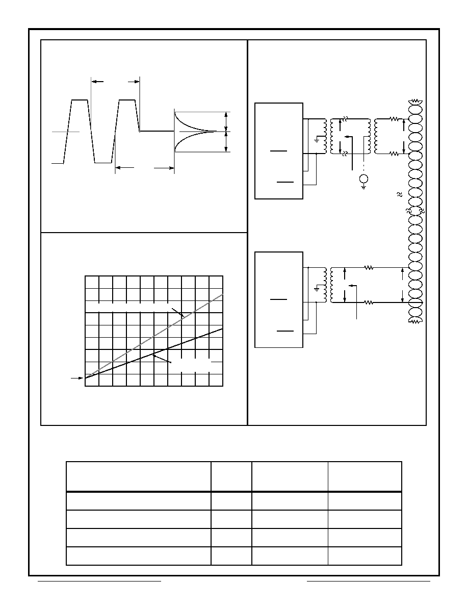
Figure 3 ≠ Transmitter (TX) Output Offset
Figure 4 ≠ Hybrid Power Dissipation vs. Duty Cycle
0 10 20 30 40 50 60 70 80 90 100
3200
2800
2400
2000
1600
1200
800
400
0
DUTY CYCLE ≠ PERCENT
P
O
W
E
R
D
I
S
S
I
P
A
T
I
O
N
M
I
L
L
I
W
A
T
T
S
OUTPUT OFFSET
*
OUTPUT OFFSET
*
LAST BIT
2.5 µsec
*
Offset measured at point A in Figure 5
0 Volts
Magnified View
(Total hybrid with one channel transmitting
and the other not powered ≠ 100% Duty Cycle)
Note: Vcc= +15V, V
EE
= -15V, V
L
= +5V, Transformer ratio 1.4:1,
V
BUS
(point A) at 7.5VP-P.
Figure 5 ≠ Typical 1553 Bus Connections
1.4:1
TX DATA OUT
TX DATA OUT
RX DATA IN
RX DATA IN
70
70
52.5
Transformer Model use Technitrol Part# 1553-2
3
2
1
52.5
8
4
2:1
TX DATA OUT
TX DATA OUT
RX DATA IN
RX DATA IN
52.5
3
2
1
52.5
7
5
1:1.4
Transformer Coupled Stub
Direct Coupled Stub
C
B
Zoi
V
CM
Zoi
A
A
T1553-2
T1553-2
ACT 4487
ACT 4487
0.270
or equivalent
3600
2.97W
1.87W
Typical Hybrid
Dissipation
Typical Hybrid Input Power
Specifications subject to change without notice.