eroflex Circuit T
echnology
≠ Data Bus Modules For The Future © SCD4808 REV E 12/9/99
CIRCUIT TECHNOLOGY
www.aeroflex.com/act1.htm
Features
∑ ACT4808 Dual Transceiver meets
MIL-STD-1553A & B, Macair A3818, A5690, A5232
and A4905 specs
∑ New Low Power Model ≠L Available
∑ Operates with ±12V to ±15V & +5V Power Supplies
∑ Voltage source output for higher bus drive power
∑ Plug-in or Flat Package
∑ Monolithic construction using linear ASICs
∑ Processed and Screened to MIL-STD-883 specs
General Description:
The Aeroflex Laboratories transceiver
model ACT4808 is a new generation
Dual monolithic transceiver which
provides full compliance with Macair
and MIL-STD-1553 data bus
requirements
The model ACT4808 performs the
front-end analog function of inputting
and outputting data through a
transformer to a MIL-STD-1553 or
Macair data bus. The ACT4808 can
be considered a "Universal"
Transceiver in that it is compatible
with MIL-STD-1553A & B, Macair
A-3818, A-4905, A-5232 and A-5690.
Design of this transceiver reflects
particular attention to active filter
performance. This results in low bit
and word error rate with superior
waveform purity and minimal zero
crossover distortion. The ACT4808
series active filter design has
additional high frequency roll-off to
provide the required Macair low
harmonic distortion waveform without
increasing the pulse delay
characteristics significantly.
Efficient transmitter electrical and
thermal design provides low internal
power dissipation and heat rise at
high and well as low duty cycles.The
receiver input threshold is set
Internally.
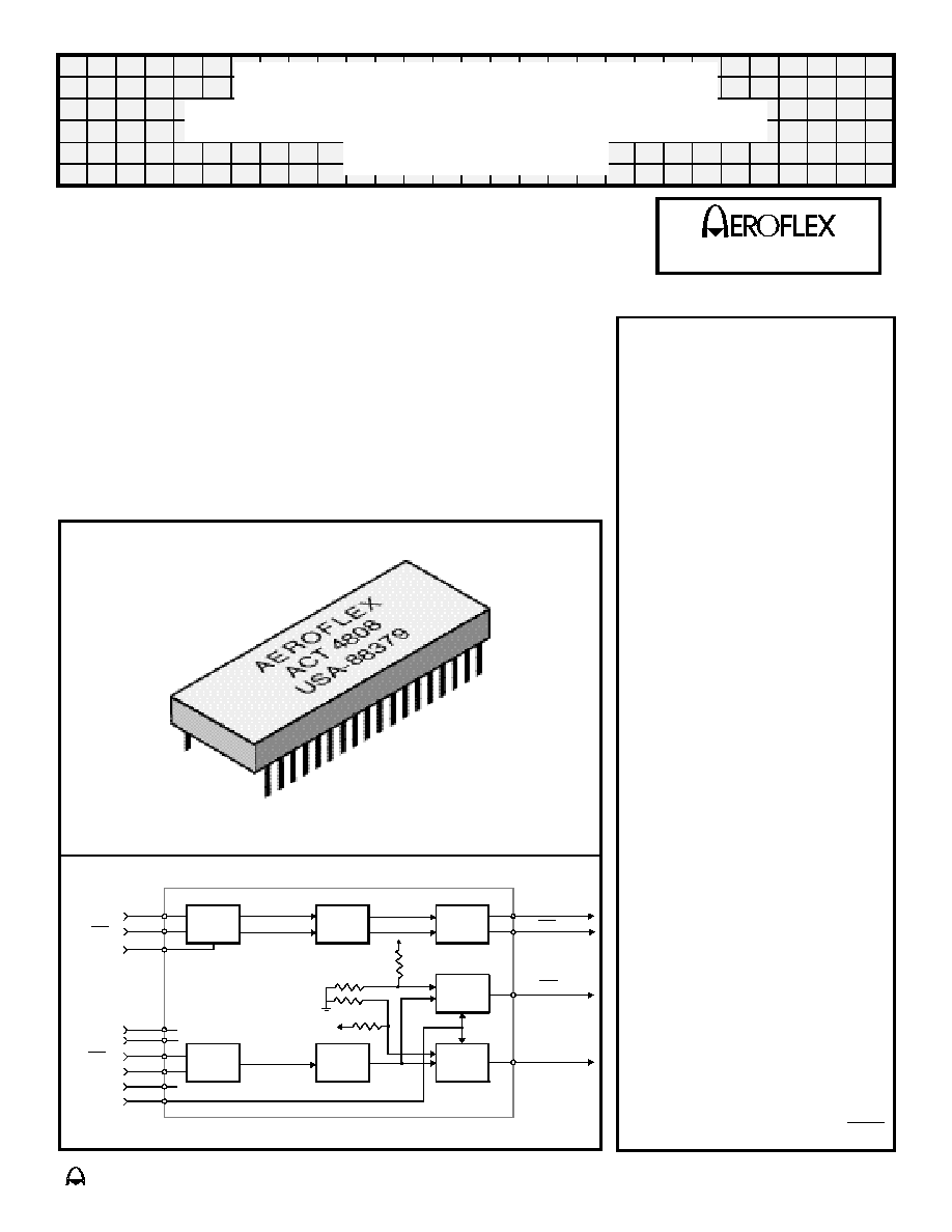
Transmitter
The Transmitter section accepts
bi-phase TTL data at the input and
when coupled to the data bus as per
Figure 3 or 4 and by two 70 Ohm
terminations (Z
O
), the data bus signal
produced is 6.5 Volts minimum P-P at
A-A'. When both DATA and DATA
ACT4808 Transceiver
Block Diagram (without Transformer), 1/2 of unit shown
SHAPING
OUTPUT
STAGE
COMP.
COMP.
ACTIVE
FILTER
INPUT
AMP
DRIVER
TX DATA IN
TX DATA IN
TX INHIBIT
+5 V
RX DATA IN
RX DATA IN
STROBE
TX DATA OUT
TX DATA OUT
RX DATA OUT
RX DATA OUT
V
EE
V
CC
V+
V-
ACT4808 Dual Transceivers for
MACAIR A3818, A5690, A5232, A4905
& MIL-STD-1553
Aeroflex Circuit Technology
SCD4808 REV E 12/9/99 Plainview NY (516) 694-6700
2
inputs are held low or high, the
transmitter output becomes a high
impedance and is "removed" from
the line. In addition, an overriding
"INHIBIT" input provides for the
removal of the transmitter output
from the line. A logic "1" applied to
the "INHIBIT" takes priority over the
condition of the data inputs and
disables the transmitter. (See
Transmitter Logic Waveforms,
Figure 1.)
The transmitter utilizes an active
filter to suppress harmonics above
1 MHz to meet Macair specifications
A-3818, A-4905, A-5232 and
A-5690. The transmitter may be
safely operated for an indefinite
period at 100% duty cycle into a
data bus short circuit (Pt. A-A').
Receiver
The Receiver section accepts
bi-phase differential data at the input
and produces two TTL signals at the
output. The outputs are DATA and
DATA, and represent positive and
negative excursions of the input
beyond a pre-determined threshold.
(See Receiver Logic Waveforms,
Figure 2.)
The internal threshold is nominally
set to detect data bus signals
exceeding 1.10 Volts P-P and reject
signals less than 0.6 Volts P-P
when used with a 1:1 turns ratio
transformer. (See Figure 4 for
transformer data and typical
connection.)
A low level at the Strobe input
inhibits the DATA and DATA
outputs.
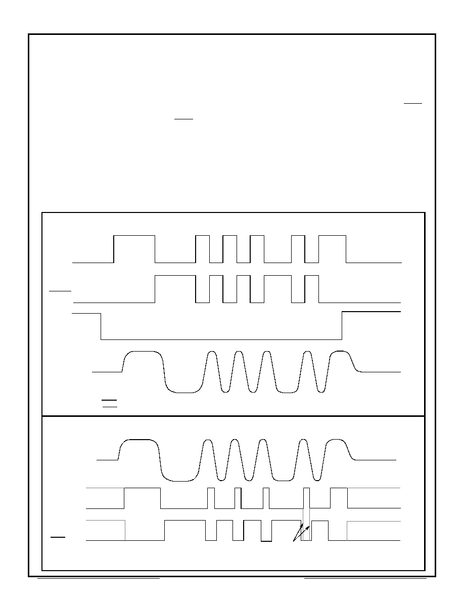
DATA IN
DATA IN
INHIBIT
LINE TO LINE
OUTPUT
NOTES:
2. DATA and DATA inputs must be complementary waveforms or 50% duty cycle average, with no delays between them.
3. DATA and DATA must be in the same state during off time (both high or low).
Figure 1 ≠ Transmitter Logic Waveforms
Figure 2 ≠ Receiver Logic Waveforms
Note overlap
NOTE
:
Waveforms shown are for normally low devices. For normally high receiver output
devices, the receiver outputs are swapped as shown by the dashed lines
level
LINE TO LINE
INPUT
DATA OUT
DATA OUT
1. Line to line waveforms illustrate Macair signals, MIL-STD-1553 signals are trapezoidal

Aeroflex Circuit Technology
SCD4808 REV E 12/9/99 Plainview NY (516) 694-6700
3
Absolute Maximum Ratings, Per Channel
Operating Case Temperature
-55∞C to +125∞C
Storage Case Temperature
-65∞C to +150∞C
Power Supply Voltages
±16 V
+7 V
Logic Input Voltage
-0.3 V to +5.5 V
Receiver Differential Input
±40 V
Receiver Input Voltage (Common Mode)
±10V
Driver Peak Output Current
150 mA
Total Package Power Dissipation over the Full Operating
Case Temperature Range
3.6 Watts
Maximum Junction to Case Temperature
18∞C
Junction-Case, Thermal Resistance
5∞C/W
Electrical Characteristics Per Channel, Transmitter Section
1/ 2/
Input Characteristics, TX DATA IN or TX DATA IN
Parameter
Condition
Symbol
Min
Typ
Max
Unit
"0" Input Current
V
IN
= 0.4 V
I
ILD
-
-0.2
-0.4
mA
"1" Input Current
V
IN
= 2.7 V
I
IHD
-
1.0
40
µA
"0" Input Voltage
-
V
IHD
-
-
0.7
V
"1" Input Voltage
-
V
IHD
2.0
-
-
V
Inhibit Characteristics
"0" Input Current
V
IN
= 0.4 V
I
ILI
-
-0.2
-0.4
mA
"1" Input Current
V
IN
= 2.7 V
I
IHI
-
1.0
40
µA
"0" Input Voltage
-
V
ILI
-
-
0.7
V
"1" Input Voltage
-
V
IHI
2
-
-
V
Delay from TX inhibit(0°1) to inhibited output
-
t
DXOFF
-
300
450
nS
Delay from TX inhibit, (1°0) to active output
-
t
DXON
-
300
450
nS
Differential output noise, inhibit mode
3/
V
NOI
-
0.8
10
mVp-p
Differential output impedance
*
4/
Z
OI
2K
-
-
*
See Aeroflex Application note# 113 for reference.
Output Characteristics
Differential output - Direct coupled stub
Differential output - Transformer coupled stub
(see Fig. 3 and 4)
Pt. B - B'
Z
O
= 70
5/
V
O
26
18
29
21
32
25
Vp-p
Vp-p
Differential output offset - Direct coupled stub Fig. 4
Differential output offset - Xformer coupled stub Fig. 3
V
OS
-
-
-
-
±360
±250
mVpk
mVpk
Differential output rise / fall times (see Fig. 5)
10% - 90%
t
R
& t
F
200
250
300
nS
Delay from 50% point of TX DATA or TX DATA input to
zero crossing of differential output.
-
t
DTX
240
300
nS

Aeroflex Circuit Technology
SCD4808 REV E 12/9/99 Plainview NY (516) 694-6700
4
Electrical Characteristics Per Channel, Receiver Section
1/ 2/
Parameter
Condition
Symbol
Min
Typ
Max
Unit
Differential Input Impedance
f = 1MHz
Z
IN
10K
-
-
Differential Input Voltage Range
-
V
IDR
-
-
40
Vp-p
Input Common Mode Voltage Range
-
V
ICR
10
-
-
Vp-p
Common Mode Rejection Ratio
-
CMRR
40
-
-
dB
Strobe Characteristics (Logic "0" Inhibits Output)
"0" Input Current
V
S
= 0.4 V
I
IL
-
-0.2
-0.4
mA
"1" Input Current
V
S
= 2.7 V
I
IH
-
1.0
+40
µA
"0" Input Voltage
-
V
IL
-
-
0.7
V
"1" Input Voltage
-
V
IH
2.0
-
-
V
Strobe Delay (Turn-on or Turn-off)
-
t
SD
-
-
150
nS
Threshold Characteristics (Sinewave Input )
Internal Threshold Voltage Fig. 4
Pt. B - B'
1MHz
V
TH
0.60
0.80
1.10
Vp-p
Output Characteristics, RX DATA and RX DATA
"1" State
I
OH
= -0.4 mA
V
OH
2.5
3.6
-
V
"0" State
I
OL
= 4 mA
V
OL
-
0.35
0.5
V
Receiver Output Skew
6/
t
RXSK
-
-
10
nS
Delay (average), from differential input zero
crossings to RX DATA and RX DATA output
50% points
7/
t
DRX
-
300
450
nS
Power Supply Currents Per Channel
1/ 2/
V
CC
= +12V to +15V, V
EE
= -12V to -15V, V
L
= +5V
Duty Cycle
Condition
Symbol
Std Version
-L Version
Unit
Typ
Max
Typ
Max
Transmitter
Standby
Pt. B - B'
Z
O
= 70
,
V
O
= 29 V
PK
-
PK
Bit Pattern = FFFF
HEX
Fig. 4
I
CC
I
EE
I
L
30
50
25
60
75
35
5
25
18
10
35
30
mA
25%
I
CC
I
EE
I
L
50
70
25
85
105
35
20
40
18
30
60
30
50%
I
CC
I
EE
I
L
75
45
25
110
130
35
40
60
18
60
80
30
100%
I
CC
I
EE
I
L
120
140
25
160
180
35
85
105
18
120
140
30

Aeroflex Circuit Technology
SCD4808 REV E 12/9/99 Plainview NY (516) 694-6700
5
Notes:
1. V
CC
= +15Volts ±0.75V, V
EE
= -15Volts ±0.75V, V
IL
= +5Volts ±0.5V, T
C
= -55∞C to +125∞C, unless otherwise
specified.
2. All typical values are measured at +25∞C.
3. Characteristics guaranteed by design, not production tested.
4. Power ON/OFF, measured from 75KHz to 1MHz at Point A-A' Figure 4, in accordance with MIL-STD-1553B
paragraph 4.5.2.2.2.3.
5. At point A-A' on Figure 3 or 4, 2.5 µS after midpoint crossing of the parity bit of the last word of a 660 µS message.
6. Receiver skew is defined as the time from the rising edge of RX DATA OUT to the rising edge of RX DATA OUT
minus 500 nS, with a sine wave input of 3 V
PK
-
PK
at 1MHz driven into Pt. B-B' of Figure 4 or 2.1 V
PK
-
PK
at 1MHz
driven into Pt. B-B' of Figure 3. The specification maximum is guaranteed for T
A
= 25∞C only. Standard TTL loads
applied to RX DATA Outputs.
7. This test is peformed while the Transceiver is reading its own transmission. This condition is called "Wraparound".
Standard TTL loads applied to RX DATA Outputs.
Typical Hybrid Power Dissipation
*
, Per Channel
Power
Supply
Conditions
Condition
Std Version
-L Version
Unit
Standby
100%
Duty
Cycle
Standby
100%
Duty
Cycle
PSC1
V
CC
= +15V
V
EE
= -15V
V
L
= +5V
Pt. B - B'
Z
O
= 70
,
V
O
= 29 V
PK
-
PK
Bit Pattern = FFFF
HEX
Fig. 4
1.325
3.250
0.540
2.167
Watts
PSC2
V
CC
= +15V
V
EE
= -12V
V
L
= +5V
1.118
3.142
0.465
1.852
PSC3
V
CC
= +12V
V
EE
= -12V
V
L
= +5V
1.085
2.472
0.450
1.600
*
See Aeroflex Application note# 112 for reference.
Recommended Power Supply Voltage Range
+V
+11.4 Volts to +15.75 Volts
-V
-11.4 Volts to -15.75 Volts
Logic
+4.5 Volts to +5.5 Volts