
CIRCUIT TECHNOLOGY
www.aeroflex.com
eroflex Circuit Technology - Advanced Multichip Modules © SCD3764 REV A 6/2/98
General Description
The ACT-PS512K8 is a
Plastic High Speed, 4 Megabit
(4,194,304 bits) CMOS
Monolithic SRAM organized as
524,288 words by 8 bits.
Designed for high-speed, high
density, high reliablility, mass
memory and fast cache system
applications.
The plastic monolithic is
input and output TTL
compatible. Writing is executed
when the write enable (WE)
and chip enable (CE) inputs are
low. Reading is accomplished
when WE is high and CE and
output enable (OE) are both
low. Access time grades of
10ns 12ns, 15ns, 17ns, 20ns
and 25ns are standard.
512Kx8
OE
A
0
≠
A
18
I/O
0-7
8
WE
CE
Pin Description
I/O
0-7
Data I/O
A
0≠18
Address Inputs
WE
Write Enable
CE
Chip Enable
OE
Output Enable
V
CC
Power Supply
V
SS
Ground
NC
Not Connected
V
ss
V
cc
Block Diagram ≠ SOJ (L2)
Plastic PathTM Features
s
Low Power Monolithic CMOS 512K x 8 SRAM
s
Operating Temperature Range
q
Full Military (-55∞C to +125∞C)
q
Industrial (-40∞C to +85∞C)
s
Burn-in and Temperature Cycle Available
s
10, 12, 15, 17, 20 & 25ns Access Times
s
+5V Power Supply
s
Industry Standard Pinouts
q
Center Power / Ground Pins
s
TTL Compatible I/O
s
3.3V Device I/O Interfacing
s
JEDEC Standard 36 pin Plastic SOJ Package
q
36 Lead, .93" x .405" x 0.148 Small Outline J lead (SOJ),
Aeroflex code# "L2"
s
Fully Static Operation
q
No Clocks or Refresh Required
4 Megabit Plastic Monolithic SRAM
ACT-PS512K8 High Speed
F
I
E
I
D
C
E
R T
A
E
R
O
F
L E
X L A
B
S
I
N
C
.
ISO
9001

Aeroflex Circuit Technology
SCD3764 REV A 6/2/98 Plainview NY (516) 694-6700
2
Absolute Maximum Ratings
Symbol
Parameter
MINIMUM
MAXIMUM
Units
T
C
Case Operating Temperature
-55
+125
∞C
T
STG
Storage Temperature
-65
+150
∞C
P
D
Maximum Package Power Dissipation
1.0
W
V
G
Maximum Signal Voltage to Ground
-0.5
V
CC
+ 0.5
V
V
CC
Power Supply Voltage
-0.5
+7.0
V
Recommended Operating Conditions
Symbol
Parameter
Minimum
Maximum
Units
V
CC
Power Supply Voltage
+4.5
+5.5
V
V
SS
Ground
0
0
V
V
IH
Input High Voltage
+2.2
V
CC
+ 0.5
V
V
IL
Input Low Voltage
-0.5
+0.8
V
T
C
Operating Temperature (Military)
-55
+125
∞C
T
C
Operating Temperature (Industrial)
-40
+85
∞C
Truth Table
Mode
CE
WE
OE
Data I/O
Supply
Current
Standby
H
X
X
High Z
I
SB
Output Disable
L
H
H
High Z
I
CC
Read
L
H
L
Data OUT
I
CC
Write
L
L
X
Data IN
I
CC
Capacitance
(V
IN
& V
OUT
= 0V, f = 1MHz, T
C
= 25∞C, unless otherwise noted, Guaranteed but not tested
)
Symbol
Parameter
Maximum
Units
C
IN
Input Capacitance (A
0-18
, WE & OE)
6
pF
C
OUT
Output Capacitance (I/O
0-7
& CE)
8
pF
DC Characteristics
(V
CC
= 5.0V, V
SS
= 0V, T
C
= -55∞C to +125∞C or -40∞C to +85∞C)
Parameter
Sym
Conditions
Min
Max
Units
Input Leakage Current
I
LI
V
CC
= Max, V
IN
= V
SS
to V
CC
-10
+10
µA
Output Leakage Current
I
LO
CE = V
IH
, OE = V
IH
, V
OUT
= V
SS
to V
CC
-10
+10
µA
Operating Supply Current
I
CC
CE = V
IL
, OE = V
IH
,f =5MHz,Vcc=5.5V
130
mA
Standby Current
I
SB
CE = V
IH
, OE= V
IH
, f =5MHz,Vcc=5.5V
20
mA
Output Low Voltage
V
OL
I
OL
= 8 mA, Vcc = 4.5V
0.4
V
Output High Voltage
V
OH
I
OH
= -4 mA, Vcc = 4.5V
2.4
V
Note: DC Test conditions: V
IL
= 0.3V, V
IH
= Vcc - 0.3V.
Aeroflex Circuit Technology
SCD3764 REV A 6/2/98 Plainview NY (516) 694-6700
3
AC Characteristics
(V
CC
= 5.0V, V
SS
= 0V, T
C
= -55∞C to +125∞C or -40∞C to +85∞C)
Read Cycle
Parameter
Sym
≠010
Min Max
≠012
Min Max
≠015
Min Max
≠017
Min Max
≠020
Min Max
≠025
Min Max
Units
Read Cycle Time
t
RC
10
12
15
17
20
25
ns
Address Access Time
t
AA
10
12
15
17
20
25
ns
Chip Enable Access Time
t
ACE
10
12
15
17
20
25
ns
Output Hold from Address Change
t
OH
3
3
3
3
4
5
ns
Output Enable to Output Valid
t
OE
5
6
7
8
10
12
ns
Chip Enable to Output in Low Z (1)
t
CLZ
3
3
3
3
3
3
ns
Output Enable to Output in Low Z (1)
t
OLZ
0
0
0
0
0
0
ns
Chip Deselect to Output in High Z (1)
t
CHZ
5
6
7
7
8
10
ns
Output Disable to Output in High Z (1)
t
OHZ
5
6
7
7
8
10
ns
Note 1. Guaranteed by design, but not tested
Write Cycle
Parameter
Sym
≠010
Min Max
≠012
Min Max
≠015
Min Max
≠017
Min Max
≠020
Min Max
≠025
Min Max
Units
Write Cycle Time
t
WC
10
12
15
17
20
25
ns
Chip Enable to End of Write
t
CW
7
8
10
12
13
15
ns
Address Valid to End of Write
t
AW
7
8
10
12
13
15
ns
Data Valid to End of Write
t
DW
5
6
8
8
9
10
ns
Write Pulse Width
t
WP
7
8
10
12
13
15
ns
Address Setup Time
t
AS
0
0
0
0
0
0
ns
Address Hold Time
t
AH
0
0
0
0
0
0
ns
Output Active from End of Write (1)
t
OW
3
3
3
3
4
5
ns
Write to Output in High Z (1)
t
WHZ
5
6
7
8
8
10
ns
Data Hold from Write Time
t
DH
0
0
0
0
0
0
ns
Note 1. Guaranteed by design, but not tested
Data Retention Electrical Characteristics (Special Order Only)
V
CC
= 5.0V, V
SS
= 0V, T
C
= -55∞C to +125∞C or -40∞C to +85∞C)
Parameter
Sym
Test Conditions
All Speeds
Min Typ Max
Units
V
CC
for Data Retention
V
DR
CE
V
CC
≠ 0.2V
2
5.5
V
Data Retention Current
I
CCDR1
V
CC
= 3V
0.5
2.0
mA

Aeroflex Circuit Technology
SCD3764 REV A 6/2/98 Plainview NY (516) 694-6700
4
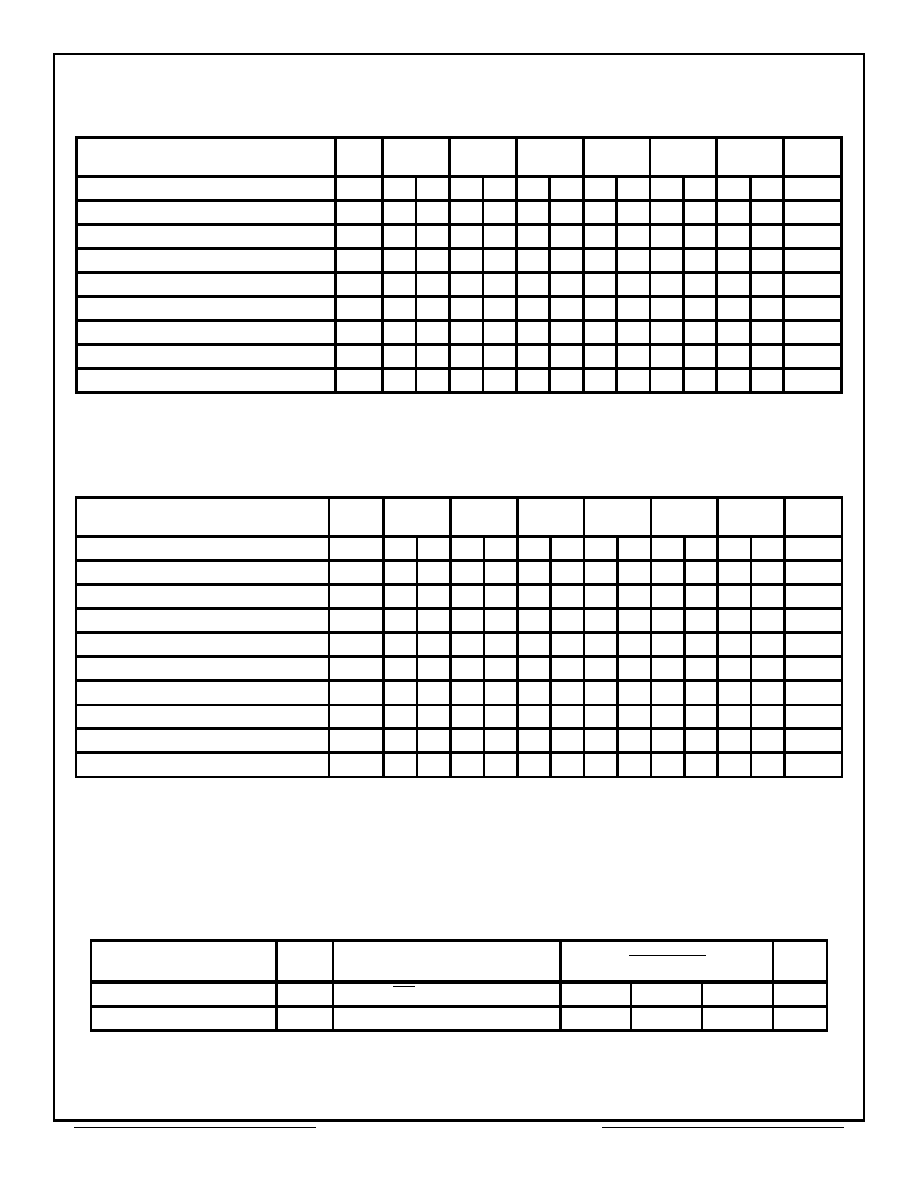
Timing Diagrams -- SRAM
D
I/O
t
RC
t
OH
t
AA
Data Valid
Previous Data Valid
t
OE
High Z
t
OHZ
Read Cycle Timing Diagrams
Data Valid
t
CLZ
SCE
OE
t
ACE
t
CHZ
UNDEFINED
DON'T CARE
Read Cycle 2 (SWE = V
IH
)
Write Cycle (SCE Controlled, OE = V
IH
)
t
CW
t
AS
t
WP
t
DW
t
OW
SCE
SWE
Data Valid
Write Cycle (SWE Controlled, OE = V
IH
)
D
I/O
AC Test Circuit
I
OL
Parameter
Typical
Units
Input Pulse Level
0 ≠ 3.0
V
Input Rise and Fall
5
ns
Input and Output Timing Reference Level
1.5
V
Notes:
1) V
Z
is programmable from -2V to +7V. 2) I
OL
and I
OH
programmable from 0 to 16 mA. 3) Tester Impedance
Z
O
= 75
. 4)
V
Z
is typically the midpoint of V
OH
and V
OL
. 5) I
OL
and I
OH
are adjusted to simulate a typical resistance
load circuit. 6) ATE Tester includes jig capacitance.
I
OH
To Device Under Test
V
Z
~ 1.5 V (Bipolar Supply)
Current Source
Current Source
C
L
= 50 pF
t
WC
t
AW
t
AH
t
RC
t
AA
t
OLZ
S
EE
N
OTE
S
EE
N
OTE
S
EE
N
OTE
S
EE
N
OTE
Note: Guaranteed by design, but not tested.
D
I/O
t
DH
t
WHZ
S
EE
N
OTE
Read Cycle 1 (SCE = OE = V
IL
, SWE = V
IH
)
Write Cycle Timing Diagrams
t
WP
t
DW
Data Valid
t
WC
t
AW
t
AH
D
I/O
t
DH
SCE
SWE
t
CW
t
AS
A
0-18
A
0-18
A
0-18
A
0-18
AC Test Conditions

Aeroflex Circuit Technology
SCD3764 REV A 6/2/98 Plainview NY (516) 694-6700
5
Pin Numbers & Functions
36 Pins -- SOJ
Pin #
Function
Pin #
Function
1
A
0
19
NC
2
A
1
20
A
10
3
A
2
21
A
11
4
A
3
22
A
12
5
A
4
23
A
13
6
CE
24
A
14
7
I/O
0
25
I/O
4
8
I/O
1
26
I/O
5
9
V
CC
27
V
CC
10
V
SS
28
V
SS
11
I/O
2
29
I/O
6
12
I/O
3
30
I/O
7
13
WE
31
OE
14
A
5
32
A
15
15
A
6
33
A
16
16
A
7
34
A
17
17
A
8
35
A
18
18
A
9
36
NC
All dimensions in inches
Dimensions in inches (.xxx)
Package Outline "L2" -- SOJ Package, 36 Leads
11.30 (.445)
11.05 (.435)
9.65 (.380)
9.14 (.360)
.69
(.027)
23.62 (.930)
23.37 (.920)
10.29 (.405)
10.03 (.395)
0.95
(.037)
1.27
(.050)
.43
(.017
3.76 (.148) MAX
Dimensions in millmeters mm
1
18
19
36
MIN
TYP
+.10
-.05
+.004)
-.002)
TYP
.004 MAX