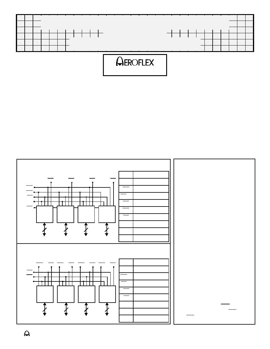
eroflex Circuit Technology - Advanced Multichip Modules © SCD1661B REV A 1/16/97
General Description
Utilizing Intel's SmartVoltage
Boot Block Flash Memory
SmartDieTM, the ACT≠F1M32 is
a high speed, 32 megabit CMOS
flash multichip module (MCM)
designed for full temperature
range military, space, or high
reliability applications.
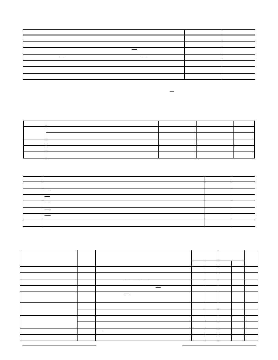
The ACT-F1M32 consists of
four high-performance Intel
X28F800BV 8 Mbit (8,388,608
bit) memory die. Each die
contains separately erasable
blocks, including a hardware
lockable boot block (16,384
bytes), two parameter blocks
(8,192 bytes each), and 8 main
blocks (one block of 98,304
bytes and seven blocks of
131,072 bytes) This defines the
boot block flash family
architecture.
The command register is
written by bringing WE to a logic
low level (V
IL
), while CE is low
and OE is high (V
IH
)
. Reading is
Features
Block Diagram ≠ CQFP(F14)
Block Diagram ≠ CQFP(F14)
s
4 Low Voltage/Power Intel 1M x 8 FLASH Die in One
MCM Package
s
Overall Configuration is 1M x 32
s
+5V Operation (Standard) or +3.3V (Consult Factory)
s
Access Times of 80, 100 and 120 nS ( 5V V
CC
)
s
+5V or +12V Programing
s
Erase/Program Cycles
q
100,000 Commercial
q
10,000 Military and Industrial
s
Sector Architecture (Each Die)
q
One 16K Protected Boot Block (Bottom Boot Block
Standard, Top Boot Block Special Order)
q
Two 8K Parameter Blocks
q
One 96K Main Block
q
Seven 128K Main Blocks
s
Single Block Erase (All bits set to 1)
s
Hardware Data Protection Feature
s
Independent Boot Block Locking
s
MIL-PRF-38534 Compliant MCMs Available
s
Packaging ≠ Hermetic Ceramic
q
68 Lead, .94" x .94" x .180" Dual-Cavity Small
Outline Gull Wing, Aeroflex code# "F14" (Drops into
the 68 Lead JEDEC .99"SQ CQFJ footprint)
s
Internal Decoupling Capacitors for Low Noise
Operation
s
Commercial, Industrial and Military Temperature
Ranges
CIRCUIT TECHNOLOGY
Standard Configuration
Pin Description
I/O
0-31
Data I/O
A
0≠19
Address Inputs
WE
Write Enables
CE
1-4
Chip Enables
OE
Output Enable
WP
Write Protect
RP
Reset/Powerdown
V
CC
Power Supply
GND
Ground
NC
Not Connected
Pin Description
I/O
0-31
Data I/O
A
0≠19
Address Inputs
WE
1-4
Write Enable
CE
1-4
Chip Enables
OE
Output Enable
RP
Reset/Powerdown
V
CC
Power Supply
GND
Ground
NC
Not Connected
1Mx8
1Mx8
1Mx8
1Mx8
CE
4
OE
A
0
≠
A
19
I/O
0-7
I/O
8-15
I/O
16-23
I/O
24-31
8
8
8
8
CE
3
WE
4
WE
3
WE
2
WE
1
CE
1
CE
2
RP
1Mx8
1Mx8
1Mx8
1Mx8
CE
4
OE
A
0
≠
A
19
I/O
0-7
I/O
8-15
I/O
16-23
I/O
24-31
8
8
8
8
CE
3
WE
CE
1
CE
2
WP
RP
Optional Configuration
www.aeroflex.com/act1.htm
Boot Block
FLASH Multichip Module
ACT≠F1M32 High Speed 32 Megabit

Aeroflex Circuit Technology
SCD1661B REV A 1/16/97 Plainview NY (516) 694-6700
2
accomplished by chip Enable (CE) and
Output Enable (OE) being logically active.
Access time grades of 80nS, 100nS and
120nS maximum are standard.
The ACT≠F1M32 is packaged in a
hermetically sealed co-fired ceramic 68
lead, .94" SQ Ceramic Gull Wing CQFP
package. This allows operation in a military
environment temperature range of -55∞C to
+125∞C.
The ACT≠F1M32 provides program and
erase capability at 5V or 12V and allows
reads with Vcc at 5V or 3.3V(Not tested).
Since many designs read from flash
memory a large percentage of the time,
read operation using 3.3V can provide
great power savings. Consult the factory for
3.3V tested parts. In applications where
read performance is critical, faster access
times are obtainable with the 5V V
CC
part
detailed herein.
For program and erase operations, 5V
Vpp operation eliminates the need for in
system voltage converters. The 12V Vpp
operation provides reduced (approx 60%)
program and erase times where 12V is
available in the system. For design
simplicity, however, connect Vcc and Vpp
to the same 5V ±10% source.
Each block can be independently
erased and programmed 100,000 times at
commercial temperature or 10,000 times at
extended temperature.
The boot block is located at either the
bottom (Standard) or the top (Special
Order) of the address map in order to
accommodate different microprocessor
protocols for boot code location. Locking
and unlocking of the boot block is controlled
by WP and/or RP.
Intel's boot block architecture provides a
flexible solution for the different design
needs of various applications. The
asymmetrically-blocked memory map
allows the integration of several memory
components into a single flash device. The
boot block provides a secure boot PROM;
the parameter blocks can emulate
EEPROM functionality for parameter store
with proper software techniques; and the
main blocks provide code and data storage
with access times fast enough to execute
code in place, decreasing RAM
requirements.
For Detail Information regarding the
operation of the 28F800BV Memory die,
see the Intel datasheet (order number
290539-002).
General Description, Cont'd
,
SmartDieTM is a Trademark of Intel Corporation
Aeroflex Circuit Technology
SCD1661B REV A 1/16/97 Plainview NY (516) 694-6700
3
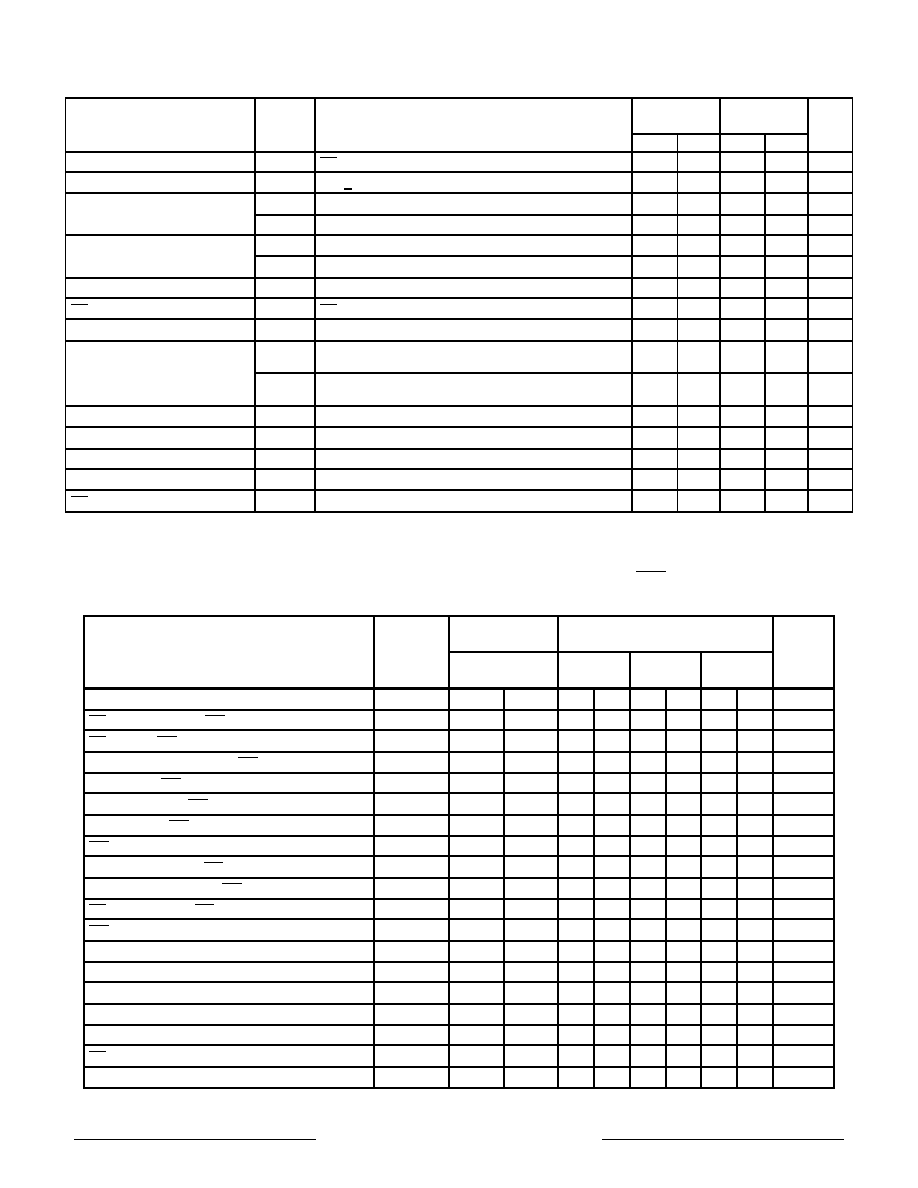
Absolute Maximum Ratings
Parameter
Range
Units
Case Operating Temperature Range
-55 to +125
∞
C
Storage Temperature Range
-65 to +150
∞
C
Voltage on Any Pin with Respect to GND (except V
CC
, V
PP
, A
9
and
RP)
(1)
-2.0 to +7.0
V
Voltage on Pins A
9
or
RP with Respect to GND (except V
CC
, V
PP
, A
9
and
RP)
(1,2)
-2.0 to +13.5
V
V
PP
Program Voltage with Respect to GND during Block Erase/ and Word/Byte Write
(1,2)
-2.0 to +14.0
V
Vcc Supply Voltage with Respect to Ground
(1)
-2.0 to +7.0
V
Output Short Circuit Current
(3)
100
mA
Notes:
1. Minimum DC voltage is -0.5V on input/output pins. During Transitions, inputs may undershoot to -2.0V for periods < 20nS. Maximum DC voltage on input/output
pins is Vcc + 0.5V, which may overshoot to Vcc + 2.0V for periods < 20nS.
2. Maximum DC voltage on Vpp may overshoot to +14.0V for periods < 20nS. Maximum DC voltage on RP or A
9
may overshoot to V
CC
+ 0.5V for periods <20nS
3. Output shorted for no more than 1 second. No more than one output shorted at one time.
NOTICE: Stresses above those listed under "Absolute Maximums Rating" may cause permanent damage. These are stress rating only. Operation beyond the "Oper-
ation Conditions" is not recommended and extended exposure beyond the "Operation Conditions" may effect device reliability.
Recommended Operating Conditions
Symbol
Parameter
Minimum
Maximum
Units
V
CC
5V Power Supply Voltage (10%)
+4.5
+5.5
V
3.3V Power Supply Voltage (±0.3V) (Consult Factory)
+3.0
+3.6
V
V
IH
Input High Voltage (3.3V & 5V V
CC
)
+2.0
V
cc
+ 0.5
V
V
IL
Input Low Voltage (3.3V & 5V V
CC
)
-0.5
+0.8
V
T
A
Operating Temperature (Military)
-55
+125
∞
C
Capacitance
(f = 1MHz, T
A
= 25
∞
C)
Symbol
Parameter
Maximum
Units
C
AD
A0 ≠ A19
Capacitance
50
pF
C
OE
OE Capacitance
50
pF
C
CE
CE Capacitance
20
pF
C
RP
RP Capacitance
50
pF
C
WE
WE Capacitance
60
pF
C
WP
WP Capacitance
50
pF
C
I
/
O
I/O0 ≠ I/O31 Capacitance
20
pF
Capacitance Guaranteed by design, but not tested.
DC Characteristics ≠ CMOS Compatible
(T
A
= -55
∞
C to +125
∞
C, V
CC
= +4.5V to + 5.5V(5V Operation), or +3.0V to +3.6V(3.3V Operation), Unless otherwise specified)
Parameter
Sym
Conditions
+3.3V V
CC
(1)
Typical
+5.0V V
CC
Standard
Units
Min
Max
Min
Max
Input Load Current
I
IL
V
CC
= V
CC
Max., V
IN
= V
CC
or GND
-1
+1
-1
+1
µ
A
Output Leakage Current
I
LO
V
CC
= V
CC
Max., V
IN
= V
CC
or GND
-10
+10
-10
+10
µ
A
Vcc Standby Current
I
CCS
V
CC
= V
CC
Max., CE = RP = WP = V
CC
± 0.2V
440
600
µ
A
Vcc Deep Power-Down Current
I
CCD
V
CC
= V
CC
Max., V
IN
= V
CC
or GND, RP = GND ± 0.2V
32
32
µ
A
Vcc Read Current
I
CCR
V
CC
= V
CC
Max., CE = GND, f = 10MHz (5V), 5MHz (3.3V),
I
OUT
= 0 mA, Inputs = GND ± 0.2V or V
CC
± 0.2V
120
260
mA
Vcc Write Current
I
CCW
1
V
PP
= V
PPH
1
(at 5V), Word Write in Progress (x32)
120
200
mA
I
CCW
2
V
PP
= V
PPH
2
(at 12V), Word Write in Progress (x32)
100
180
mA
Vcc Erase Current
I
CCE
1
V
PP
= V
PPH
1
(at 5V),Block Erase in Progress
120
180
mA
I
CCE
2
V
PP
= V
PPH
2
(at 12V),Block Erase in Progress
100
160
mA
Vcc Erase Suspend Current
I
CCES
CE = V
IH
, Block Erase Suspend
32
48
mA
V
PP
Standby Current
I
PPS
V
PP
< V
PPH
2
60
60
µ
A
Aeroflex Circuit Technology
SCD1661B REV A 1/16/97 Plainview NY (516) 694-6700
4
V
PP
Deep Power Down Current
I
PPD
RP = GND ± 0.2V
40
40
µ
A
V
PP
Read Current
I
PPR
V
PP
> V
PPH
2
800
800
µ
A
V
PP
Write Current
I
PPW
1
V
PP
= V
PPH
1
(at 5V), Word Write in Progress (x32)
120
120
mA
I
PPW
2
V
PP
= V
PPH
2
(at 12V), Word Write in Progress (x32)
100
100
mA
V
PP
Erase Current
I
PPE
1
V
PP
= V
PPH
1
(at 5V), Block Erase in Progress
120
100
mA
I
PPE
2
V
PP
= V
PPH
2
(at 12V), Block Erase in Progress
100
80
mA
V
PP
Erase Suspend Current
I
PPES
V
PP
= V
PPH
,
Block Erase Suspend in Progress
800
800
µ
A
RP Boot Block Unlock Current
I
RP
RP = V
HH
, V
PP
= 12V
2
2
mA
Output Low Voltage
V
OL
V
CC
= V
CC
Min., I
OL
= 5.8 mA (5V), 2 mA (3.3V)
0.45
0.45
V
Output High Voltage
V
OH
1
V
CC
= V
CC
Min., I
OH
= -2.5 mA
0.85 x
V
CC
0.85 x
V
CC
V
V
OH
2
V
CC
= V
CC
Min., I
OH
= -100 µA
V
CC
-
0.4V
V
CC
-
0.4V
V
V
PP
Lock-Out Voltage
V
PPLK
Complete Write Protection
0.0
1.5
0.0
1.5
V
V
PP
(Program/Erase Operations)
V
PPH
1
V
PP
= at 5V
4.5
5.5
4.5
5.5
V
V
PP
(Program/Erase Operations)
V
PPH
2
V
PP
= at 12V
11.4
12.6
11.4
12.6
V
V
CC
Erase/Write Lock Voltage
V
LKO
Locked Condition
0
2.0
0
2.0
V
RP Unlock Voltage
V
HH
Boot Block Write/Erase, V
PP
= 12V
11.4
12.6
11.4
12.6
V
Notes:
1. Performance at V
CC
= +4.5V to +5.5V is guaranteed. Performance at V
CC
= +3.3V is typical (Not tested).
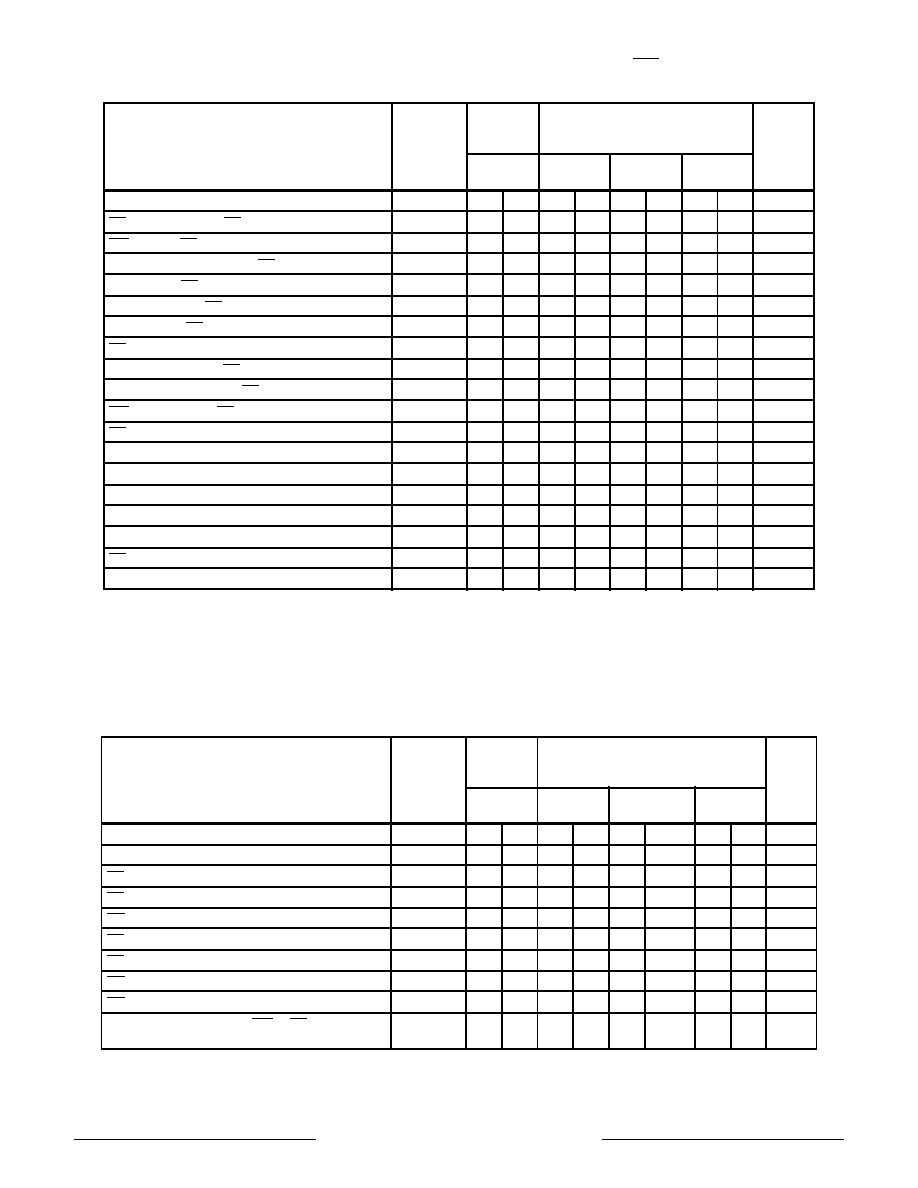
AC Characteristics ≠ Write/Erase/Program Operations ≠ WE Controlled
(T
A
= -55
∞
C to +125
∞
C, V
CC
= +4.5V to + 5.5V(5V Operation), or +3.0V to +3.6V(3.3V Operation), Unless otherwise specified)
Parameter
Symbol
JEDEC
Standard
+3.3V V
CC
(2)
Typical
+4.5V to +5.5V V
CC
Units
120nS
Min Max
80nS
Min Max
100nS
Min Max
120nS
Min Max
Write Cycle Time
t
AVAV
120
80
100
120
nS
RP High Recovery to WE Going Low
t
PHWL
1.5
.45
.45
.45
µ
S
CE Setup to WE Going Low
t
ELWL
0
0
0
0
nS
Boot Block Unlock Setup to WE Going High
(1)
t
PHHWH
200
100
100
100
nS
V
PP
Setup to WE Going High
(1)
t
VPWH
200
100
100
100
nS
Address Setup to WE Going High
t
AVWH
90
60
60
60
nS
Data Setup to WE Going High
t
DVWH
70
60
60
60
nS
WE Pulse Width
t
WLWH
90
60
60
60
nS
Data Hold Time from WE High
t
WHDX
0
0
0
0
nS
Address Hold Time from WE High
t
WHAX
0
0
0
0
nS
CE Hold Time from WE High
t
WHEH
0
0
0
0
nS
WE Pulse Width High
t
WHWL
30
20
20
20
nS
Duration of Word Write Operation
(1)
(x32)
t
WHQV
1
6
6
6
6
µ
S
Duration of Erase Operation (Boot)
(1)
t
WHQV
2
0.3
0.3
0.3
0.3
Sec
Duration of Erase Operation (Parameter)
(1)
t
WHQV
3
0.3
0.3
0.3
0.3
Sec
Duration of Erase Operation (Main)
(1)
t
WHQV
4
0.6
0.6
0.6
0.6
Sec
V
PP
Hold from Valid SRD
(1)
t
QVVL
0
0
0
0
nS
RP V
HH
Hold from Valid SRD
(1)
t
QVPH
0
0
0
0
nS
Boot Block Lock Delay
(1)
t
PHBR
200
100
100
100
nS
Notes:
1. Guaranteed by design, not tested.
2. Performance at V
CC
= +4.5V to +5.5V is guaranteed. Performance at V
CC
= +3.3V is typical (Not tested).
DC Characteristics ≠ CMOS Compatible
(T
A
= -55
∞
C to +125
∞
C, V
CC
= +4.5V to + 5.5V(5V Operation), or +3.0V to +3.6V(3.3V Operation), Unless otherwise specified)
Parameter
Sym
Conditions
+3.3V V
CC
(1)
Typical
+5.0V V
CC
Standard
Units
Min
Max
Min
Max
Aeroflex Circuit Technology
SCD1661B REV A 1/16/97 Plainview NY (516) 694-6700
5
AC Characteristics ≠ Write/Erase/Program Operations, CE Controlled
(T
A
= -55
∞
C to +125
∞
C, V
CC
= +4.5V to + 5.5V(5V Operation), or +3.0V to +3.6V(3.3V Operation), Unless otherwise specified)
Parameter
Symbol
JEDEC
Standard
+3.3V
V
CC
(2)
Typical
+4.5V to +5.5V V
CC
Units
120nS
Min Max
80nS
Min Max
100nS
Min Max
120nS
Min Max
Write Cycle Time
t
AVAV
120
80
100
120
nS
RP High Recovery to CE Low
t
PHEL
1.5
.45
.45
.45
µ
S
WE Setup to CE Going Low
t
WLEL
0
0
0
0
nS
Boot Block Unlock Setup to CE Going High
(1)
t
PHHEH
200
100
100
100
nS
V
PP
Setup to CE Going High
(1)
t
VPEH
200
100
100
100
nS
Address Setup to CE Going High
t
AVEH
90
60
60
60
nS
Data Setup to CE Going High
t
DVEH
70
60
60
60
nS
CE Pulse Width
t
ELEH
90
60
60
60
nS
Data Hold Time from CE High
t
EHDX
0
0
0
0
nS
Address Hold Time from CE High
t
EHAX
0
0
0
0
nS
WE Hold Time from CE High
t
EHWH
0
0
0
0
nS
CE Pulse Width High
t
EHEL
20
20
20
20
nS
Duration of Word Write Operation
(1)
(x32)
t
EHQV
1
6
6
6
6
µ
S
Duration of Erase Operation (Boot)
(1)
t
EHQV
2
0.3
0.3
0.3
0.3
Sec
Duration of Erase Operation (Parameter)
(1)
t
EHQV
3
0.3
0.3
0.3
0.3
Sec
Duration of Erase Operation (Main)
(1)
t
EHQV
4
0.6
0.6
0.6
0.6
Sec
V
PP
Hold from Valid SRD
(1)
t
QVVL
0
0
0
0
nS
RP V
HH
Hold from Valid SRD
(1)
t
QVPH
0
0
0
0
nS
Boot Block Lock Delay
(1)
t
PHBR
200
100
100
100
nS
NOTES:
1. Sampled, but not 100% tested.
2. Performance at V
CC
= +4.5V to +5.5V is guaranteed. Performance at V
CC
= +3.3V is typical (Not Tested).
AC Characteristics ≠ Read Only Operations
(T
A
= -55
∞
C to +125
∞
C, V
CC
= +4.5V to + 5.5V(5V Operation), or +3.0V to +3.6V(3.3V Operation), Unless otherwise specified)
Parameter
Symbol
JEDEC
Standard
+3.3V
V
CC
(2)
Typical
+4.5V to +5.5V V
CC
Units
120nS
Min Max
80nS
Min Max
100nS
Min Max
120nS
Min Max
Read Cycle Time
t
AVAV
120
80
100
120
nS
Address to Output Delay
t
AVQV
120
80
100
120
nS
CE to Output Delay
t
ELQV
120
80
100
120
nS
RP to Output Delay
t
PHQV
1.5
.45
.45
.45
µ
S
OE to Output Delay
t
GLQV
65
40
40
40
nS
CE to Output in Low Z
(1)
t
ELQX
0
0
0
0
nS
CE to Output in High Z
(1)
t
EHQZ
55
30
30
30
nS
OE to Output in Low Z
(1)
t
GLQX
0
0
0
0
nS
OE to Output in High Z
(1)
t
GHQZ
45
30
30
30
nS
Output Hold from Address, CE, or OE Change,
Whichever Occurs First
(1)
t
OH
0
0
0
0
nS
Notes:
1. Guaranteed by design, but not tested.
2. Performance at V
CC
= +4.5V to +5.5V is guaranteed. Performance at V
CC
= +3.3V is typical (Not Tested).