eroflex Circuit Technology - Advanced Multichip Modules © SCD1668 REV A 4/28/98
CIRCUIT TECHNOLOGY
www.aeroflex.com
General Description
The ACT≠F512K8 is a high
speed, 4 megabit CMOS
monolithic Flash module
designed for full temperature
range military, space, or high
reliability applications.
This device is input TTL and
output CMOS compatible. The
command register is written by
bringing WE to a logic low level
(V
IL
), while CE is low and OE is
at logic high level (V
IH
)
. Reading
is accomplished by chip Enable
(CE) and Output Enable (OE)
being logically active, see
Figure 9. Access time grades of
60ns, 70ns, 90ns, 120ns and
150ns maximum are standard.
The ACT≠F512K8 is
available in a choice of
Features
s
Low Power Monolithic 512K x 8 FLASH
s
TTL Compatible Inputs and CMOS Outputs
s
Access Times of 60, 70, 90, 120 and 150ns
s
+5V Programing, 5V
±
10% Supply
s
100,000 Erase / Program Cycles
s
Low Standby Current
s
Page Program Operation and Internal
Program Control Time
s
Supports Full Chip Erase
s
Embedded Erase and Program Algorithms
s
Supports Full Chip Erase
s
MIL-PRF-38534 Compliant Circuits Available
s
Industry Standard Pinouts
s
Packaging ≠ Hermetic Ceramic
q
32 Lead, 1.6" x .6" x .20" Dual-in-line Package (DIP),
Aeroflex code# "P4"
q
32 Lead, .82" x .41" x .11" Ceramic Flat Package
(FP), Aeroflex code# "F6"
q
32 Lead, .82" x .41" x .132" Ceramic Flat Package
(FP Lead Formed), Aeroflex code# "F7"
s
Sector Architecture
q
8 Equal size sectors of 64K bytes each
q
Any Combination of Sectors ccan be erased with one
command sequence.
s
Commercial, Industrial and Military
Temperature Ranges
s
DESC SMD Pending
5962-96692 (P4,F6,F7)
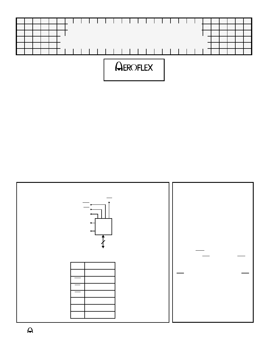
Block Diagram ≠ DIP (P4) & Flat Packages (F6,F7)
512Kx8
OE
A
0
≠
A
18
I/O
0-7
8
WE
CE
Vss
Vcc
Pin Description
I/O
0-7
Data I/O
A
0≠18
Address Inputs
WE
Write Enable
CE
Chip Enable
OE
Output Enable
V
CC
Power Supply
V
SS
Ground
NC
Not Connected
ACT≠F512K8 High Speed
4 Megabit Monolithic FLASH

Aeroflex Circuit Technology
SCD1668 REV A 4/28/98 Plainview NY (516) 694-6700
2
hermetically sealed ceramic packages; a
32 lead .82" x .41" x .11" flat package in
both formed or unformed leads or a 32 pin
1.6"x.60" x.20" DIP package for operation
over the temperature range -55∞C to
+125∞C and military environmental
conditions.
The flash memory is organized as
512Kx8 bits and is designed to be
programmed in-system with the standard
system 5.0V Vcc supply. A 12.0V V
PP
is
not required for write or erase operations.
The device can also be reprogrammed with
standard EPROM programmers (with the
proper socket).
The standard ACT≠F512K8 offers
access times between 60ns and 150ns,
allowing operation of high-speed
microprocessors without wait states. To
eliminate bus contention, the device has
separate chip enable (CE), write enable
(WE) and output enable (OE) controls. The
ACT≠F512K8 is command set compatible
with JEDEC standard 1 Mbit EEPROMs.
Commands are written to the command
register using standard microprocessor
write timings. Register contents serve as
input to an internal state-machine which
controls the erase and programming
circuitry. Write cycles also internally latch
addresses and data needed for the
programming and erase operations.
Reading data out of the device is similar
to reading from 12.0V Flash or EPROM
devices. The ACT≠F512K8 is programmed
by executing the program command
sequence. This will invoke the Embedded
Program Algorithm which is an internal
algorithm that automatically times the
program pulse widths and verifies proper
cell margin. Typically, each sector can be
programmed and verified in less than 0.3
second. Erase is accomplished by
executing the erase command sequence.
This will invoke the Embedded Erase
Algorithm which is an internal algorithm
that automatically preprograms the array, (if
it is not already programmed before)
executing the erase operation. During
erase, the device automatically times the
erase pulse widths and verifies proper cell
margin.
The device is typically erased and
verified in 1.5 seconds (if already
completely preprogrammed).
Also the device features a sector erase
architecture. The sector mode allows for
64K byte blocks of memory to be erased
and reprogrammed without affecting other
blocks. The ACT-F512K8 is erased when
shipped from the factory.
The device features single 5.0V power
supply operation for both read and write
functions. lnternally generated and
regulated voltages are provided for the
program and erase operations. A low V
CC
detector automatically inhibits write
operations on the loss of power. The end of
program or erase is detected by Data
Polling of D7 or by the Toggle Bit feature on
D6. Once the end of a program or erase
cycle has been completed, the device
internally resets to the read mode.
All bits of each die, or all bits within a
sector of a die, are erased via
Fowler-Nordhiem tunneling. Bytes are
programmed one byte at a time by hot
electron injection.
A DESC Standard Military Drawing
(SMD) number is pending.
General Description, Cont'd
,
Aeroflex Circuit Technology
SCD1668 REV A 4/28/98 Plainview NY (516) 694-6700
3
z
Absolute Maximum Ratings
Parameter
Symbol
Range
Units
Case Operating Temperature
T
C
-55 to +125
∞C
Storage Temperature Range
T
STG
-65 to +150
∞C
Supply Voltage Range
V
CC
-2.0 to +7.0
V
Signal Voltage Range (Any Pin Except A9) Note 1
V
G
-2.0 to +7.0
V
Maximum Lead Temperature (10 seconds)
300
∞C
Data Retention
10
Years
Endurance (Write/Erase cycles)
100,000 Minimum
A9 Voltage for sector protect, Note 2
V
ID
-2.0 to +14.0
V
Note 1. Minimum DC voltage on input or I/O pins is -0.5V. During voltage transitions, inputs may undershoot V
SS
to -2.0v for periods of
up to 20ns. Maximum DC voltage on input and I/O pins is V
CC
+ 0.5V. During voltage transitions, inputs and I/O pins may
overshoot to V
CC
+ 2.0V for periods up to 20 ns.
Note 2. Minimum DC input voltage on A9 is -0.5V. During voltage transitions, A9 may undershoot V
SS
to -2.0V for periods of up to 20ns.
Maximum DC input voltage on A9 is +12.5V which may overshoot to 14.0V for periods up to 20ns.
Normal Operating Conditions
Symbol
Parameter
Minimum
Maximum
Units
V
CC
Power Supply Voltage
+4.5
+5.5
V
V
IH
Input High Voltage
+2.0
V
CC
+ 0.5
V
V
IL
Input Low Voltage
-0.5
+0.8
V
Tc
Operating Temperature (Military)
-55
+125
∞C
V
ID
A9 Voltage for sector protect
11.5
12.5
V
Capacitance
(V
IN
= 0V, f = 1MHz, Tc = 25∞C)
Symbol
Parameter
Maximum
Units
C
AD
A
0
≠ A
18
Capacitance
15
pF
C
OE
OE Capacitance
15
pF
C
WE
Write Enable Capacitance
15
pF
C
CE
Chip Enable Capacitance
15
pF
C
I
/
O
I/O0 ≠ I/O7 Capacitance
15
pF
Parameters Guaranteed but not tested
DC Characteristics ≠ CMOS Compatible
(Vcc = 5.0V, Vss = 0V, Tc = -55∞C to +125∞C, unless otherwise indicated)
Parameter
Sym
Conditions
Speeds 60, 70, 90, 120 & 150ns
Minimum
Maximum
Units
Input Leakage Current
I
LI
V
CC
= 5.5V, V
IN
= GND to V
CC
10
µA
Output Leakage Current
I
LOX
32 V
CC
= 5.5V, V
IN
= GND to V
CC
10
µA
Active Operating Supply Current for Read (1)
I
CC
1
CE = V
IL
,
OE = V
IH
, f = 5MHz
50
mA
Active Operating Supply Current for Program or Erase (2)
I
CC
2
CE = V
IL
,
OE = V
IH
60
mA
Operating Standby Supply Current
I
CC
3
V
CC
= 5.5V, CE = V
IH
, f = 5MHz
1.6
mA
Output Low Voltage
V
OL
I
OL
= +8.0 mA, V
CC
= 4.5V
0.45
V
Output High Voltage
V
OH
I
OH
= ≠2.5 mA, V
CC
= 4.5V
0.85 x V
CC
V
Low Power Supply Lock-Out Voltage (4)
V
LKO
3.2
V
Note 1. The Icc current listed includes both the DC operating current and the frequency dependent component (At 6 MHz). The frequency
component typically is less than 2 mA/MHz, with OE at V
IN
.
Note 2. Icc active while Embedded Algorithm (Program or Erase) is in progress.
Note 3. DC Test conditions: V
IL
= 0.3V, V
IH
= V
CC
- 0.3V, unless otherwise indicated.
Note 4. Parameter Guaranteed by design, but not tested.

Aeroflex Circuit Technology
SCD1668 REV A 4/28/98 Plainview NY (516) 694-6700
4
AC Characteristics ≠ Read Only Operations
(Vcc = 5.0V, Vss = 0V, Tc = -55∞C to +125∞C)
Parameter
Symbol
JEDEC Stand'd
≠60
Min Max
≠70
Min Max
≠90
Min Max
≠120
Min Max
≠150
Min Max
Units
Read Cycle Time
t
AVAV
t
RC
60
70
90
120
150
ns
Address Access Time
t
AVQV
t
ACC
60
70
90
120
150
ns
Chip Enable Access Time
t
ELQV
t
CE
60
70
90
120
150
ns
Output Enable to Output Valid
t
GLQV
t
OE
30
35
35
50
55
ns
Chip Enable to Output High Z (1)
t
EHQZ
t
DF
20
20
20
30
35
ns
Output Enable High to Output High Z(1)
t
GHQZ
t
DF
20
20
20
30
35
ns
Output Hold from Address, CE or OE Change, Whichever is First
t
AXQX
t
OH
0
0
0
0
0
ns
Note 1. Guaranteed by design, but not tested
AC Characteristics ≠ Write/Erase/Program Operations, WE Controlled
(Vcc = 5.0V, Vss = 0V, Tc = -55∞C to +125∞C)
Parameter
Symbol
JEDEC Stand'd
≠60
Min Max
≠70
Min Max
≠90
Min Max
≠120
Min Max
≠150
Min Max
Units
Write Cycle Time
t
AVAC
t
WC
60
70
90
120
150
ns
Chip Enable Setup Time
t
ELWL
t
CE
0
0
0
0
0
ns
Write Enable Pulse Width
t
WLWH
t
WP
40
45
45
50
50
ns
Address Setup Time
t
AVWL
t
AS
0
0
0
0
0
ns
Data Setup Time
t
DVWH
t
DS
40
45
45
50
50
ns
Data Hold Time
t
WHDX
t
DH
0
0
0
0
0
ns
Address Hold Time
t
WLAX
t
AH
45
45
45
50
50
ns
Write Enable Pulse Width High
t
WHWL
t
WPH
20
20
20
20
20
ns
Duration of Byte Programming Operation
Typ = 16 µs
t
WHWH
1
14
TYP
14
TYP
14
TYP
14
TYP
14
TYP
µs
Sector Erase Time
t
WHWH
2
30
30
30
30
30
Sec
Read Recovery Time before Write
t
GHWL
0
0
0
0
0
µs
Vcc Setup Time
t
VCE
50
50
50
50
50
µs
Chip Programming Time
50
50
50
50
50
Sec
Chip Erase Time
t
WHWH
3
120
120
120
120
120
Sec
AC Characteristics ≠ Write/Erase/Program Operations, CE Controlled
(Vcc = 5.0V, Vss = 0V, Tc = -55∞C to +125∞C)
Parameter
Symbol
JEDEC Stand'd
≠60
Min Max
≠70
Min Max
≠90
Min Max
≠120
Min Max
≠150
Min Max
Units
Write Cycle Time
t
AVAC
t
WC
60
70
90
120
150
ns
Write Enable Setup Time
t
WLE
L
t
WS
0
0
0
0
0
ns
Chip Enable Pulse Width
t
ELEH
t
CP
40
45
45
50
55
ns
Address Setup Time
t
AVEL
t
AS
0
0
0
0
0
ns
Data Setup Time
t
DVEH
t
DS
40
45
45
50
55
ns
Data Hold Time
t
EHDX
t
DH
0
0
0
0
0
ns
Address Hold Time
t
ELAX
t
AH
45
45
45
50
55
ns
Chip Select Pulse Width High
t
EHEL
t
CPH
20
20
20
20
20
ns
Duration of Byte Programming
t
WHWH
1
14
TYP
14
TYP
14
TYP
14
TYP
14
TYP
µs
Sector Erase Time
t
WHWH
2
30
30
30
30
30
Sec
Read Recovery Time
t
GHEL
0
0
0
0
0
ns
Chip Programming Time
50
50
50
50
50
Sec
Chip Erase Time
t
WHWH
3
120
120
120
120
120
Sec
Aeroflex Circuit Technology
SCD1668 REV A 4/28/98 Plainview NY (516) 694-6700
5
Device Operation
The ACT≠F512K8 Monolithic is composed of One, Four
megabit flash device. Programming of the ACT≠F512K8
is accomplished by executing the program command
sequence. The program algorithm, which is an internal
algorithm, automatically times the program pulse widths
and verifies proper cell status. Sectors can be pro-
gramed and verified in less than 1 second. Erase is
accomplished by executing the erase command
sequence. The erase algorithm, which is internal, auto-
matically preprograms the array if it is not already pro-
gramed before executing the erase operation. During
erase, the device automatically times the erase pulse
widths and verifies proper cell status. The entire mem-
ory is typically erased and verified in 1.5 seconds (if
pre-programmed). The sector mode allows for 64K byte
blocks of memory to be erased and reprogrammed with-
out affecting other blocks.
Bus Operation
READ
The ACT≠F512K8 has two control functions, both of
which must be logically active, to obtain data at the out-
puts. Chip Enable (CE) is the power control and should
be used for device selection. Output-Enable (OE) is the
output control and should be used to gate data to the
output pins of the chip selected. Figure 7 illustrates AC
read timing waveforms.
OUTPUT DISABLE
With Output-Enable at a logic high level (V
IH
), output
from the device is disabled. Output pins are placed in a
high impedance state.
STANDBY MODE
The ACT-F512K8 standby mode consumes less than 6.5
mA. In the standby mode the outputs are in a high
impedance state, independent of the OE input. If the
device is deselected during erasure or programming, the
device will draw active current until the operation is com-
pleted.
WRITE
Device erasure and programming are accomplished via
the command register. The contents of the register
serve as input to the internal state machine. The state
machine outputs dictate the function of the device.
The command register itself does not occupy an addres-
sable memory location. The register is a latch used to
store the command, along with address and data infor-
mation needed to execute the command. The command
register is written by bringing WE to a logic low level
(V
IL
), while CE is low and OE is at V
IH
. Addresses are
latched on the falling edge of WE or CE, whichever hap-
pens later. Data is latched on the rising edge of the WE
or CE whichever occurs first. Standard microprocessor
write timings are used. Refer to AC Program Character-
istics and Waveforms, Figures 3, 8 and 13.
Command Definitions
Device operations are selected by writing specific
address and data sequences into the command register.
Table 3 defines these register command sequences.
READ/RESET COMMAND
The read or reset operation is initiated by writing the
read/reset command sequence into the command regis-
ter. Microprocessor read cycles retrieve array data from
the memory. The device remains enabled for reads until
the command register contents are altered.
The device will automatically power-up in the read/reset
state. In this case, a command sequence is not required
to read data. Standard microprocessor read cycles will
retrieve array data. The device will automatically
power-up in the read/reset state. In this case, a com-
mand sequence is not required to read data. Standard
Microprocessor read cycles will retrieve array data. This
default value ensures that no spurious alteration of the
memory content occurs during the power transition.
Refer to the AC Read Characteristics and Figure 7 for
the specific timing parameters.
BYTE PROGRAMING
The device is programmed on a byte-byte basis. Pro-
gramming is a four bus cycle operation. There are two
"unlock" write cycles. These are followed by the program
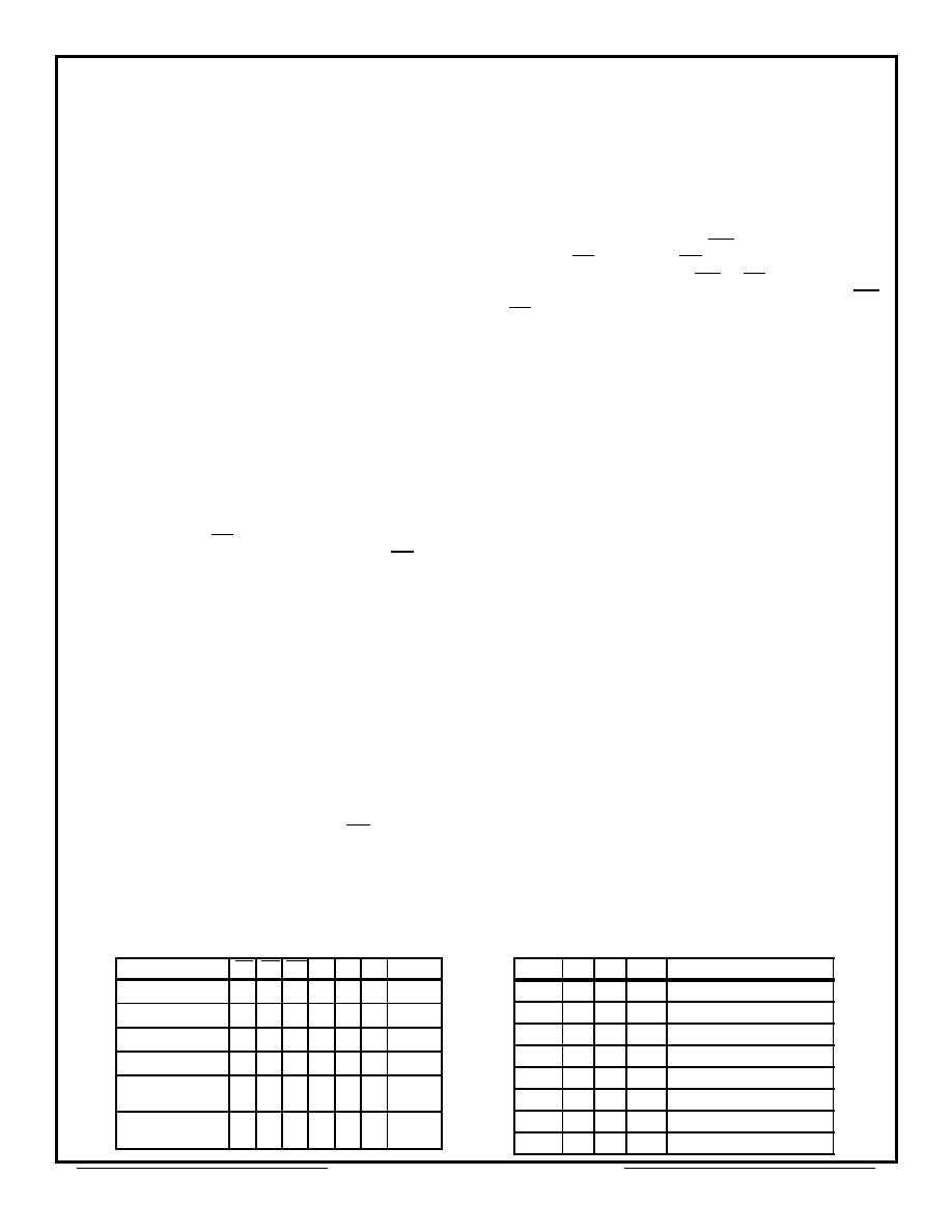
Table 1 ≠ Bus Operations
Operation
CE OE WE A0 A1 A9
I/O
READ
L
L
H
A
0
A
1
A
9
DOUT
STANDBY
H
X
X
X
X
X
HIGH Z
OUTPUT DISABLE
L
H
H
X
X
X
HIGH Z
WRITE
L
H
L
A
0
A
1
A
9
D
IN
ENABLE SECTOR
PROTECT
L
V
ID
L
X
X
V
ID
X
VERIFY SECTOR
PROTECT
L
L
H
L
H
V
ID
Code
Table 2 ≠ Sector Addresses Table
A16 A15
A14
Address Range
SA0
0
0
0
00000h ≠ 03FFFh
SA1
0
0
1
04000h ≠ 07FFFh
SA2
0
1
0
08000h ≠ 0BFFFh
SA3
0
1
1
0C000h ≠ 0FFFFh
SA4
1
0
0
10000h ≠ 13FFFh
SA5
1
0
1
14000h ≠ 17FFFh
SA6
1
1
0
18000h ≠ 1BFFFh
SA7
1
1
1
1C000h ≠ 1FFFFh