CIRCUIT TECHNOLOGY
www.aeroflex.com
eroflex Circuit Technology - Advanced Multichip Modules © SCD3750 REV A 8/31/98
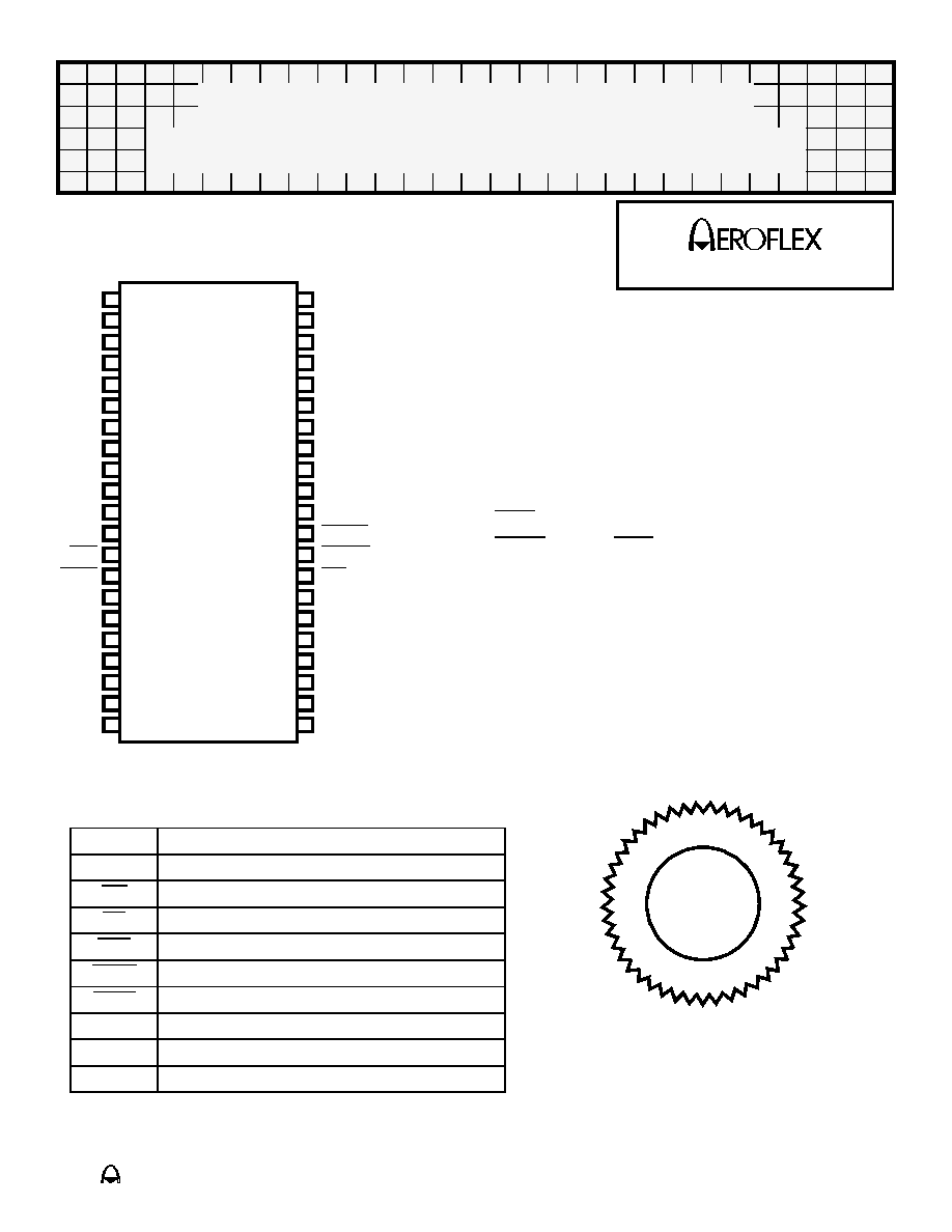
Pin Description
A
0≠9
Address Inputs
I/O
0-15
Data Input / Output
WE
Read/Write Enable
OE
Output Enable
RAS
Row Address Strobe
UCAS
Upper Byte Control / Column Address Strobe
LCAS
Lower Byte Control / Column Address Strobe
V
CC
+5.0V Power Supply
V
SS
Ground
NC
Not Connected
Features
s
Fast Access Time (t
RAC
): 70ns
s
Power Supply: 5.0V
±
0.5V
s
Packaging
q
42 Lead Plastic Surface-Mount SOJ (L4)
s
Industrial and Military Temperature Ranges
s
Three-State Unlatched Output
s
Fast Page Mode
s
RAS-Only Refresh
s
xCAS Before RAS Refresh
s
Hidden Refresh
s
1024 Cycle Refresh in 16ms
s
Low Power Dissipation
s
Long Refresh Period Option
ACT≠PD1M16 Fast Page Mode
16 Megabit Plastic Monolithic DRAM
F
I
E
I
D
C
E
R T
A
E
R
O
F
L E
X L A
B
S
I
N
C
.
ISO
9001
V
SS
I/O15
I/O14
I/O13
I/O12
V
SS
I/O11
I/O10
I/O9
I/O8
NC
LCAS
UCAS
OE
A9
A8
A7
A6
A5
A4
V
SS
Vcc
I/O0
I/O1
I/O2
I/O3
Vcc
I/O4
I/O5
I/O6
I/O7
NC
NC
WE
RAS
NC
NC
A0
A1
A2
A3
Vcc
42
41
40
39
38
37
36
35
34
33
32
31
30
29
28
27
26
25
24
23
22
1
2
3
4
5
6
7
8
9
10
11
12
13
14
15
16
17
18
19
20
21
Pin Configuration
Top View
Aeroflex Circuit Technology
SCD3750 REV A 8/31/98 Plainview NY (516) 694-6700
2
Absolute Maximum Ratings
Symbol
Parameter
MINIMUM
MAXIMUM
Units
T
C
Case Operating Temp.
-55
+125
∞C
T
STG
Storage Temperature
-55
+150
∞C
I
OS
Short Circuit Output Current
-
50
mA
P
T
Power Dissipated
-
1
W
V
CC
Supply Voltage Range
-1.0
+7.0
V
V
T
Voltage Range on any Pin*
-1.0
+7.0
V
Stresses beyond those listed under "absolute maximum ratings" may cause permanent damage to the device. These are
stress ratings only, and functional operation of the device at these or any other conditions beyond those indicated under
"recommended operating conditions" is not implied. Exposure to absolute-maximum rated conditions for extended periods may
affect device reliability.
* All voltage values are with respect to Vss.
Recommended Operating Conditions
Symbol
Parameter
Minimum
Maximum
Units
V
CC
Power Supply Voltage
+4.5
+5.5
V
V
IH
Input High Voltage
+2.4
-
V
V
IL
Input Low Voltage
-
+0.8
V
T
CM
Operating Temp. (Mil)
-55
+125
∞C
T
CI
Operating Temp. (Ind.)
-40
+85
∞C
Capacitance
(V
IN
= 0V, f = 1MHz, Tc = 25∞C
)
Symbol
Parameter
Maximum
Units
C
I(A)
A
0-9
Input Capacitance
10
pF
C
I(RC)
RAS and CAS Input Capacitance
10
pF
C
I(OE)
OE Input Capacitance
10
pF
C
I(WE)
WE Input Capacitance
10
pF
C
O
Output Capacitance
15
pF
These parameters are guaranteed by design but not tested.
DC Characteristics
(V
CC
= 5.0V, V
SS
= 0V, T
CI
or T
CM
)
Parameter
Sym
Conditions
Min Max
Units
Output Low Voltage
V
OL
I
OL
= 4.2 mA
-
0.4
V
Output High Voltage
V
OH
I
OH
= -5 mA
2.4
V
Input Leakage Current
I
L
V
I
= 0 to +6.5V, All others 0V to V
CC
-10
+10
µA
Output Leakage Current
I
O
V
O
= 0 to V
CC,
CAS high
-10
+10
µA
Read or Write Cycle Current
1,2
I
CC1
V
CC
= 5.5V, minimum cycle
190
mA
Aeroflex Circuit Technology
SCD3750 REV A 8/31/98 Plainview NY (516) 694-6700
3
Standby Current
I
CC2
VIH = 2.4V (TTL), After 1 memory cycle,
RAS and CAS high
-
2
mA
I
CC3
VIH = Vcc - 0.05V (CMOS), After 1 memory
cycle, RAS and CAS high
-
1
mA
Average Page Current
2
I
CC4
RAS low, CAS cycling
-
100
mA
1. Measured with a maximum of one address change while RAS = V
IL
.
2. Measured with a maximum of one address change while CAS = V
IH.
AC Characteristics
*
(V
CC
= 5.0V ±10%, V
SS
= 0V, T
CI
or T
CM
)
Parameter
Sym
Min Max
Units
Access Time from Column-Address
t
AA
-
35
ns
CAS Low Access Time from CAS
t
CAC
-
20
ns
Column Access Time from CAS Precharge
t
CPA
-
40
ns
Access Time from RAS
t
RAC
-
70
ns
OE Access Time
t
OEA
-
20
ns
Output Buffer Turn-off Delay
1
t
OFF
0
15
ns
Output Buffer Turn-off Delay Time from OE
1
t
OEZ
0
15
ns
* Valid data is presented at the outputs after all access times are satisfied but can go from the high-impedance
state to an invalid-data state prior to the specified access times as the outputs are driven when CAS goes low.
1. t
OFF
and t
OEZ
are specified when the outputs are no longer driven. The outputs are disabled by bringing either
OE or CAS high.
AC Characteristics
(V
CC
= 5.0V, V
SS
= 0V, T
CI
or T
CM
)
Parameter
Sym
Min Max
Units
Cycle Time, Read or Write Random
1
t
RC
130
-
ns
Cycle Time, Fast Page Mode Read or Write
1,2
t
PC
45
-
ns
Cycle Time, Fast Page Mode Read-Modify-Write
1
t
PRWC
90
-
ns
Pulse Duration, RAS Low Fast Page Mode
3
t
RASP
70
200,000
ns
Pulse Duration, RAS Low Nonpage Mode
3
t
RAS
70
10,000
ns
Pulse Duration, CAS Low
4
t
CAS
20
10,000
ns
Pulse Duration, CAS High Precharge Time
t
CP
10
-
ns
Pulse Duration, RAS High Precharge Time
t
RP
50
-
ns
Pulse Duration, WE Low
t
WP
15
-
ns
Setup Time, Column Address before CAS Low
t
ASC
0
-
ns
Setup Time, Row Address before RAS Low
t
ASR
0
-
ns
Setup Time, Data
5
t
DS
0
-
ns
Setup Time, WE High before CAS Low
t
RCS
0
-
ns
Setup Time, WE Low before CAS High
t
CWL
20
-
ns
Setup Time, WE Low before RAS High
t
RWL
20
-
ns
DC Characteristics (continued)
(V
CC
= 5.0V, V
SS
= 0V, T
CI
or T
CM
)
Parameter
Sym
Conditions
Min Max
Units

Aeroflex Circuit Technology
SCD3750 REV A 8/31/98 Plainview NY (516) 694-6700
4
Setup Time, WE Low before CAS Low (early-write operation only)
t
WCS
0
-
ns
Hold Time, Column Address after CAS Low
t
CAH
15
-
ns
Hold Time, Data
5
t
DH
15
-
ns
Hold Time, Row Address after RAS Low
t
RAH
10
-
ns
Hold Time, WE High after CAS High
6
t
RCH
0
-
ns
Hold Time, WE High after RAS High
6
t
RRH
0
-
ns
1. All cycle times assume t
T
= 5ns, reference to V
IH
(min) and V
IL
(max).
2. To assume t
PC
min, t
ASC
should be
t
CP
.
3. In read-write cycle, t
RWD
and t
RWL
must be observed.
4. In read-write cycle, t
CWD
and t
CWL
must be observed.
5. Referenced to the later of xCAS or WE in write operations.
6. Either t
RRH
or t
RCH
must be satisfied for a read cycle.
AC Characteristics
(V
CC
= 5.0V, V
SS
= 0V, T
CI
or T
CM
)
Parameter
Sym
Min Max
Units
WE Low before CAS Low Hold Time (early-write operation only)
t
WCH
15
-
ns
OE Command Hold Time
t
OEH
15
-
ns
RAS Referenced to OE Hold Time
t
ROH
10
-
ns
RAS from CAS Precharge (Fast Page Mode)
t
RHCP
40
-
ns
Column Address to WE Low Delay Time (read-write operation only)
t
AWD
60
-
ns
RAS Low to CAS High Delay Time (CBR refresh only)
t
CHR
15
-
ns
CAS High to RAS Low Delay Time (CAS to RAS Precharge Time)
t
CRP
5
-
ns
RAS Low to CAS High Delay Time (CAS Hold Time)
t
CSH
70
-
ns
CAS Low to RAS Low Delay Time (CAS Set-up Time)
t
CSR
5
-
ns
CAS Low to WE Low Delay Time (read-write operation only)
t
CWD
45
-
ns
OE to Data Delay Time
t
OED
15
-
ns
RAS Low to Column Address Delay Time
1
t
RAD
15
35
ns
Column Address to RAS High Delay Time
t
RAL
35
-
ns
RAS Low to CAS Low Delay Time
1
t
RCD
20
50
ns
RAS High to CAS Low Precharge Time
t
RPC
5
-
ns
CAS Low to RAS High Delay Time (RAS Hold Time)
t
RSH
20
-
ns
RAS Low to WE Low Delay Time (read-write operation only)
t
RWD
95
-
ns
WE Low after CAS Precharge Delay Time (read-write operation only)
t
CWD
65
-
ns
Refresh Time Interval
t
REF
16
ms
Transition time
2
t
T
3
50
ns
1. The maximum value is specified only to assure access time
2. Transition times (rise and fall) for RAS and xCAS are to be a minimum of 3ns and a maximum of 30ns.
AC Characteristics (continued)
(V
CC
= 5.0V, V
SS
= 0V, T
CI
or T
CM
)
Parameter
Sym
Min Max
Units

Aeroflex Circuit Technology
SCD3750 REV A 8/31/98 Plainview NY (516) 694-6700
5
I
OL
Parameter
Typical
Units
Input Pulse Level
0 ≠ 3.0
V
Input Rise and Fall
5
ns
Input and Output Reference Level
1.5
V
Output Timing Reference Level
1.5
V
Notes: 1) V
Z
is programmable from -2V to +7V.
2) I
OL
and I
OH
programmable from 0 to 16 mA.
3) Tester Impedance Z
O
= 75
.
4)
V
Z
is typically the midpoint of V
OH
and V
OL
.
5) I
OL
and I
OH
are adjusted to simulate a typical resistance load circuit.
6) ATE Tester includes jig capacitance.
I
OH
To Device Under Test
V
Z
~ 1.5 V (Bipolar Supply)
Current Source
Current Source
C
L
=
50 pF
AC Test Circuit