
FEATURES
eroflex Circuit Technology - Advanced Multichip Modules © SCD1663 REV A 4/28/98
CIRCUIT TECHNOLOGY
www.aeroflex.com
s
2 ≠ 512K x 8 SRAMs & 2 ≠ 512K x 8 Flash Die in
One MCM
s
Access Times of 25ns (SRAM) and 60ns (Flash) or
35ns (SRAM) and 70 or 90ns (Flash)
s
512K x 16 SRAM
s
512K x 16 5V Flash
s
Organized as 512K x 16 of SRAM and 512K x 16 of
Flash Memory with Separate Data Buses
s
Both Blocks of Memory are User Configurable as
1M x 8
s
Low Power CMOS
s
Input and Output TTL Compatible Design
s
MIL-PRF-38534 Compliant MCMs Available
s
Decoupling Capacitors and Multiple Grounds for Low
Noise
s
Industrial and Military Temperature Ranges
s
Industry Standard Pinouts
s
Packaging ≠ Hermetic Ceramic
q
66 Pin, 1.08" x 1.08" x .160" PGA Type, No Shoulder,
Aeroflex code# "P3"
q
66 Pin, 1.08" x 1.08" x .185" PGA Type, With
Shoulder, Aeroflex code# "P7"
q
68 Lead, .94" x .94" x .140" Single-Cavity Small
Outline Gull Wing, Aeroflex code# "F18" (Drops into
the 68 Lead JEDEC .99"SQ CQFJ footprint)
s
DESC SMD Pending ≠ 5962-96901
FLASH MEMORY FEATURES
s
Sector Architecture (Each Die)
q
8 Equal Sectors of 64K bytes each
q
Any combination of sectors can be erased with one
command sequence.
s
+5V Programing, 5V ±10% Supply
s
Embedded Erase and Program Algorithms
s
Hardware and Software Write Protection
s
Internal Program Control Time.
s
10,000 Erase / Program Cycles
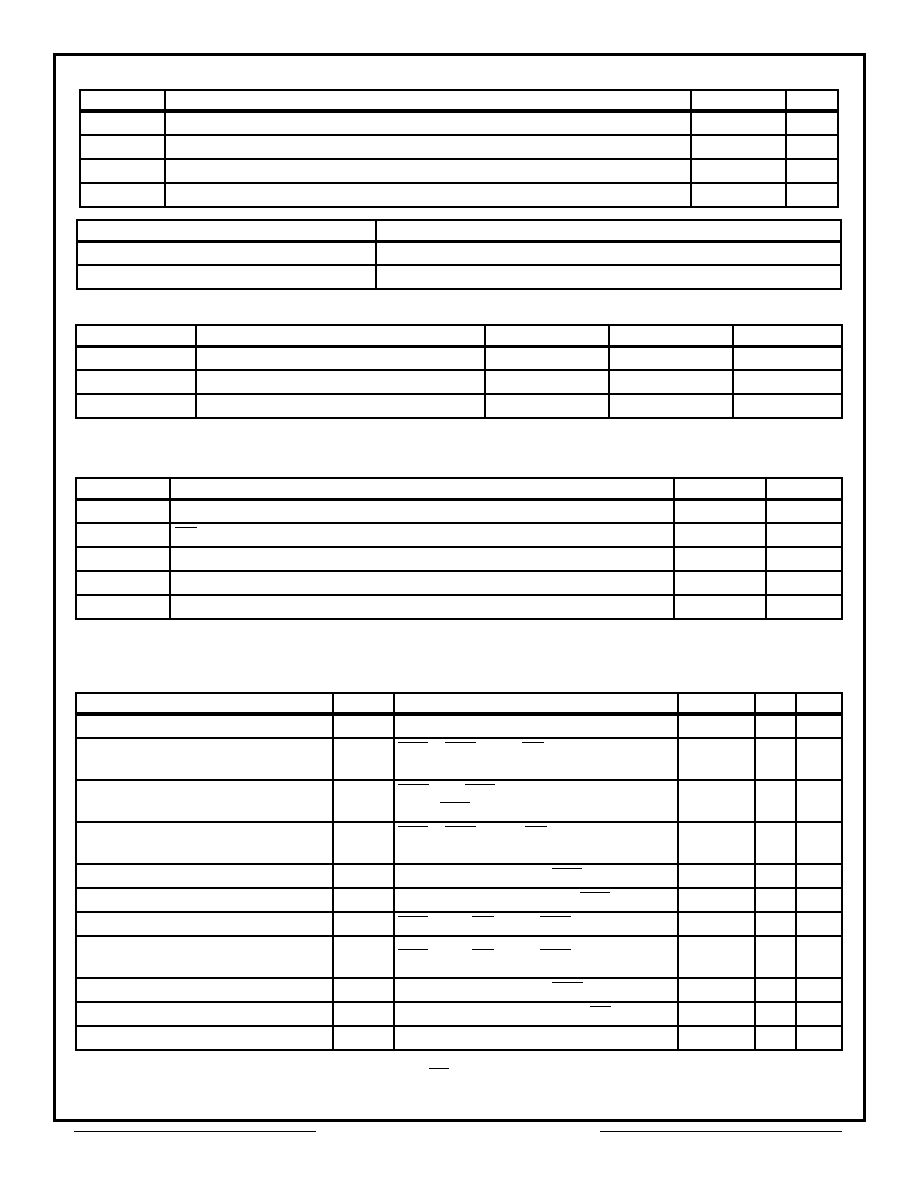
Pin Description
FI/O
0-15
Flash Data I/O
SI/O
0-15
SRAM Data I/O
A
0≠18
Address Inputs
FWE
1-2
Flash Write Enables
SWE
1-2
SRAM Write Enables
FCE
1-2
Flash Chip Enables
SCE
1-2
SRAM Chip Enables
OE
Output Enable
NC
Not Connected
V
CC
Power Supply
GND
Ground
512Kx8
FCE
2
OE
A
0
≠
A
18
SI/O
0-7
SI/O
8-15
FI/O
0-7
FI/O
8-15
8
8
8
8
FCE
1
FWE
2
FWE
1
SWE
2
SWE
1
SCE
1
SCE
2
Block Diagram ≠ PGA Type Packages (P3 & P7) & CQFP (F18)
SRAM
512Kx8
SRAM
512Kx8
Flash
512Kx8
Flash
512Kx16 SRAM/FLASH Multichip Module
ACT≠SF512K16 High Speed
Note: Programming information available upon request
Aeroflex Circuit Technology
SCD1663 REV A 4/28/98 Plainview NY (516) 694-6700
2
Absolute Maximum Ratings
Symbol
Rating
Range
Units
T
C
Operating Temperature
-55 to +125
∞C
T
STG
Storage Temperature
-65 to +150
∞C
V
G
Maximum Signal Voltage to Ground
-0.5 to +7
V
T
L
Maximum Lead Temperature (10 seconds)
300
∞C
Parameter
Flash Data Retention
10 Years
Flash Endurance (Write/Erase Cycles)
10,000
Normal Operating Conditions
Symbol
Parameter
Minimum
Maximum
Units
V
CC
Power Supply Voltage
+4.5
+5.5
V
V
IH
Input High Voltage
+2.2
V
CC
+ 0.3
V
V
IL
Input Low Voltage
-0.5
+0.8
V
Capacitance
(V
IN
= 0V, f = 1MHz, T
C
= 25∞C
)
Symbol
Parameter
Maximum
Units
C
AD
A
0
≠
A
18
Capacitance
50
pF
C
OE
OE Capacitance
50
pF
C
WE
1,2
F/S Write Enable Capacitance
20
pF
C
CE
1,2
F/S Chip Enable Capacitance
20
pF
C
I
/
O
I/O
0
≠ I/O
15
Capacitance
20
pF
These parameters are guaranteed by design but not tested
DC Characteristics
(V
CC
= 5.0V, V
SS
= 0V, Tc = -55∞C to +125∞C, unless otherwise indicated)
Parameter
Sym
Conditions
Min
Max Units
Input Leakage Current
I
LI
V
CC
= Max, V
IN
= 0 to V
CC
10
µA
Output Leakage Current
I
LO
FCE = SCE = V
IH
, OE = V
IH,
V
OUT
= 0 to V
CC
10
µA
SRAM Operating Supply Current x 16
Mode
I
CC
x16
SCE = V
IL
, OE = V
IH
, f = 5MHz, V
CC
=
Max, FCE = V
IH
260
mA
Standby Current
I
SB
FCE = SCE = V
IH
,
OE = V
IH
, f = 5MHz,
V
CC
= Max
35
mA
SRAM Output Low Voltage
V
OL
I
OL
= 8 mA, V
CC
= Min, FCE = V
IH
0.4
V
SRAM Output High Voltage
V
OH
I
OH
= -4.0 mA, , V
CC
= Min, FCE = V
IH
2.4
V
Flash Vcc Active Current for Read (1)
I
CC1
FCE = V
IL
, OE = V
IH
, SCE = V
IH
130
mA
Flash Vcc Active Current for Program
or Erase (2)
I
CC2
FCE = V
IL
, OE = V
IH
, SCE = V
IH
150
mA
Flash Output Low Voltage
V
OL
I
OL
= 8 mA, V
CC
= Min, SCE = V
IH
0.45
V
Flash Output High Voltage
V
OH
I
OH
= -2.5 mA, , V
CC
= Min, SCE = V
IH
0.85 x V
CC
V
Flash Low Vcc Lock Out Voltage
V
LKO
3.2
4.2
V
Notes: 1) The I
CC
current listed includes both the DC operating current and the frequency dependent component (at 5MHz). The
frequency component typically is less than 2mA/MHz, with OE at V
IH
2) I
CC
active while Embedded Algorithim (program or
erase) is in progress 3) DC test conditions: V
IL
= 0.3V, V
IH
= V
CC
- 0.3V

Aeroflex Circuit Technology
SCD1663 REV A 4/28/98 Plainview NY (516) 694-6700
3
SRAM AC Characteristics
(V
CC
= 5.0V, V
SS
= 0V, Tc= -55∞C to +125∞C)
Read Cycle
Parameter
Symbol
≠025
Min Max
≠035
Min Max
Units
Read Cycle Time
t
RC
25
35
ns
Address Access Time
t
AA
25
35
ns
Chip Select Access Time
t
ACE
25
35
ns
Output Hold from Address Change
t
OH
0
0
ns
Output Enable to Output Valid
t
OE
12
25
ns
Chip Select to Output in Low Z *
t
CLZ
2
4
ns
Output Enable to Output in Low Z *
t
OLZ
0
0
ns
Chip Deselect to Output in High Z *
t
CHZ
12
15
ns
Output Disable to Output in High Z *
t
OHZ
12
15
ns
* Parameters guaranteed by design but not tested
Write Cycle
Parameter
Symbol
≠025
Min Max
≠035
Min Max
Units
Write Cycle Time
t
WC
25
35
ns
Chip Select to End of Write
t
CW
17
25
ns
Address Valid to End of Write
t
AW
17
25
ns
Data Valid to End of Write
t
DW
13
20
ns
Write Pulse Width
t
WP
17
25
ns
Address Setup Time
t
AS
2
2
ns
Output Active from End of Write *
t
OW
4
4
ns
Write to Output in High Z *
t
WHZ
13
15
ns
Data Hold from Write Time
t
DH
0
0
ns
Address Hold Time
t
AH
0
0
ns
* Parameters guaranteed by design but not tested
Truth Table
Mode
SCE
OE
SWE
Data I/O
Power
Standby
H
X
X
High Z
Standby
Read
L
L
H
Data Out
Active
Output Disable
L
H
H
High Z
Active
Write
L
X
L
Data In
Active

Aeroflex Circuit Technology
SCD1663 REV A 4/28/98 Plainview NY (516) 694-6700
4
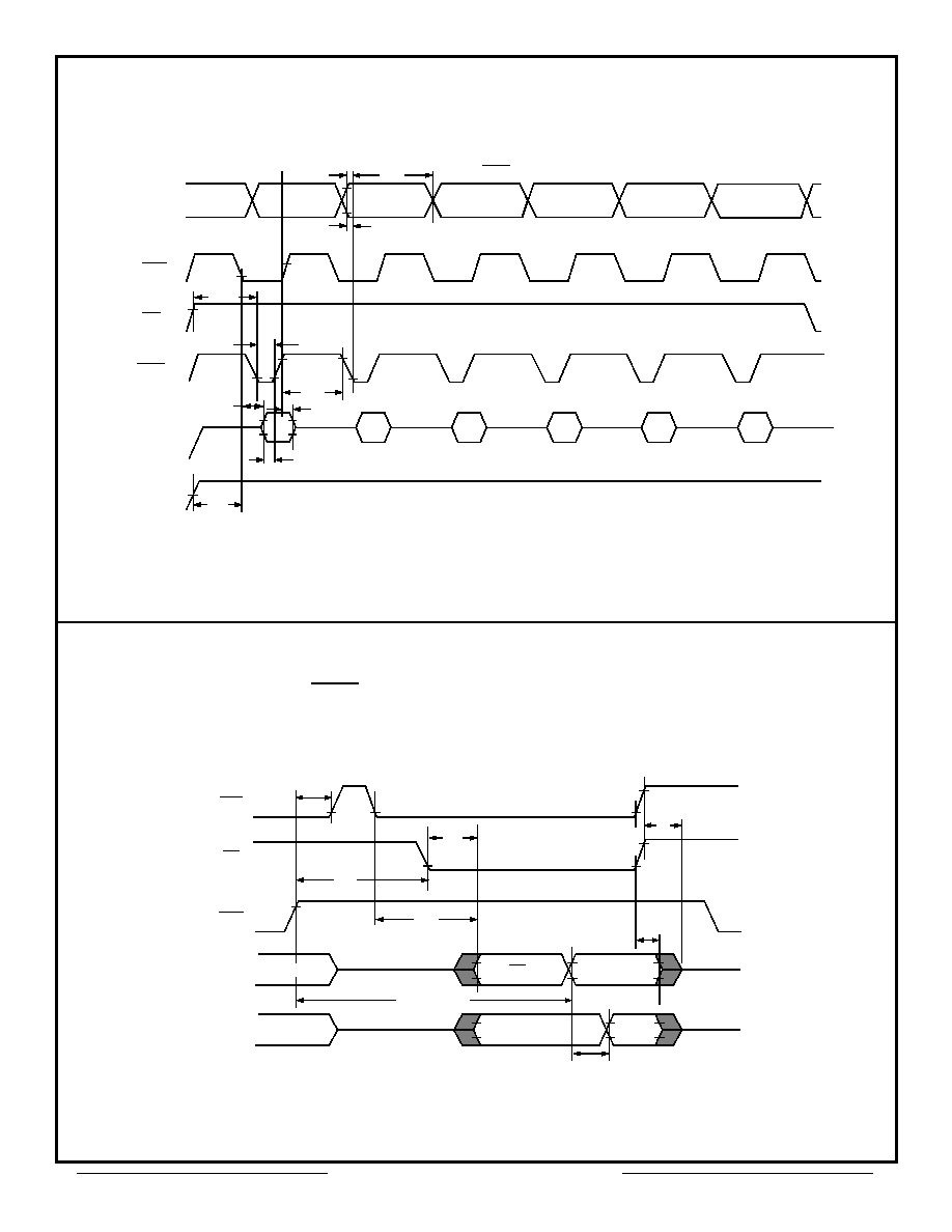
Timing Diagrams -- SRAM
D
I/O
t
RC
t
OH
t
AA
Data Valid
Previous Data Valid
t
OE
High Z
t
OHZ
Read Cycle Timing Diagrams
Data Valid
t
CLZ
SCE
OE
t
ACE
t
CHZ
UNDEFINED
DON'T CARE
Read Cycle 2 (SWE = V
IH
)
Write Cycle (SCE Controlled, OE = V
IH
)
t
CW
t
AS
t
WP
t
DW
t
OW
SCE
SWE
Data Valid
Write Cycle (SWE Controlled, OE = V
IH
)
D
I/O
AC Test Circuit
I
OL
Parameter
Typical
Units
Input Pulse Level
0 ≠ 3.0
V
Input Rise and Fall
5
ns
Input and Output Timing Reference
1.5
V
Notes:
1) V
Z
is programmable from -2V to +7V. 2) I
OL
and I
OH
programmable from 0 to 16 mA. 3) Tester Impedance
Z
O
= 75
. 4)
V
Z
is typically the midpoint of V
OH
and V
OL
. 5) I
OL
and I
OH
are adjusted to simulate a typical resistance
load circuit. 6) ATE Tester includes jig capacitance.
I
OH
To Device Under Test
V
Z
~ 1.5 V (Bipolar Supply)
Current Source
Current Source
C
L
= 50 pF
t
WC
t
AW
t
AH
t
RC
t
AA
t
OLZ
S
EE
N
OTE
S
EE
N
OTE
S
EE
N
OTE
S
EE
N
OTE
Note: Guaranteed by design, but not tested.
D
I/O
t
DH
t
WHZ
S
EE
N
OTE
Read Cycle 1 (SCE = OE = V
IL
, SWE = V
IH
)
Write Cycle Timing Diagrams
t
WP
t
DW
Data Valid
t
WC
t
AW
t
AH
D
I/O
t
DH
SCE
SWE
t
CW
t
AS
A
0-18
A
0-18
A
0-18
A
0-18
AC Test Conditions

Aeroflex Circuit Technology
SCD1663 REV A 4/28/98 Plainview NY (516) 694-6700
5
Flash AC Characteristics ≠ Read Only Operations
(Vcc = 5.0V, Vss = 0V, Tc = -55∞C to +125∞C)
Parameter
Symbol
JEDEC Stand'd
≠60
Min Max
≠70
Min Max
≠90
Min Max
Units
Read Cycle Time
t
AVAV
t
RC
60
70
90
ns
Address Access Time
t
AVQV
t
ACC
60
70
90
ns
Chip Enable Access Time
t
ELQV
t
CE
60
70
90
ns
Output Enable to Output Valid
t
GLQV
t
OE
30
35
35
ns
Chip Enable to Output High Z (1)
t
EHQZ
t
DF
20
20
20
ns
Output Enable High to Output High Z(1)
t
GHQZ
t
DF
20
20
20
ns
Output Hold from Address, CE or OE Change, Whichever is First
t
AXQX
t
OH
0
0
0
ns
Note 1. Guaranteed by design, but not tested
Flash AC Characteristics ≠ Write / Erase / Program Operations, FWE Controlled
(Vcc = 5.0V, Vss = 0V, Tc = -55∞C to +125∞C)
Parameter
Symbol
JEDEC Stand'd
≠60
Min Max
≠70
Min Max
≠90
Min Max
Units
Write Cycle Time
t
AVAC
t
WC
60
70
90
ns
Chip Enable Setup Time
t
ELWL
t
CE
0
0
0
ns
Write Enable Pulse Width
t
WLWH
t
WP
40
45
45
ns
Address Setup Time
t
AVWL
t
AS
0
0
0
ns
Data Setup Time
t
DVWH
t
DS
40
45
45
ns
Data Hold Time
t
WHDX
t
DH
0
0
0
ns
Address Hold Time
t
WLAX
t
AH
45
45
45
ns
Write Enable Pulse Width High
t
WHWL
t
WPH
20
20
20
ns
Duration of Byte Programming Operation
t
WHWH
1
14
TYP
14
TYP
14
TYP
µs
Sector Erase Time
t
WHWH
2
30
30
30
Sec
Read Recovery Time before Write
t
GHWL
0
0
0
µs
Vcc Setup Time
t
VCE
50
50
50
µs
Chip Programming Time
50
50
50
Sec
Chip Enable Hold Time
t
OEH
1
10
10
10
ns
Chip Erase Time
t
WHWH
3
120
120
120
Sec
1. Toggle and Data Polling only.
Flash AC Characteristics ≠ Write / Erase / Program Operations, FCE Controlled
(Vcc = 5.0V, Vss = 0V, Tc = -55∞C to +125∞C)
Parameter
Symbol
JEDEC Stand'd
≠60
Min Max
≠70
Min Max
≠90
Min Max
Units
Write Cycle Time
t
AVAC
t
WC
60
70
90
ns
Write Enable Setup Time
t
WLE
L
t
WS
0
0
0
ns
Chip Enable Pulse Width
t
ELEH
t
CP
40
45
45
ns
Address Setup Time
t
AVEL
t
AS
0
0
0
ns
Data Setup Time
t
DVEH
t
DS
40
45
45
ns
Data Hold Time
t
EHDX
t
DH
0
0
0
ns
Address Hold Time
t
ELAX
t
AH
45
45
45
ns
Chip Enable Pulse Width High
t
EHEL
t
CPH
20
20
20
ns
Duration of Byte Programming
t
WHWH
1
14
TYP
14
TYP
14
TYP
µs
Sector Erase Time
t
WHWH
2
30
30
30
Sec
Read Recovery Time
t
GHEL
0
0
0
ns
Chip Programming Time
50
50
50
Sec
Chip Erase Time
t
WHWH
3
120
120
120
Sec

Aeroflex Circuit Technology
SCD1663 REV A 4/28/98 Plainview NY (516) 694-6700
6
AC Waveforms for Flash Memory Read Operations
t
OH
t
CE
t
OE
t
ACC
t
RC
t
DF
Output Valid
High Z
High Z
Outputs
OE
FWE
FCE
Addresses
Addresses Stable
FWE
OE
FCE
Data
Addresses
5.0V
5555H
PA
Data Polling
PA
D7
D
OUT
PD
AOH
t
WHWH
1
t
OE
t
RC
t
CE
t
DF
t
OH
t
AH
t
AS
t
DH
t
WPH
t
WP
t
DS
t
CE
t
WC
Write/Erase/Program
Operation for Flash Memory, FWE Controlled
Notes:
1. PA is the address of the memory location to be programmed.
2. PD is the data to be programmed at byte address.
3. D7 is the 0utput of the complement of the data written to the deviced.
4. Dout is the output of the data written to the device.
5. Figure indicates last two bus cycles of four bus cycle sequence.
t
GHWL
Aeroflex Circuit Technology
SCD1663 REV A 4/28/98 Plainview NY (516) 694-6700
7
AC Waveforms Chip/Sector
Erase Operations for Flash Memory
Data
Addresses
V
CC
5555H
Data Polling
t
AH
FCE
t
AS
FWE
5555H
5555H
SA
2AAAH
2AAAH
t
GHWL
t
WP
t
WPH
t
DS
t
DH
t
CE
t
VCE
55H
AAH
80H
55H
10H/30H
AAH
OE
Notes:
1. SA is the sector address for sector erase.
AC Waveforms for Data Polling
During Embedded Algorithm Operations for Flash Memory
t
OE
t
CH
t
WHWH
1 or 2
t
OE
t
OH
t
DF
t
CE
t
OEH
*
* DQ7=Valid Data (The device has completed the Embedded operation).
DQ0≠DQ6=Invalid
DQ7
DQ7=
Valid Data
DQ0≠DQ6
Valid Data
High Z
FCE
DQ7
OE
FWE
DQ0-DQ6

Aeroflex Circuit Technology
SCD1663 REV A 4/28/98 Plainview NY (516) 694-6700
8
FWE
OE
FCE
Data
Addresses
5.0V
5555H
PA
Data Polling
PA
D7
D
OUT
PD
AOH
t
WHWH
1
t
AH
t
AS
t
DH
t
CPH
t
CP
t
DS
t
WS
t
WC
t
GHWL
Notes:
1. PA is the address of the memory location to be programmed.
2. PD is the data to be programmed at byte address.
3. D7 is the 0utput of the complement of the data written to the device.
4. D
OUT
is the output of the data written to the device.
5. Figure indicates last two bus cycles of four bus cycle sequence.
Write/Erase/Program Operation for Flash Memory, FCE Controlled

Aeroflex Circuit Technology
SCD1663 REV A 4/28/98 Plainview NY (516) 694-6700
9
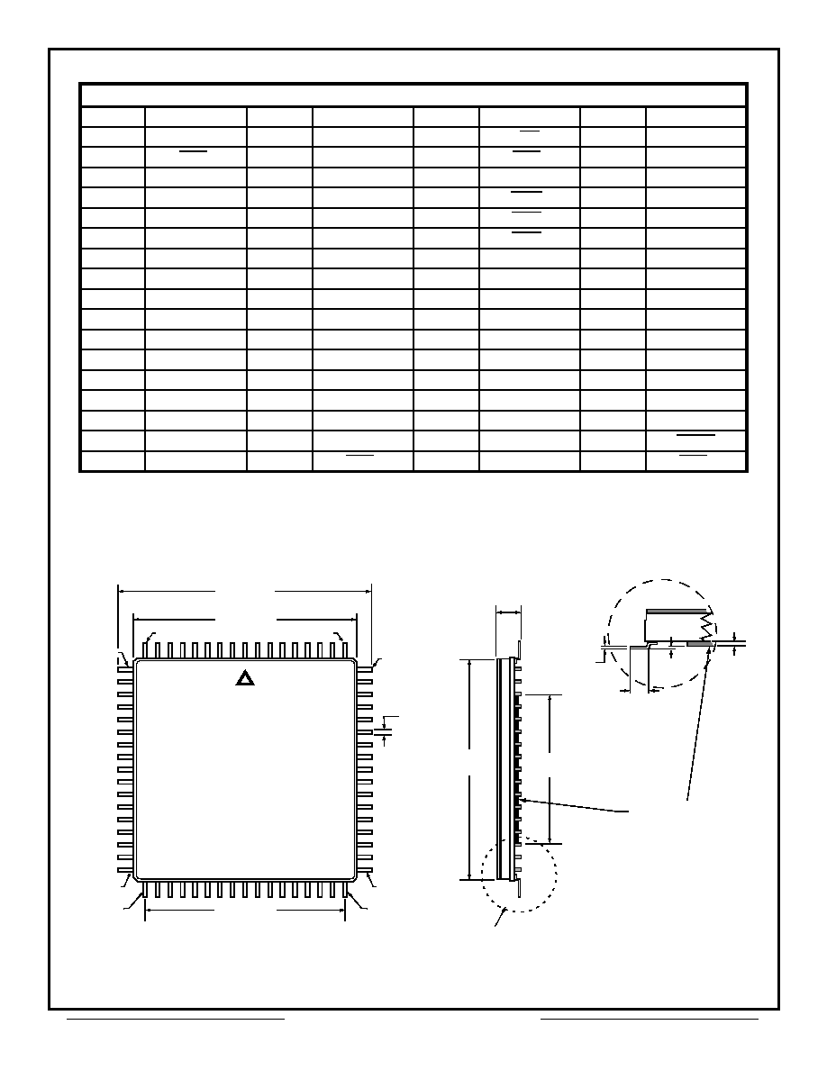
Pin Numbers & Functions
66 Pins -- PGA-Type
Pin #
Function
Pin #
Function
Pin #
Function
Pin #
Function
1
SI/O
8
18
A
12
35
FI/O
9
52
FWE
1
2
SI/O
9
19
Vcc
36
FI/O
10
53
FCE
1
3
SI/O
10
20
SCE
1
37
A
6
54
GND
4
A
13
21
NC
38
A
7
55
FI/O
3
5
A
14
22
SI/O
3
39
NC
56
FI/O
15
6
A
15
23
SI/O
15
40
A
8
57
FI/O
14
7
A
16
24
SI/O
14
41
A
9
58
FI/O
13
8
A
18
25
SI/O
13
42
FI/O
0
59
FI/O
12
9
SI/O
0
26
SI/O
12
43
FI/O
1
60
A
0
10
SI/O
1
27
OE
44
FI/O
2
61
A
1
11
SI/O
2
28
A
17
45
V
CC
62
A
2
12
SWE
2
29
SWE
1
46
FCE
2
63
FI/O
7
13
SCE
2
30
SI/O
7
47
FWE
2
64
FI/O
6
14
GND
31
SI/O
6
48
FI/O
11
65
FI/O
5
15
SI/O
11
32
SI/O
5
49
A
3
66
FI/O
4
16
A
10
33
SI/O
4
50
A
4
17
A
11
34
FI/O
8
51
A
5
All dimensions in inches
1.085 SQ
1.000
.600
1.000
.100
.020
.016
.100
.180
TYP
1.030
1.040
.160
Pin 56
Pin 66
Pin 11
Pin 1
Bottom View (P7 & P3)
MAX
MAX
"P3" -- 1.08" SQ PGA Type (without shoulder) Package
"P7" -- 1.08" SQ PGA Type (with shoulder) Package
1.030
1.040
.020
.016
.100
.025
.185
MAX
Side View
(P7)
Side View
(P3)
.050
.180
TYP
.035
Aeroflex Circuit Technology
SCD1663 REV A 4/28/98 Plainview NY (516) 694-6700
10
Pin Numbers & Functions
68 Pins -- Dual-Cavity CQFP
Pin #
Function
Pin #
Function
Pin #
Function
Pin #
Function
1
GND
18
GND
35
OE
52
GND
2
FCE
1
19
SI/O
8
36
SCE
2
53
FI/O
7
3
A
5
20
SI/O
9
37
A
17
54
FI/O
6
4
A
4
21
SI/O
10
38
SWE
2
55
FI/O
5
5
A
3
22
SI/O
11
39
FWE
1
56
FI/O
4
6
A
2
23
SI/O
12
40
FWE
2
57
FI/O
3
7
A
1
24
SI/O
13
41
A
18
58
FI/O
2
8
A
0
25
SI/O
14
42
NC
59
FI/O
1
9
NC
26
SI/O
15
43
NC
60
FI/O
0
10
SI/O
0
27
V
cc
44
FI/O
15
61
V
CC
11
SI/O
1
28
A
11
45
FI/O
14
62
A
10
12
SI/O
2
29
A
12
46
FI/O
13
63
A
9
13
SI/O
3
30
A
13
47
FI/O
12
64
A
8
14
SI/O
4
31
A
14
48
FI/O
11
65
A
7
15
SI/O
5
32
A
15
49
FI/O
10
66
A
6
16
SI/O
6
33
A
16
50
FI/O
9
67
SWE1
17
SI/O
7
34
SCE
1
51
FI/O
8
68
FCE
2
.015
±.002
All dimensions in inches
"F18" -- CQFP Package
.015
.990 SQ
±.010
.940 SQ
±.010
.800 REF
See Detail "A"
±.002
Pin 60
Pin 44
Pin 43
Pin 27
Pin 26
Pin 10
Pin 9
.900 SQ
MAX
Pin 61
.140
REF
.640 SQ
REF
.008
±.002
Detail "A"
.010
±.008
.040
Metal spacer
Aeroflex Circuit Technology
SCD1663 REV A 4/28/98 Plainview NY (516) 694-6700
11
Ordering Information
Model Number
DESC SMD Number
Speed
Package
ACT≠SF512K16N≠26P3Q
5462-96901 (Pending)
25(S) / 60(F) ns
1.08"sq PGA-Type
ACT≠SF512K16N≠37P3Q
5462-96901 (Pending)
35(S) / 70(F) ns
1.08"sq PGA-Type
ACT≠SF512K16N≠39P3Q
5462-96901 (Pending)
35(S) / 90(F) ns
1.08"sq PGA-Type
ACT≠SF512K16N≠26P7Q
5462-96901 (Pending)
25(S) / 60(F) ns
1.08"sq PGA-Type
ACT≠SF512K16N≠37P7Q
5462-96901 (Pending)
35(S) / 70(F) ns
1.08"sq PGA-Type
ACT≠SF512K16N≠39P7Q
5462-96901 (Pending)
35(S) / 90(F) ns
1.08"sq PGA-Type
ACT≠SF512K16N≠26F18Q
5462-96901 (Pending)
25(S) / 60(F) ns
.94"sq CQFP
ACT≠SF512K16N≠37F18Q
5462-96901 (Pending)
35(S) / 70(F) ns
.94"sq CQFP
ACT≠SF512K16N≠39F18Q
5462-96901 (Pending)
35(S) / 90(F) ns
.94"sq CQFP
Note: (S) = Speed for SRAM, (F) = Speed for FLASH
Part Number Breakdown
ACT≠ S F 512K 16 N≠ 26 P7 Q
Aeroflex Circuit
Technology
Memory Type
S (SRAM) & F (FLASH) Combo
Memory Depth
Memory Width, Bits
Memory Speed Code
Package Type & Size
C = Commercial Temp, 0∞C to +70∞C
I = Industrial Temp, -40∞C to +85∞C
T = Military Temp, -55∞C to +125∞C
M = Military Temp, -55∞C to +125∞C, Screening
*
Q = MIL-PRF-38534 Compliant / SMD
Screening
*
Screened to the individual test methods of MIL-STD-883
Surface Mount Packages
Thru-Hole Packages
F18 = .94"SQ 68 Lead Dual-Cavity
CQFP
P3 = 1.085"SQ PGA 66 Pins
with out shoulder
P7 = 1.085"SQ PGA 66 Pins
with shoulder
26 = 25ns SRAM & 60ns FLASH
37 = 35ns SRAM & 70ns FLASH
39 = 35ns SRAM & 90ns FLASH
Options, N = none
Aeroflex Circuit Technology
35 South Service Road
Plainview New York 11830
Telephone: (516) 694-6700
FAX: (516) 694-6715
Toll Free Inquiries: 1-(800) 843-1553
C I R C U I T T E C H N O L O G Y
Specifications subject to change without notice.