 | –≠–ª–µ–∫—Ç—Ä–æ–Ω–Ω—ã–π –∫–æ–º–ø–æ–Ω–µ–Ω—Ç: ARX4868-2 | –°–∫–∞—á–∞—Ç—å:  PDF PDF  ZIP ZIP |
eroflex Circuit T
echnology
≠ Data Bus Modules For The Future © SCD4808 REV A 3/9/98
CIRCUIT TECHNOLOGY
www.aeroflex.com/act1.htm
Features
∑ ARX4808 Dual Transceiver meets
MIL-STD-1553A & B, Macair A3818, A5690, A5232
and A4905 specs
∑ Operates with ±12 V to ±15 V & +5 V Power Supplies
∑ Voltage source output for higher bus drive power
∑ Plug-in or Flat Package
∑ Monolithic construction using linear ASICs
∑ Low receiver data level version, ARX4868
∑ Processed and Screened to MIL-STD-883 specs
∑ DESC SMD (Standard Military Drawing ) Pending
General Description:
The Aeroflex Laboratories transceiver
model ARX4808 is a new generation
Dual monolithic transceiver which
provides full compliance with Macair
and MIL-STD-1553 data bus
requirements
The model ARX4808 performs the
front-end analog function of inputting
and outputting data through a
transformer to a MIL-STD-1553 or
Macair data bus. The ARX4808 can
be considered a "Universal"
Transceiver in that it is compatible
with MIL-STD-1553A & B, Macair
A-3818, A-4905, A-5232 and A-5690.
Design of this transceiver reflects
particular attention to active filter
performance. This results in low bit
and word error rate with superior
waveform purity and minimal zero
crossover distortion. The ARX4808
series active filter design has
additional high frequency roll-off to
provide the required Macair low
harmonic distortion waveform
without increasing the pulse delay
characteristics significantly.
Efficient transmitter electrical and
thermal design provides low internal
power dissipation and heat rise at
high and well as low duty cycles.The
receiver input threshold is set
Internally.
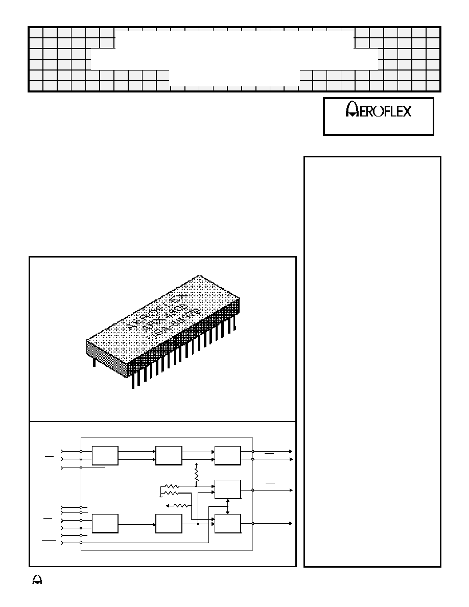
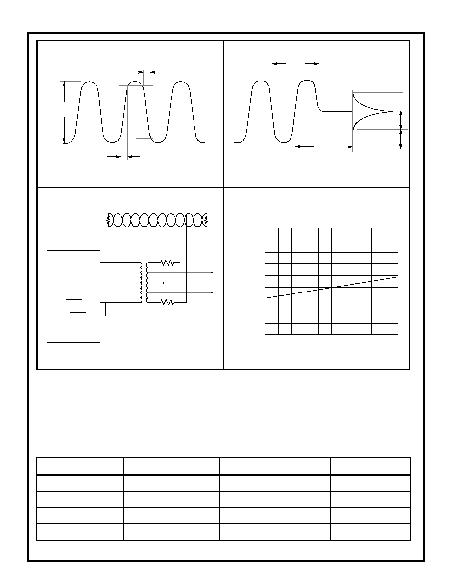
Transmitter
The Transmitter section accepts
bi-phase TTL data at the input and
when coupled to the data bus with a
1:1 transformer, isolated on the data
bus side with two 52.5 Ohm fault
isolation resistors, and loaded by two
70 Ohm terminations plus additional
ARX4808 Transceiver
Block Diagram (without Transformer), 1/2 of unit shown
SHAPING
OUTPUT
STAGE
COMP.
COMP.
ACTIVE
FILTER
INPUT
AMP
DRIVER
TX DATA IN
TX DATA IN
TX INHIBIT
+5 V
RX DATA IN
RX DATA IN
STROBE
TX DATA OUT
TX DATA OUT
RX DATA OUT
RX DATA OUT
V
EE
V
CC
V+
V-
ARX4808 Dual Transceivers for
MACAIR A3818, A5690, A5232, A4905
& MIL-STD-1553
Aeroflex Circuit Technology
SCD4808 REV A 3/9/98 Plainview NY (516) 694-6700
2
receivers, the data bus signal
produced is 7.5 volts minimum P-P
at A-A' (See Figure 5.). When both
DATA and DATA inputs are held low
or high, the transmitter output
becomes a high impedance and is
"removed" from the line. In addition,
an overriding "INHIBIT" input
provides for the removal of the
transmitter output from the line. A
logic "1" applied to the "INHIBIT"
takes priority over the condition of
the data inputs and disables the
transmitter. (See Transmitter Logic
Waveforms, Figure 1.)
The transmitter utilizes an active
filter to suppress harmonics above
1 MHz to meet Macair specifications
A-3818, A-4905, A-5232 and
A-5690. The transmitter may be
safely operated for an indefinite
period at 100% duty cycle into a
data bus short circuit.
Receiver
The Receiver section accepts
bi-phase differential data at the input
and produces two TTL signals at the
output. The outputs are DATA and
DATA, and represent positive and
negative excursions of the input
beyond a pre-determined threshold.
(See Receiver Logic Waveforms,
Figure 2.)
The internal threshold is nominally
set to detect data bus signals
exceeding 1.05 Volts P-P and
reject signals less than 0.6 volts
P-P when used with a 1:1 turns
ratio transformer. (See Figure 5
for transformer data and typical
connection.)
A low level at the Strobe input
inhibits the DATA and DATA
outputs. If unused, a 2K pull-up to
+5 Volts is recommended
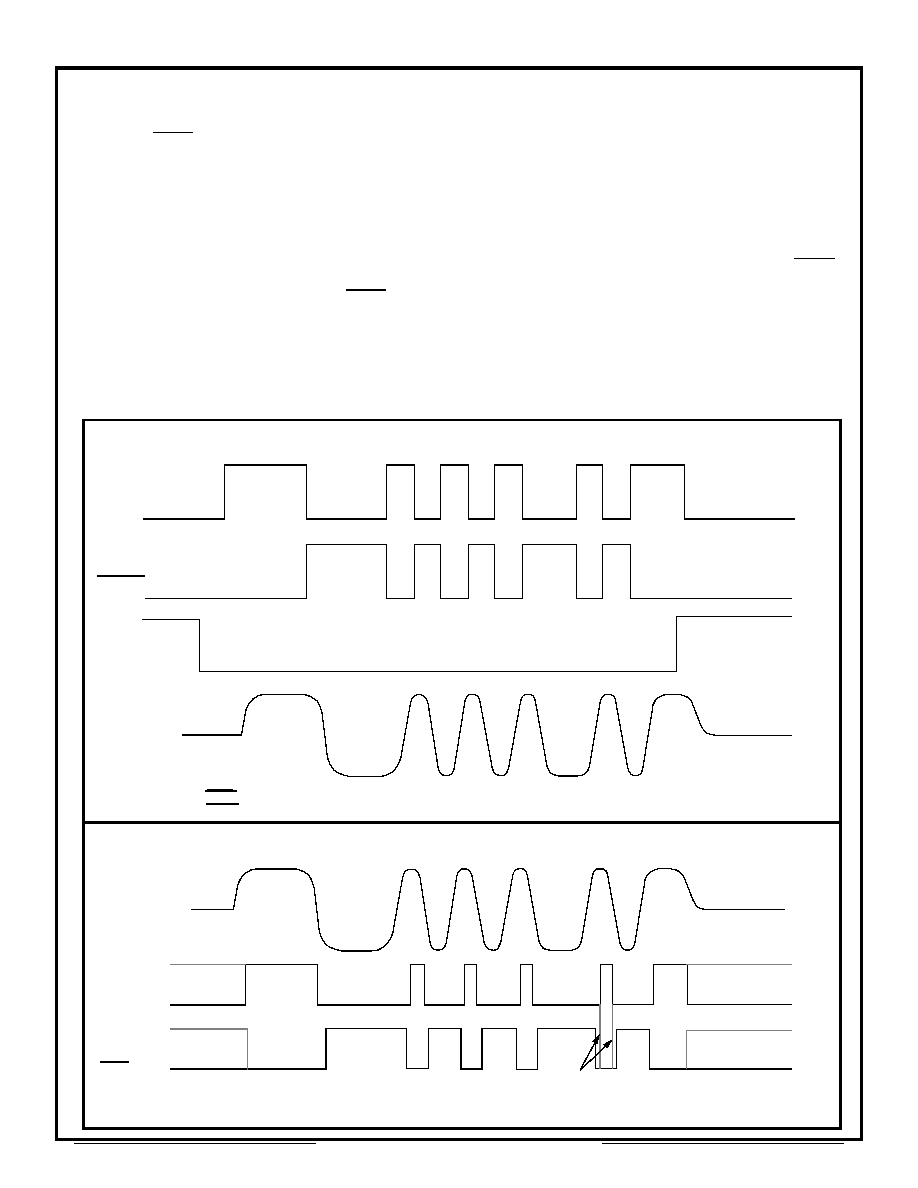
DATA IN
DATA IN
INHIBIT
LINE TO LINE
OUTPUT
NOTES:
2. DATA and DATA inputs must be complementary waveforms or 50% duty cycle average, with no delays between them.
3. DATA and DATA must be in the same state during off time (both high or low).
Figure 1 Transmitter Logic Waveforms
Figure 2 Receiver Logic Waveforms
Note overlap
NOTE
:
Waveforms shown are for normally low devices. For normally high receiver output
devices, the receiver outputs are swapped as shown by the dashed lines
level
LINE TO LINE
INPUT
DATA OUT
DATA OUT
1. Line to line waveforms illustrate Macair signals, MIL-STD-1553 signals are trapezoidal
Aeroflex Circuit Technology
SCD4808 REV A 3/9/98 Plainview NY (516) 694-6700
3
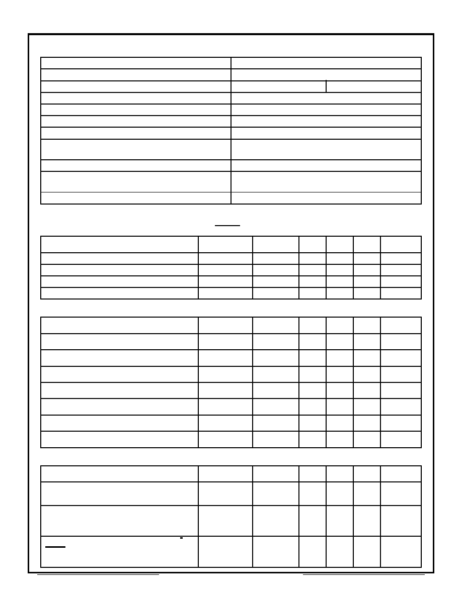
Absolute Maximum Ratings, Per Channel
Operating case temperature
-55∞C to +125∞C
Storage case temperature
-65∞C to +150 ∞C
Power supply Voltages
±15 V P.S. to ±18V MAX
+5 V P.S. to +7V MAX
Logic input Voltage
-0.3 V to +5.5 V
Receiver differential input
±40 V
Receiver input voltage (common mode)
±10V
Driver peak output current
300 mA
Total package power dissipation over the full operating
case temperature range
2.4 Watts
Power Dissipation for hottest die, (100% duty cycle)
600 mW
Maximum junction to case temperature rise for the hot-
test device (100 % duty cycle)
36∞C
Junction-Case, Thermal resistance for hottest device
60∞C/W
Electrical Characteristics Per Channel, Transmitter Section
Input Characteristics, TX DATA in or TX DATA in
Parameter
Condition
Symbol
Min
Typ
Max
Unit
"0" Input Current
V
IN
= 0.4 V
I
ILD
-0.2
-0.4
mA
"1" Input Current
V
IN
= 2.7 V
I
IHD
1.0
40
µA
"0" Input Voltage
V
IHD
0.7
V
"1" Input Voltage
V
IHD
2.0
V
Inhibit Characteristics
"0" Input Current
V
IN
=0.4V
I
ILI
-0.2
-0.4
mA
"1" Input Current
V
IN
=2.7V
I
IHI
1.0
40
µA
"0" Input Voltage
V
ILI
0.7
V
"1" Input Voltage
V
IHI
2
V
Delay from TX inhibit(0
°
1) to inhibited output
Note 1
t
DXOFF
300
450
nS
Delay from TX inhibit, (1
°
0) to active output
Note 1
t
DXON
300
450
nS
Differential output noise, inhibit mode
V
NOI
0.8
10
mV p-p
Differential output impedance (inhibited)
Note 2
Z
OI
2K
Output Characteristics
Differential output level
R
L
=35
V
O
7
7.5
9
V p-p
Rise and fall times
(10% to 90% of p-p output)
t
r
200
250
300
nS
Output offset at point A-A'on Fig 5, 2.5 µS
after midpoint crossing of the parity bit of the
last word of a 660 µS message
R
L
=35
V
OS
±90
mV peak
Delay from 50% point of TX DATA or TX
DATA input to zero crossing of differential
signal. (Note 1)
t
DTX
240
300
nS
Aeroflex Circuit Technology
SCD4808 REV A 3/9/98 Plainview NY (516) 694-6700
4
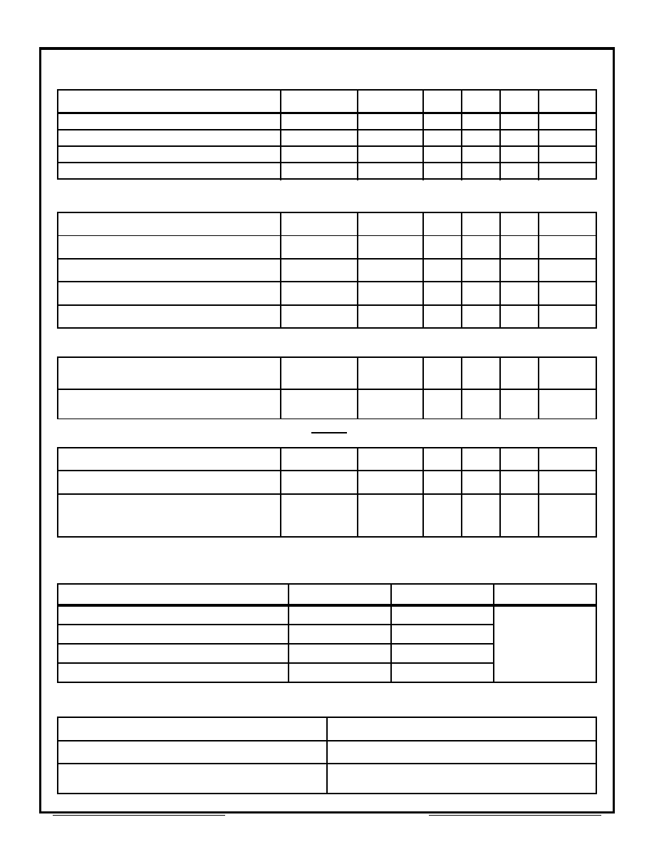
Electrical Characteristics Per Channel, Receiver Section
Parameter
Condition
Symbol
Min
Typ
Max
Unit
Differential Input Impedance
f = 1MHz
Z
In
20K
100K
Differential Input Voltage Range
V
IDR
40
V p-p
Input Common Mode Voltage Range
Note 1
V
ICR
10
V p-p
Common Mode Rejection Ratio
Note 1
CMRR
40
dB
Strobe Characteristics (Logic "O" inhibits output)
"0" Input Current
V
S
= 0.4 V
I
IL
-0.2
-0.4
mA
"1" Input Current
V
S
= 2.7V
I
IH
-1.0
+40
µA
"0" Input Voltage
V
IL
0.7
V
"1" Input Voltage
V
IH
2.0
V
Strobe Delay (turn-on or turn-off)
Note 1.
t
SD
150
nS
Threshold Characteristics (Sinewave input )
Internal Threshold Voltage (referred to the
bus) pins 6 and 11 grounded
100KHz-
1 MHz
V
TH
0.60
0.8
1.15
V
P-P
External threshold control ( pins 6&11 open,
resistors from pin 5 and 12 to ground)
Max R = 8K
R
TH
/V
TH
4000
Ohms /V
p-p
Output Characteristics, RX DATA and RX DATA
"1" State
I
OH
= -0.4 mA
V
OH
2.5
3.6
V
"0" State
I
OL
= 4 mA
V
OL
0.35
0.5
V
Delay, (average)from differential input zero
crossings to RX DATA and RX DATA output
50% points
Note 1
t
DRX
300
450
nS
Power Supply Currents Per Channel
(Power supplies set at +15V, -15V, +5V)
Duty Cycle
+V
CC
-V
EE
5V
Transmitter Standby or 1% Duty Cycle
60mA
75mA
35mA
25% duty cycle
Note 1
80mA
95mA
50% duty cycle
105mA
120mA
100% duty cycle Note 1
160mA
180mA
Recommended Power Supply Voltage Range
+V
+11.4 Volts to +15.75 Volts
-V
-11.4 Volts to -15.75 Volts
Logic
+4.5 Volts to + 5.5 Volts
Aeroflex Circuit Technology SCD4808 REV A 3/9/98 Plainview NY (516) 694-6700
5
NOTES
1. Characteristics guaranteed by design, not production tested.
2. Measured from 75kHz to 1MHz at point A-A' with transformer self impedance of 3K
minimum, power on or off
Figure 3 Transmitter (TX) Output Wave form Figure 4 Transmitter (TX) Output offset
Figure 5 Typical Transformer connection
6.5V P-P MIN
8.5V P-P MAX
90%
10%
t
r
*
t
f
*
* Rise and fall times measured at point A-A' in Fig 5
0 Volts
OUTPUT OFFSET
*
OUTPUT OFFSET
*
LAST BIT
2.5 µsec
*Offset measured at point A-A' in Fig 5
N1:N2
A
A'
B'
B
TX DATA OUT
TX DATA OUT
RX DATA IN
RX DATA IN
70
70
52.5
52.5
Ctr
tap
Transformer turns ratios:
N1:N2 = 1:1
N1:N3 = 1:0.71
Use Aeroflex 25T1553-1
N1:N3 for
stub
coupling
0 Volts
Magnified View
Figure 6 Power Dissipation vs. Duty Cycle
0 10 20 30 40 50 60 70 80 90 100
4.0
3.5
3.0
2.5
2.0
1.5
1.0
0.5
0
DUTY CYCLE, PERCENT
P
O
W
E
R
D
I
S
S
I
P
A
T
I
O
N
W
A
T
T
S
(TYPICAL)
(Per Channel)
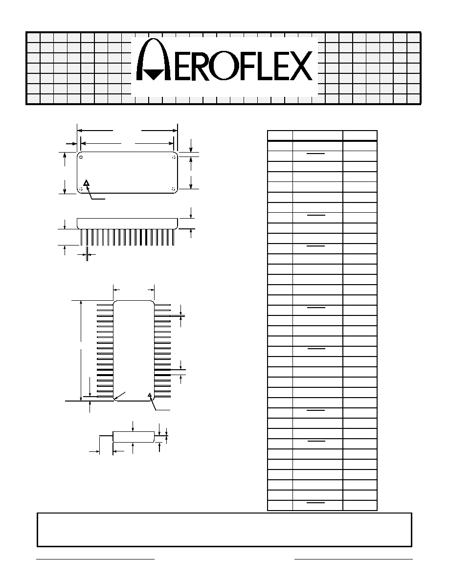
Configurations and Ordering Information
Model No. DESC No.
Receiver Data level
Case
ARX4808
TBA Normally High Plug In
ARX4808-2
TBA Normally High Flat Pack
ARX4868
TBA Normally Low Plug In
ARX4868-2
TBA Normally Low
Flat Pack
Aeroflex Circuit Technology
SCD4808 REV A 3/9/98 Plainview NY (516) 694-6700
6
Dual In Line
1.70
1.90 MAX
0.78
MAX
.097
36
19
18
Flat Package
0.600
0.085
0.24
MIN
0.018 DIA.
±0.002
0.10 Typ
0.015
±0.002
0.78 MAX
19
18
36
1.90 MAX
0.097
0.086 R
4 Places
0.40
MIN
2 SIDES
0.175 MAX
0.065
REF
0.010
±0.002
Notes
1. Dimensions shown are in inches
2. Pins are equally spaced at 0.100±0.002 tolerance,
non-cumulative, each row
Pin Numbers & Functions
Pin #
Function
Channel
1
TX DATA OUT
A
2
TX DATA OUT
A
3
GROUND
A
4
NC
5
RX DATA OUT
A
6
STROBE
A
7
GROUND
A
8
RX DATA OUT
A
9
CASE
10
TX DATA OUT
B
11
TX DATA OUT
B
12
GROUND
B
13
NC
14
RX DATA OUT
B
15
STROBE
B
16
GROUND
B
17
RX DATA OUT
B
18
NC
19
VCC
B
20
RX DATA IN
B
21
RX DATA IN
B
22
GROUND 3
B
23
VEE
B
24
+5V
B
25
INHIBIT
B
26
TX DATA IN
B
27
TX DATA IN
B
28
VCC
A
29
RX DATA IN
A
30
RX DATA IN
A
31
GROUND
A
32
VEE
A
33
+5 V
A
34
INHIBIT
A
35
TX DATA IN
A
36
TX DATA IN
A
Specifications subject to change without notice.
Pin 1 & ESD
Designator
Pin 1 & ESD
Designator
Aeroflex Circuit Technology
35 South Service Road
Plainview New York 11803
Telephone: (516) 694-6700
FAX: (516) 694-6715
Toll Free Inquiries: 1-(800) THE-1553
C I R C U I T T E C H N O L O G Y