 | –≠–ª–µ–∫—Ç—Ä–æ–Ω–Ω—ã–π –∫–æ–º–ø–æ–Ω–µ–Ω—Ç: CT2556-FP | –°–∫–∞—á–∞—Ç—å:  PDF PDF  ZIP ZIP |
eroflex Circuit T
echnology
≠ Data Bus Modules For The Future © SCDCT2553 REV B 8/6/99
Features
I
Second Source Compatible to the BUS-61553
I
Complete Integrated MUX Including:
∑
Low Power Dual Transceiver
∑
BC/RTU/MT Protocol
∑
8K x 16 Shared Ram
∑
Interrupt Logic
I
Compatible with MIL-STD- 1750 and other Standard CPUs
I
DIP or Flatpack Hybrid
I
Minimizes CPU Overhead
I
Provides Memory Mapped 1553 Interface
I
On-Line & Off-Line Self-Test
I
PCs Development Tools Available
I
SEAFAC Tested
I
MIL-PRF-38534 compliant circuits available
I
DESC SMD #5962≠88692 Pending
I
Packaging ≠ Hermetic Metal
∑
78 Pin, 2.1" x 1.87" x .25" Plug-In type package
∑
82 Lead, 2.2" x 1.61" x .18" Flat package
General Description
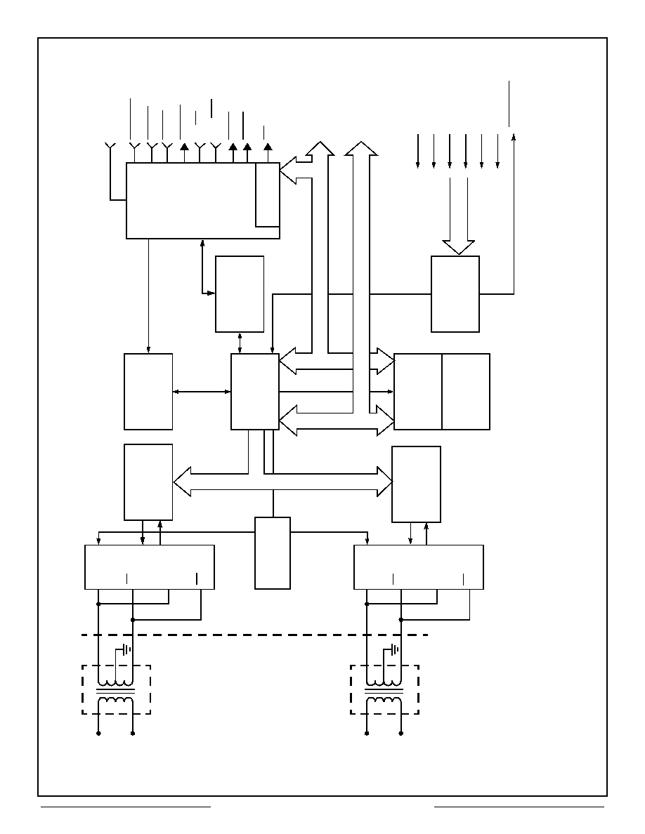
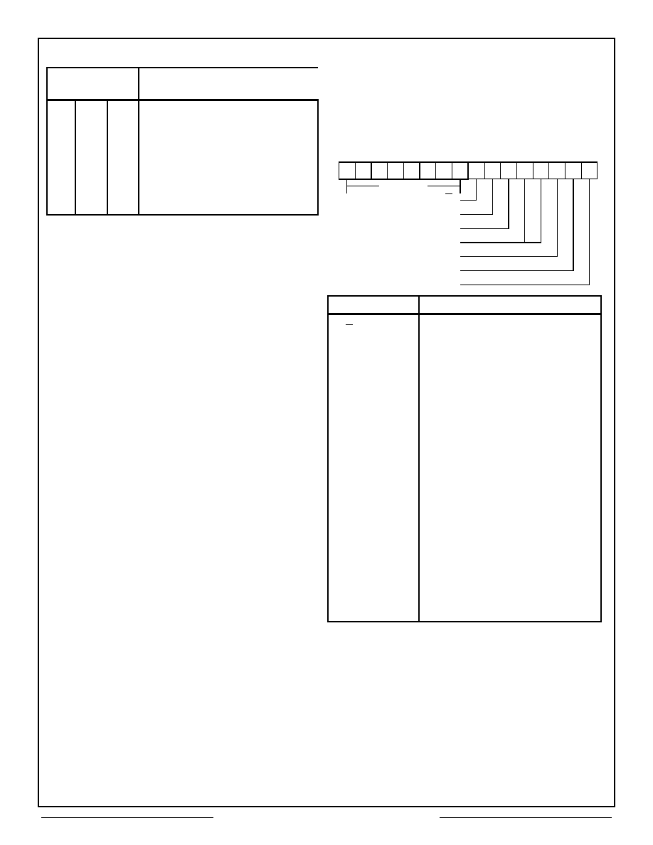
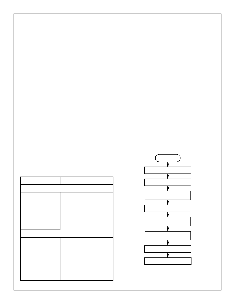
Aeroflex's CT2553 Advanced Integrated Mux (AIM) Hybrid is a complete MIL-STD-1553 Bus
Controller (BC), Remote Terminal Unit (RTU), and Bus Monitor (MT) device. Packaged in a single
78 pin DIP package, the CT2553 contains dual low-power transceivers, complete BC/RTU/MT
protocol logic, a MIL-STD-1553-to-host interface unit and an 8K x 16 RAM.
Using an industry standard dual transceiver and standard status and control signals, the CT2553
simplifies system integration at both the MIL-STD-1553 and host processor interface levels.
All 1553 operations are controlled through the CPU access to the shared 8K x 16 RAM. To ensure
maximum design flexibility, memory control lines are provided for attaching external RAM to the
CT2553 Address and Data Buses and for disabling internal memory; the total combined memory
space can be expanded to 64K x16. All 1553 transfers are entirely memory-mapped; thus the CPU
interface requires minimal hardware and/or software support.
The CT2553 operates over the full military -55∞C to +125∞C temperature range. Available screened
to MIL-STD883, the CT2553 is ideal for demanding military and industrial microprocessor to 1553
interface applications. See "Ordering Information" (last sheet) for CT2554, CT2555 & CT2556.
CT2553 / 2554 / 2555 / 2556
FOR MIL-STD-1553
F
I
E
I
D
C
E
R T
A
E
R
O
F
L E
X L A
B
S
I
N
C
.
ISO
9001
CIRCUIT TECHNOLOGY
www.aeroflex.com
Advanced Integrated MUX (AIM) Hybrid
Aeroflex Circuit Technology
2
SCDCT2553 REV B 8/6/99 Plainview NY (516) 694-6700
F
i
g
u
r
e
1
≠
C
T
2
5
5
3
B
l
o
c
k
D
i
a
g
r
a
m
R
T
A
D
R
2
R
T
A
D
R
0
R
T
A
D
R
4
R
T
A
D
R
3
R
T
A
D
R
1
R
T
A
D
R
P
T
R
A
N
S
C
E
I
V
E
R
B
1
2
3
4
8
D
A
T
A
B
U
S
A
1
2
3
4
8
T
R
A
N
S
F
O
R
M
E
R
B
D
A
T
A
B
U
S
B
T
R
A
N
S
C
E
I
V
E
R
A
R
T
A
D
D
R
R
T
P
A
R
E
R
R
I
N
T
E
X
T
L
D
E
X
T
E
N
M
E
M
/
R
E
G
R
D
/
W
R
R
E
A
D
Y
D
S
T
R
B
D
S
E
L
E
C
T
M
S
T
R
C
L
R
C
L
O
C
K
I
N
Q
1
5
5
3
-
2
Q
1
5
5
3
-
2
T
R
A
N
S
F
O
R
M
E
R
A
C
H
A
N
N
E
L
A
D
E
C
O
D
E
R
E
N
C
O
D
E
R
/
M
E
M
O
R
Y
T
I
M
I
N
G
C
O
N
T
E
N
T
I
O
N
R
E
S
O
L
V
E
R
C
H
A
N
N
E
L
B
D
E
C
O
D
E
R
E
N
C
O
D
E
R
/
R
X
R
X
T
X
T
X
I
N
H
R
X
R
X
T
X
T
X
I
N
H
T
I
M
E
O
U
T
7
6
8
µ
s
8
K
X
1
6
S
H
A
R
E
D
R
A
M
R
A
M
P
A
R
I
T
Y
C
H
E
C
K
E
R
C
P
U
T
I
M
I
N
G
I
N
T
E
R
R
U
P
T
G
E
N
E
R
A
T
O
R
P
R
O
T
O
C
O
L
C
O
N
T
R
O
L
L
E
R
A
1
5
-
A
0
0
D
1
5
-
D
0
0
N
o
t
e
:
T
h
e
W
a
t
c
h
-
D
o
g
T
i
m
e
O
u
t
(
7
6
8
µ
s
T
Y
P
.
)
i
s
b
u
i
l
t
i
n
.

Aeroflex Circuit Technology
3
SCDCT2553 REV B 8/6/99 Plainview NY (516) 694-6700
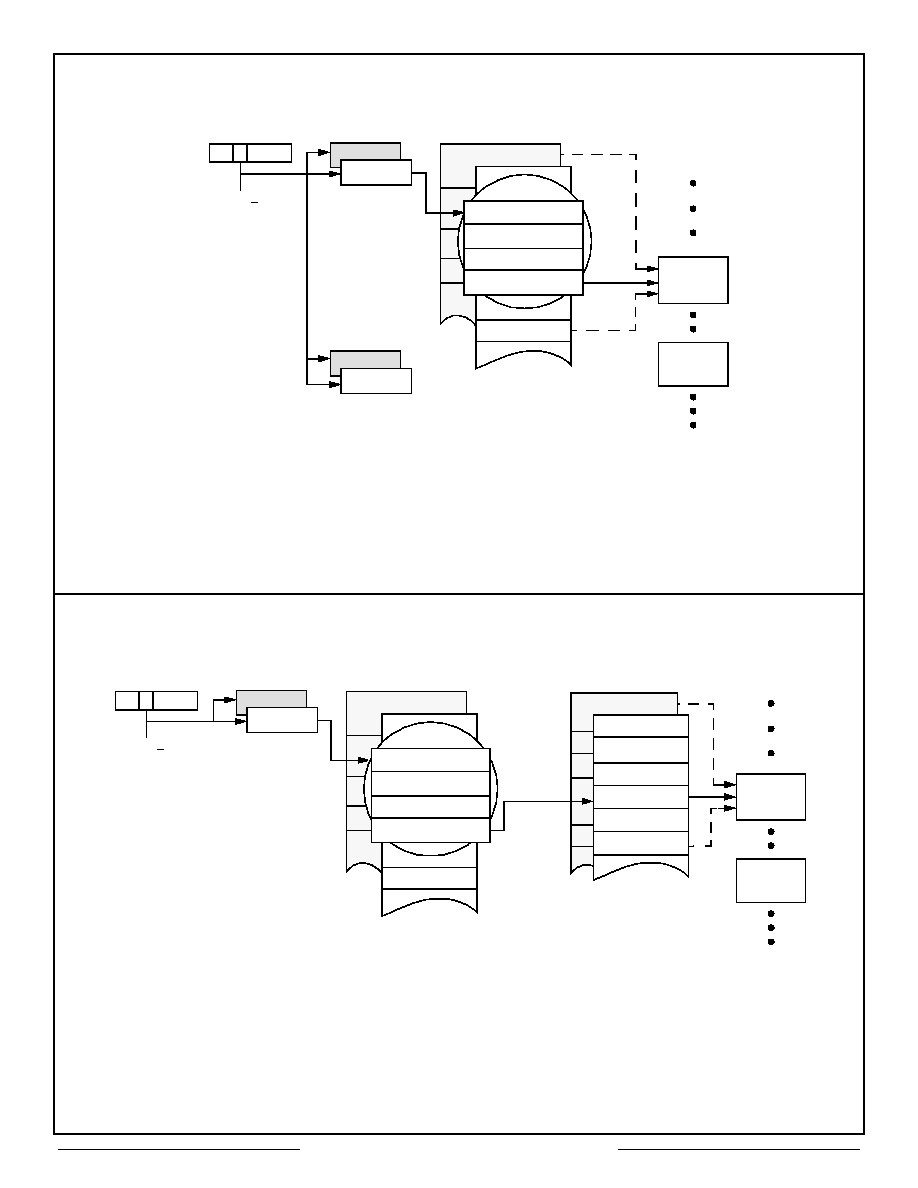
GENERAL
The CT2553 is a complete MIL-STD-1553 bus
interface unit containing dual low-power
transceivers; Bus Controller (BC), Remote
Terminal (RTU), and Bus Monitor (MT) protocol
logic; 8K x 16-bit pseudo dual port RAM; and
memory management arbitration control circuitry.
The host processor interface consists of standard
control and interrupt signals, memory expansion
capability and non-multiplexed address and data
buses.
Control of the CT2553 is accomplished entirely
through the use of three internal registers and the
shared RAM. Transfers to and from the CT2553
are executed on a word-by-word basis ensuring
minimal wait time if contention occurs.
The specific mods of operation (1553
BC/RTU/MT) is software programmable. Memory
is configured into unique control and data block
areas based on the 1553 mode of operation.
External registers are also supported by the
CT2553 for manipulation of user data. In addition,
the CT2553 provides dynamic, online and
software initiated self-test capabilities.
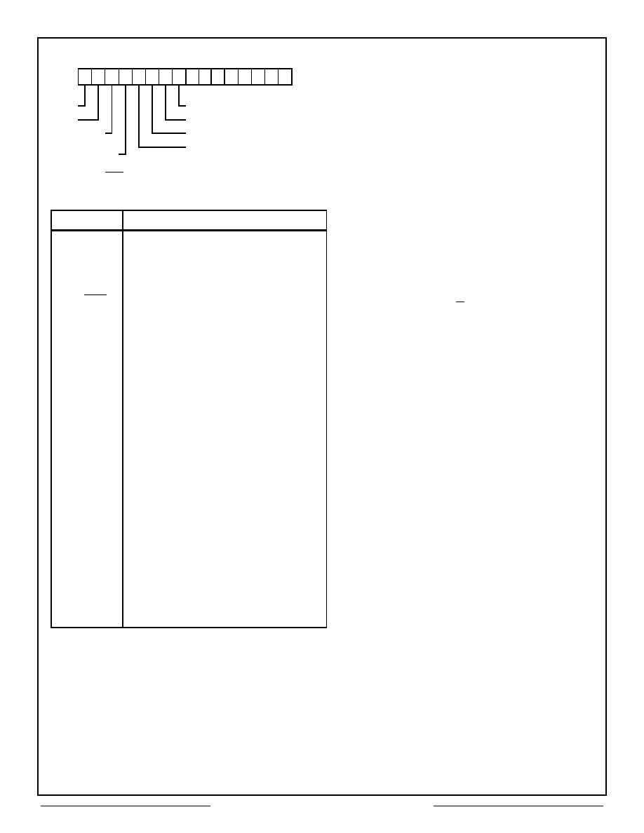
Values at nominal Power Supply Voltages unless otherwise specified
PARAMETER
VALUE
UNITS
Receiver
Differential Input Voltage
40 max
Vp-p
Differential Input
Impedance
7 min
K
CMRR
40 min
db
Transmitter (Direct Coupled)
Differential Output Voltage
6.0 min, 9.0 max
Vp-p
Output Rise and Fall Times
100 min, 300 max
nsec
Output Offset Voltage
±90 max
mV
Logic*
V
IH
2.2 min
V
V
IL
0.8 max
V
Clock
16
MHZ
Power Supplies
+5V (Logic)
+5±5%
V
-15VA (Channel A Transceiver)
-15±10%
V
-15VB (Channel B Transceiver)
-15±10%
V
+5VA (Channel A)
+5±5%
V
+5VB (Channel B)
+5±5%
V
Current Drain* (Total Package)
(TYP)/max
+5V (Idle)
(85)/170
mA
-15V (Idle)
(45)/80
mA
+5V (25% Duty Cycle)
(85)/170
mA
-15V (25% Duty Cycle)
(80)/130
mA
Temperature Range
Operating (Case)
-
55 to +125
∞C
Storage
-
65 to +150
∞C
Physical Characteristics
Size
78 pin DDIP
2.1 x 1.87 x 0.25
(53 x 47.5 x 6.4)
in
(mm)
82 pin flatpack
2.19 x 1.6 x 0.175
(55.6 x 40.6 x 4.34)
in
(mm)
* See Table 7 for pin loading characteristics.
Table 1 ≠ CT2553 Specifications

Aeroflex Circuit Technology
4
SCDCT2553 REV B 8/6/99 Plainview NY (516) 694-6700
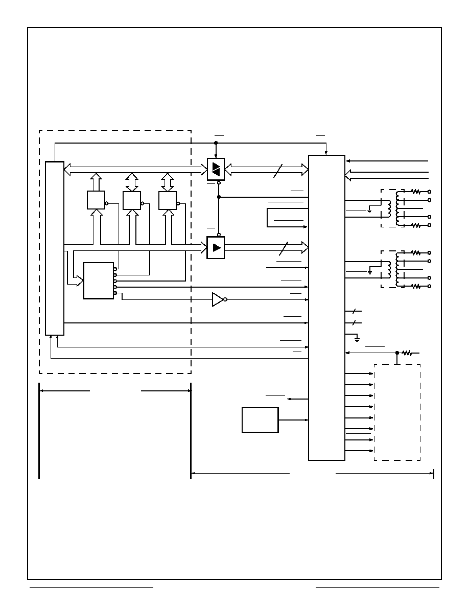
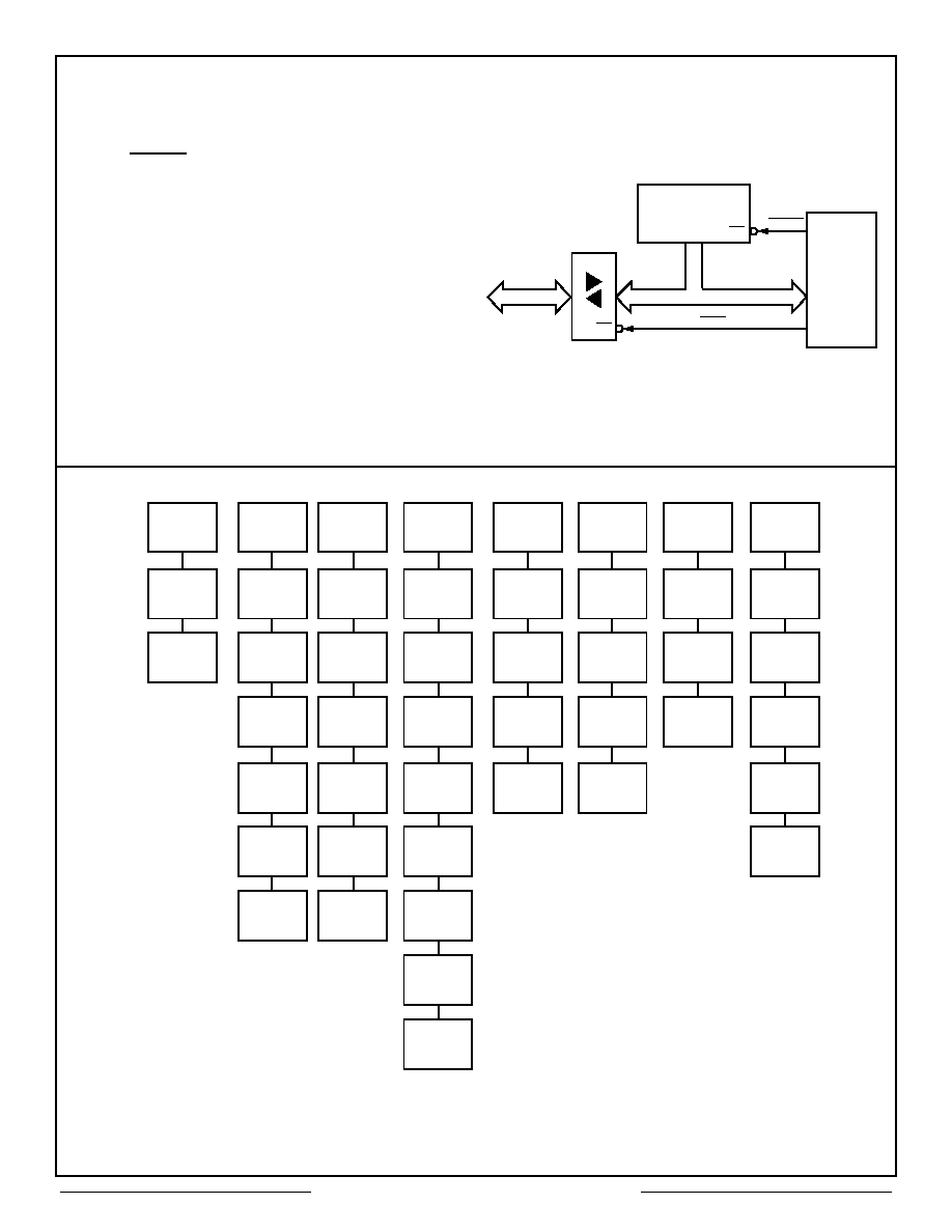
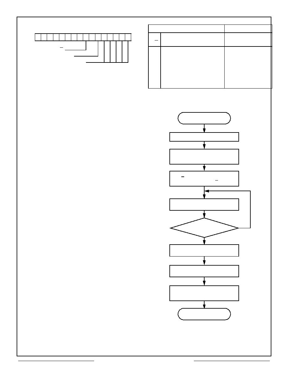
INTERFACING
The CT2553 is compatible with most common
microprocessors including, but not limited to, the
Motorola 680 x 0, the Intel 808x, Zilog Z800x and
MIL-STD-1750 processors.
Interfacing the CT2553 to the MIL-STD-1553
Data Bus requires two Q1553-2 pulse
transformers and an external 16 MHz clock (See
Figure 2). Tri-state buffers are used to isolate the
CPU's data and address lines.
External RAM can be used instead of or in
conjunction with the CT2553's internal 8K x 16
bits. The external RAM used by the CT2553 can
be any standard static memory with an access
time of < 55ns. The external RAM can be
expanded to 64K x 16.
Two control signals, MEMENA-IN (pin 69) and
MEMENMA-OUT (pin 31) are provided in
addition to the standard memory I/O signals for
internal/external memory access control (See
Figures 3-5. MEMEN-OUT and MEMEN-IN
should be tied together for Internal Memory Only
configuration. Memory CS signals can be
generated for configurations using external
memory.
MEMORY MANAGEMENT
Memory can be configured to support two AREAs
(A and B), each with an independent sequential
stack and pointers for manipulating 1553
message and control data. The CPU can access
the shared RAM while 1553 message transfers
are taking place. Arbitration of the RAM is
automatically implemented in a manner
transparent to the subsystem (See Figures
28-31). Variable Length DATA BLOCKS are also
stored in the shared RAM and can be addressed
by setting pointers residing in Area A, Area B or
both.
For BC/RTU operation, each area contains a
Descriptor Stack and Stack Pointer (See Figures
6 and 7). BC operation further maintains a
Message Count for each area (number of 1553
messages per frame). RTU operation maintains a
data block address Look-Up Table for each area.
MT operation utilizes a single Stack Pointer to
indicate the starting address for storage of
received words and associated identification
Words.
CURRENT AREA ASSIGNMENT/SWAPPING.
Current area status (currently available to the
1553 terminal) is Software programmable by the
host; the unassigned area automatically assumes
non-current area status. Both areas are always
addressable by the host. Swapping of the Current
Area can be done following message transfers for
user operations such as exception handling or
multiple buffering of 1553 data.
The host selects the Current Area by writing to
the CT2553's Configuration Register with bit 13
set to the appropriate logic level (0 for area A or 1
for area B). Internal circuitry ensures that the
swapping of Current Area Status does not occur
during an ongoing message transfer (See
Configuration Register).
DESCRIPTOR STACK (BC/RTU). The
DESCRIPTOR STACK (DS) is divided into 64
entries. Each stack entry contains four words
which refer to one 1553 message. The Block
Status Word (BSW) indicates the physical bus on
which the message was received (RTU mode),
reports whether or not an error was detected
during message transfer and indicates message
completion (See Figure 8).
The user-supplied Time Tag word is loaded at the
start of a message transfer and is updated at the
end of the transfer (See Time Tagging).
Aeroflex Circuit Technology
5
SCDCT2553 REV B 8/6/99 Plainview NY (516) 694-6700
TX/RX-A
4
5
6
7
8
3
2
1
+
≠
TX/RX-A
BUS-25679
TX/RX-B
4
5
6
7
8
3
2
1
+
≠
TX/RX-B
BUS-25679
RTADDRESS
RTADP
1553 INTERFACE
+5V
-15V
+5V
MEMOE
HOST PROCESSOR
INT
STRBD
READYD
(54LS04)
MEM/REG
MSTRCLR
POR
SELECT
(SEE NOTE 2)
A0 - A12
ADDRESS
13
MEMENA-IN
MEMENA-OUT
(SEE NOTE 1)
(54LS244)
(OE)
ADDRESS
DECODER
(OE)
(DIR)
(54LS245)
DATA
D0 - D15
IOEN
16
ILLCMD
SA/MC-0
SA/MC-1
SA/MC-2
SA/MC-3
SA/MC-4
T/R
BCSTRCV
LMC
RD/WR
RD/WR
16MHz
CLOCK
20
59
69
31
73
71
74
33
34
75
72
12
36
30
32
17
XX
57
53
54
52
15
13
CT2553
ILLEGALIZATION
PROM
(OPTIONAL)
40
78
51
3
2
CPU
ROM
RAM
I/O
A0 - A12
Figure 2 ≠ CT2553 Example Interconnection
Aeroflex Circuit Technology
6
SCDCT2553 REV B 8/6/99 Plainview NY (516) 694-6700
CT2553
69
31
MEMENA OUT
MEMENA IN
ADDRESS BUS
CPU
MEMENA IN
MEMENA OUT
CS
CPU
16
ADDRESS BUS
10K
+5V
64K x 16
STATIC RAM
31
69
CT2553
MEMENA OUT
ADDRESS BUS
CPU
13
MEMENA IN
56 x 16K STATIC RAM MAX
8K
x
16
8K
x
16
8K
x
16
8K
x
16
8K
x
16
8K
x
16
8K
x
16
ADDRESS
DECODER
E
A
B
C
1
2
3
4
5
6
7
0
A13
A14
A15
31
69
CT2553
Figure 5 ≠ Configuration Using Both Internal and External Memory
Figure 3 ≠ Internal Memory Only
Figure 4 ≠ External Memory Only
ADDRESS
DECODER
E
Aeroflex Circuit Technology
7
SCDCT2553 REV B 8/6/99 Plainview NY (516) 694-6700
Figure 6 ≠ Use of Descriptor Stack ≠ BC Mode
* Note:
STACK POINTERS and MESSAGE COUNTERS are switched via the
CONFIGURATION REGISTER under external CPU control.
** Note:
DESCRIPTOR STACKS and DATA BLOCKS have 256 word boundries which
should be observed.
Figure 7 ≠ Use of Descriptor Stack ≠ RTU Mode
DESCRIPTOR
**
STACKS
STACK
POINTERS
CONFIGURATION
REGISTER
CURRENT
AREA B/A
DATA
**
BLOCKS
DATA BLOCK
DATA BLOCK
0
13
15
BLOCK STATUS WORD
RESERVED
TIME TAG WORD
MESSAGE
BLOCK ADDR
DESCRIPTOR
**
STACKS
STACK
POINTERS
CONFIGURATION
REGISTER
CURRENT
AREA B/A
DATA
**
BLOCKS
DATA BLOCK
DATA BLOCK
0
13
15
LOOK-UP TABLE
(DATA BLOCK ADDR)
LOOK-UP
TABLE ADDR
BLOCK STATUS WORD
RESERVED
TIME TAG WORD
RECEIVED COMMAND
WORD
*
*
MESSAGE
COUNTER
*
*
* Note:
STACK POINTERS and LOOK-UP TABLE are switched via the
CONFIGURATION REGISTER under external CPU control.
** Note:
DESCRIPTOR STACKS and DATA BLOCKS have 256 word boundries which
should be observed.
Aeroflex Circuit Technology
8
SCDCT2553 REV B 8/6/99 Plainview NY (516) 694-6700
The contents of the fourth word of the stack entry
depends upon the 1553 operating mode selected.
In BC mode, It contains the address of the
associated 1553 message (Data Block). In RTU
mode, it contains the complete (received) 1553
Command Word.
STACK POINTER. A STACK POINTER (SP) is
maintained at a specified location in shared RAM
for each Descriptor Stack (SP-A: 0100H; SP-B:
0104H). Each Stack Pointer must be initialized by
the CPU to point to the Descriptor Stack Entry to
be used for the first MIL-STD-1553 transmission.
The current area SP is automatically incremented
by four following each message transfer thereby
always pointing to the next Block Status Word.
Note: The Stack Pointer is maintained internally using an
8-BIT REGISTER for the HIGH BYTE and an 8-BIT
COUNTER for the LOW BYTE. The high byte remains
constant (user value) while the low byte will wrap around
from FF(H) to 00(H). For example: a current Stack Pointer
value of 00 FF(H) will increment to 00 00(H) and not
01 00 (H).
LOOK-UP TABLE (RTU). A data block address
Look-Up Table is used to indicate the data blocks
to be used for individual commands. Look-Up is
based upon the T/R (transmit/receive) and
Subaddress bits of the received 1553 Command
Word. See RTU Operation for detailed operation;
two tables are provided for double buffering in the
RTU mode.
MULTIPLE BUFFERING (BC/RTU). Unused
areas of shared RAM can be used to store
additional stacks, tables, data blocks and/or user
(non 1553-related) data. In this way, multiple data
blocks (RTU) or messages (BC) can be stored for
later use: simply update respective pointers and
initiate the appropriate start conditions. (BC mode
requires SP, message block address and message
count updating while in RTU mode, the SP and
Look-Up Table entry must be updated).
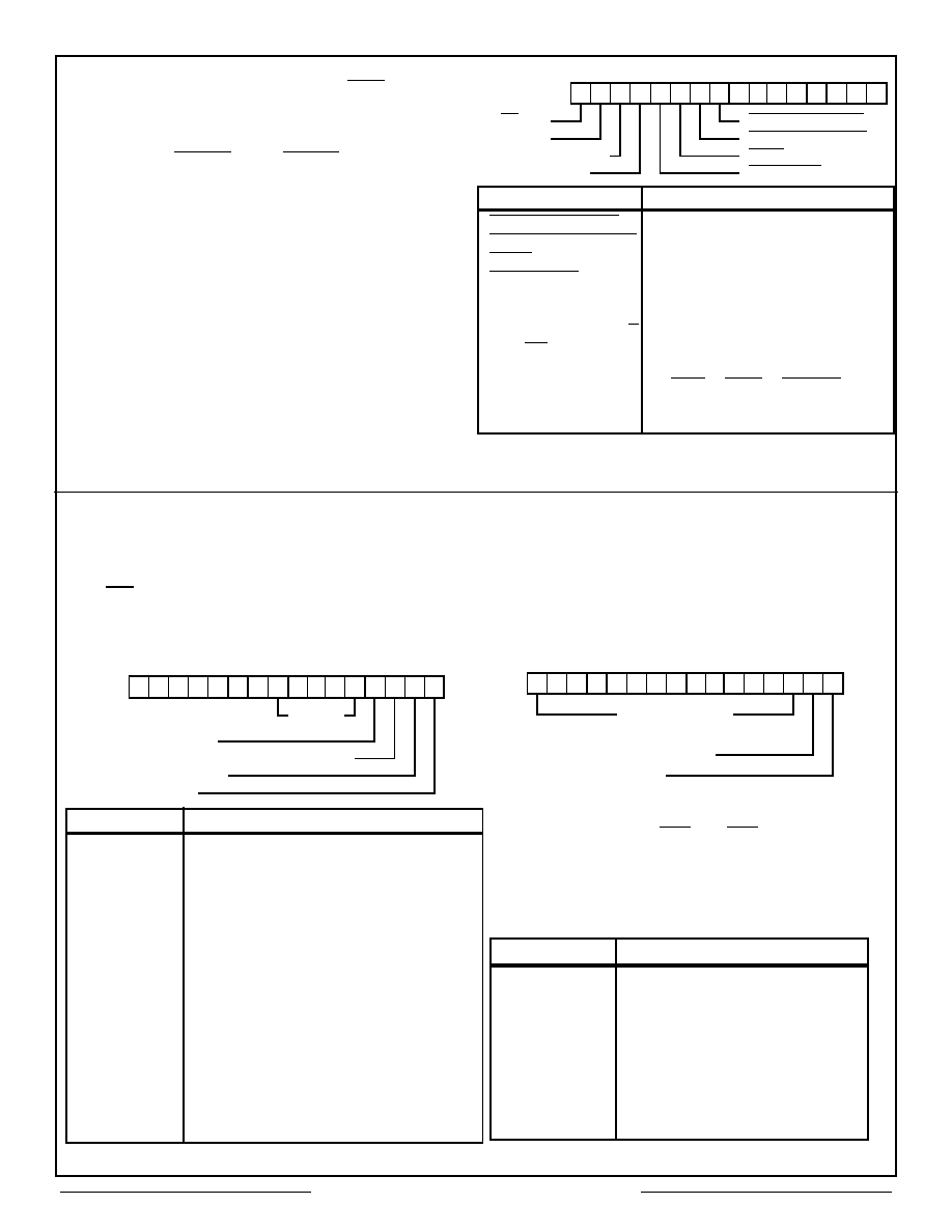
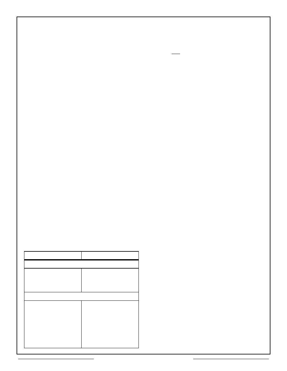
CT2553 REGISTERS
The CT2553 is controlled through the use of three
internal registers: Interrupt Mask Register,
Configuration Register and a Start/Reset Register.
In addition, the CT2553 can access up to four
external, user supplied registers (See Table 2).
Possible external register applications include:
CPU Time Tag storage and RTU Address
assignment (See Figures 9 and 10).
15
8 7
0
1 1 1 1 1 1 1 1
EOM
LOOP TEST FAIL
SOM
RESPONSE TIME OUT (BC ONLY)
CHB/CHA
(RTU ONLY)
FORMAT ERROR
STATUS SET (BC ONLY)
ERROR FLAG
Note: In BC operation, the CT2553 always writes the BSW to RAM with
Bit-13. CHB/CHA toggles as per the message control word setting.
BIT NAME
DEFINITION
EOM
Set at the completion of a message
transfer regardless of whether any errors
were detected.
SOM
Set at the beginning of a message transfer
and Reset upon completion of the transfer.
CHB/CHA
Set in RTU mode to indicate whether the
message was received on 1553 bus A or
bus B. Toggles to indicate channel, in BC
mode.
ERROR
FLAG
Indicates that an error was detected within
the message transfer. The specific error
condition(s) are identified in bits 8-11.
STATUS SET Set in BC mode to indicate that a status
flag bit was set within the received RTU
Status Word or that the RTU address did
not match the associated Command. Set
in BC mode when the message error bit is
set within the received RTU Status Word.
FORMAT
ERROR
Also set in RTU mode (RT-RT transfer;
CT2553 is acting as the receiving RT)
when the transmitting RTU Status Word
contains an incorrect address. Also, set in
BC or RTU mode if the message violates
MIL-STD-1553 (parity, Manchester, sync
bit count, non-contiguous data or word
count errors).
RESPONSE
TIMEOUT
Set in BC mode if the addressed RTU did
not respond within 14µs. Also set when
acting as a receiving RT (RT-RT transfer) if
the transmitting RT does not respond in
the specified 1553 response time.
LOOP
TEST FAIL
Set when the CT2553 does not pass the
Loop Test. See Self Test paragraph.
Figure 8 ≠ Descriptor Stack - Block Status
Word
Aeroflex Circuit Technology
9
SCDCT2553 REV B 8/6/99 Plainview NY (516) 694-6700
E
B
A
E
B
A
DECODER
ADDRESS
EXTEN
EXTLD
WRITE
READ
A00
A00
A01
A01
{
{
EXTLD
CPU
DATA BUS
D15 - D00
IOENBL
CT2553
RT ADDR
RTADP
REGISTER
1
5
16
6
OE
Figure 9 ≠ Use of External Registers
Figure 10 ≠ Example Configuration Using External Registers
Note:
A02 of the CT2553 must be set to logic 1 to operate with external registers.
Aeroflex Circuit Technology
10
SCDCT2553 REV B 8/6/99 Plainview NY (516) 694-6700
CPU TO REGISTER OPERATIONS. The CPU
selects a register by asserting MEM/REG low and
A2 to a logic 0 (for internal registers) or logic 1 (for
external registers) with A0 and A1 indicating the
appropriate register address (See Figures 28-32).
The signals EXTEN and EXTLD are used to
access the external registers.
CONFIGURATION REGISTER. The Configuration
Register is a 16-bit read/write register used to
define the 1553 operating mode (BC, RTU, or MT);
define selectable 1553 Status Word bits (RTU
only); select stop-on-error option; and support the
double buffering scheme (See Figure 11).
15
8 7
0
1 1 1 1 1 1 1 1
RTU/BC
SUBSYSTEM FLAG
MT
SERVICE REQUEST
CURRENT AREA B/A
BUSY
STOP ON ERROR
DB ACCEPT
BIT NAME
DEFINITION
SUBYSTEM FLAG
Sets/resets 1553 Status Word flag.
SERVICE REQUEST
Sets/resets 1553 Status Word flag.
BUSY
Sets/resets 1553 Status Word flag.
DB ACCEPT
Sets/resets 1553 Status Word flag.
STOP ON ERROR
BC will halt message transfer after
completing current EOM cycle.
CURRENT AREA B/A Selects Current Area Pointers.
RTU/BC
RTU or BC-MT Operation Select.
Note: A logic 0 causes the corresponding bit within the RTU's status
word to be set to a logic 1.
Figure 11 ≠ Configuration Register
BIT15
BIT 14
Operation
0
0
BC
0
1
MT
1
0
RTU
1
1
Illegal
INTERRUPT MASK REGISTER (BC/RTU). This
register is a 16-bit read/write register used to
enable/mask interrupt conditions. If an interrupt
condition occurs and the corresponding Interrupt
Register bit has been enabled (set to logic 1) pin
72, INT will be pulsed low during the respective
End of Message (EOM) cycle (See Figure 12). Not
Used bit locations can optionally be used for
storing user flags.
START/RESET REGISTER. This write-only
register is used to reset the CT2553 and to start
the BC and MT operations, as illustrated in
Figure 13.
15
9 8 7
4 3 2 1 0
1 1 1 1 1 1 1
NOT
USED
BC EOM
FORMAT ERROR/STATUS SET
NOT USED
EOM
INTERRUPT
DEFINITION
EOM
End of message. Set by CT2553 in BC or
RTU mode following each 1553 transfer
(regardless of validity).
FORMAT
ERROR/
STATUS SET
Set if one of the following occurs:.
Loop Test Failure: Received word does
not match last word transmitted.
Message Error: Received message
contained a violation of any of the 1553
message validation criteria (parity, sync,
manchester encoding, bit/word count, etc.)
Time-Out: Expected transmission was
not received during the allotted time.
Status Set: Received Status Word
contained status bit(s) set or address error.
BC EOM
Bus Controller End of Message. Set by the
CT2553 following transmission of all
messages within the current Message Block
(Current area message count = FFFF).
Figure 12 ≠ Interrupt Mask Register
15
9 8 7
4 3 2 1 0
NOT USED
CONTROLLER START
RESET
BIT NAME
DEFINITION
CONTROLLER
START
Issued by the CPU to start
message block transmission (BC
Operation) or to begin reception of
1553 messages (MT Operation).
RESET
Issued by the CPU to place the
CT2553 in the power-on condition;
(1) aborts 1553 transfers currently
in progress, and (2) resets
Configuration and Interrupt Mask
Register bits (logic 0).
Figure 13 ≠ Start/Reset Register
BIT 1
BIT 0
START
1
0
RESET
0
1
Aeroflex Circuit Technology
11
SCDCT2553 REV B 8/6/99 Plainview NY (516) 694-6700
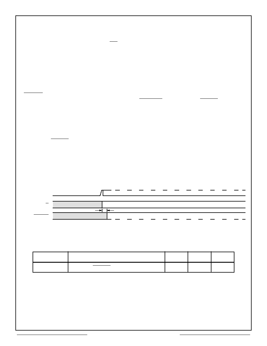
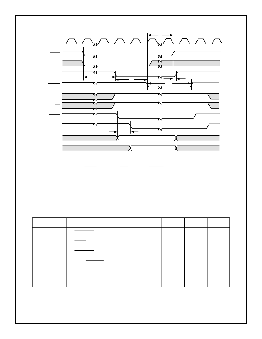
CONTENTION HANDLING
The CT2553 arbitrates shared RAM (and control
register) accesses between the host CPU and the
internal 1553 protocol logic.
If the host attempts to access the RAM while an
internal 1553 memory cycle is in progress, the
CT1553 will delay the CPU's memory cycle by
inserting wait states via the READYD control
signal until the cycle has been completed. The
maximum delay is 1.8µs.
If the internal 1553 protocol logic attempts to
access the RAM while the host CPU has control of
the memory, the internal 1553 logic will wait until
the host CPU cycle has been completed. To
ensure the integrity of 1553 data transfers, the
host CPU must complete its memory cycle within
1.5µs (See Figures 28-32).
SELF TEST
The CT2553 has two self-test modes: the
automatic, continuous On-Line test and the
software-initiated Off-Line test. In both tests the
Loop Test Fail bit within the Block Status Word will
be set to a logic 1 if a failure is detected.
ON-LINE TEST. The On-Line test occurs in BC
and RTU modes during transmission of each
message onto the 1553 bus. This test wraps
around the last word transmitted, exercising the
1553 protocol logic through the 1553 transceivers.
While operating as a BC, the last word transmitted
is received, decoded, and written back into
memory location immediately following the last
word within the message block. The host CPU can
read and compare this Loop Back Word with the
last word of the message Data Block; these two
words should be identical. This insures data
integrity between the CPU and the CT2553.
While in the RTU mode, the internal 1553 Status
Word will be updated to reflect the result of the self
test. The Status Word's Terminal Flag bit will be
set to a logic 1 if a fault was indicated by the
wrap-around, self-test.
OFF-LINE TEST. The software-initiated Off-Line
test can be executed only when the CT2553 is
configured as a BC. Set the Wrap-Around Test bit
within the BC Control Word to a logic 1 and initiate
any standard message transfer. This inhibits the
1553 transceivers and initiates the standard
wrap-around test (i.e., internal 1553 encoder
output is fed back into the decoder - the word is
then written into memory). See BC Operation and
Figure 14, BC Control Word for more details.
RESET
The CT2553 can be reset by pulsing the
MSTRCLR (pin 71) low or by writing to the
Start/Reset register. After a reset condition has
occurred, the Configuration, Interrupt, and
(internal) Block Status word register outputs are
forced to a logic 0.
Table 2 ≠ CT2553 Register Address Definition
Address Bits
Definition
A2
A1
A0
0
0
0
R/W
Interrupt Mask Register
0
0
1
R/W
Configuration Register
0
1
0
≠
Not Used
0
1
1
W
Start/Reset Register
1
0
0
R/W
* External Register
1
0
1
R/W
* External Register
1
1
0
R/W
* External Register
1
1
1
R/W
* External Register
* Note: R/W (read/write) capability is dependent on the user's
decoding implementation (See Figure 9).
15
8
7
6
5
4
3
2
1
0
NOT USED
BUS CHANNEL A/B
OFF-LINE SELF TEST
MASK BROADCAST
NOT USED
MODE CODE
BROADCAST
RT-RT
BIT NAME
DEFINITION
BUS CHANNEL
A/B
Determines whether message will be
transmitted on 1553 Bus A or Bus B.
Logic 1 = A, logic 0 = B.
INITIATE
OFF-LINE SELF
TEST
Logic 1 performs internal off-line
transmit/receive test. The last word
of the message is looped back
through the decoder and placed in
RAM. See Self Test paragraph.
MASK
BROADCAST (1)
When logic 1, prevents Broadcast
RCVD bit of the 1553 Status Word
response from signalling a status
error as a result of a Broadcast
command. (A FORMAT error will be
generated if the BROADCAST bit is
not set on the RTU's Status Word.)
MODE CODE
When logic 1, the message is treated
as a Mode Code. (The Command
Word - Word Count field indicates
Mode Code type.)
BROADCAST
When logic 1, indicates that the
message is a Broadcast Command.
(No Status Word is expected.)
RT-RT
When logic 1, the message is treated
as an RT-RT transfer. (The next two
words are Command Words.) Both
Status Word responses are
validated.
Note:
1. MASK BROADCAST XOR BROADCAST BIT in Status Word =
STATUS SET ERROR.
2. When the BC expects the BROADCAST bit set in the Status Word,
a logic 1 will mask the Status Interrupt Error flag.
Figure 14 ≠ BC CONTROL WORD
Aeroflex Circuit Technology
12
SCDCT2553 REV B 8/6/99 Plainview NY (516) 694-6700
CONTROL
WORD
CONTROL
WORD
CONTROL
WORD
CONTROL
WORD
CONTROL
WORD
CONTROL
WORD
RECEIVE
COMMAND
TRANSMIT
COMMAND
RECEIVE
COMMAND
MODE
COMMAND
TRANSMIT
COMMAND
CONTROL
WORD
MODE
COMMAND
MODE
COMMAND
BROADCAST
COMMAND
DATA WORD
1
STATUS
WORD
STATUS
WORD
STATUS
WORD
DATA WORD
1
DATA WORD
2
DATA WORD
LAST
DATA WORD
1
DATA WORD
2
DATA WORD
LAST
STATUS
RECEIVE
DATA WORD
1 RECEIVED
DATA WORD
2 RECEIVED
DATA WORD
DATA WORD
RECEIVED
STATUS
RECEIVED
STATUS
WORD 1
FROM XMTR
STATUS
WORD 2
RECEIVER
FROM
TERMINAL TO
TERMINAL
LAST DATA
WORD
RECEIVED
DATA WORD
LOOPED
BACK
REMOTE
REMOTE
DATA BLOCK
COMMAND
BACK
BROADCAST
LOOPED
COMMAND
BACK
MODE
LOOPED
DATA WORD
BACK
LOOPED
LAST
BACK
DATA WORD
LOOPED
TRANSMIT
DATA BLOCK
RECEIVE
DATA BLOCK
WITH DATA
DATA BLOCK
MODE CODE
TRANSMIT
FORMAT
WITH DATA
DATA BLOCK
MODE CODE
RECEIVE
FORMAT
MODE CODE
WITHOUT
DATA
BROADCAST
COMMAND
WITH DATA
BROADCAST
COMMAND
(NO DATA)
BROADCAST
COMMAND
(NO DATA)
Figure 16 ≠ BC Message Formats
COMMAND
BACK
MODE
LOOPED
COMMAND
BACK
TRANSMIT
LOOPED
COMMAND
BACK
TRANSMIT
LOOPED
CONTROL
WORD
DATA WORD
2
DATA
WORD LAST
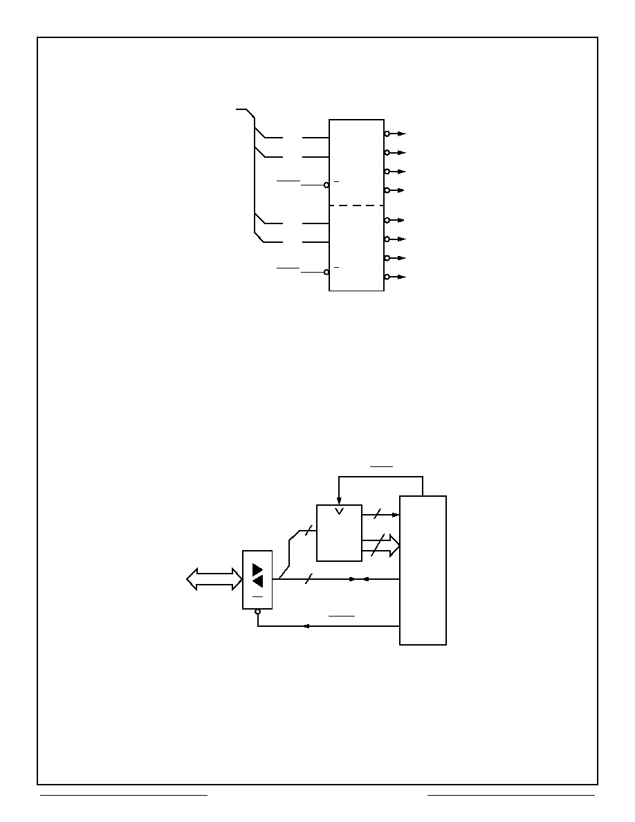
TIME TAGGING (OPTIONAL)
The CT2553 will automatically access an external,
3-state device (i.e., counter) at the start and end of
each message in BC or RTU modes. The CT2553
output, TAGEN (pin 76), enables the device's output
onto the common, 16-bit data highway while
executing a memory-write cycle. The device's value
is written into the second location of the Descriptor
Stack Entry. If a counter is used its clock, enable,
and reset control lines are connected per system
requirement (See Figure 15). If no external device is
attached to the data bus, an expected value of FFFF
(H) will be written into the Time Tag location within
the Descriptor Stack.
Note that the 8-bit Time Tag value generated in the
1553 MT mode of operation is implemented using
an 8-bit counter internal to the CT2553 (See MT
operation).
CPU
DATA BUS
D15 - D00
IOEN
CT2553
OE
Figure 15 ≠ BC/RT Tagging (Optional)
THREE-STATE
COUNTER
DATA
BUS
D15 - D00
OE
TAGEN
Aeroflex Circuit Technology
13
SCDCT2553 REV B 8/6/99 Plainview NY (516) 694-6700
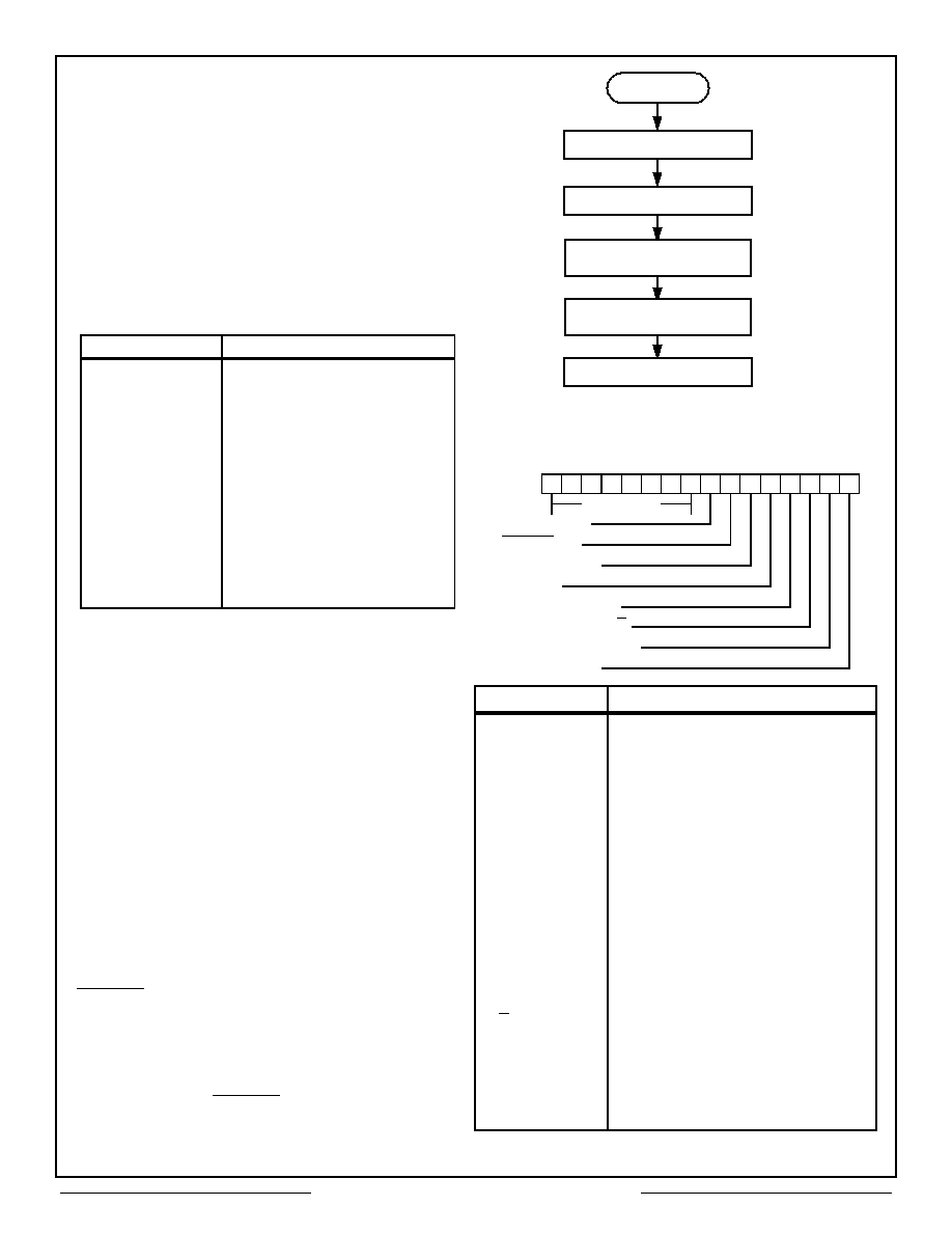
BC OPERATION
Initialization of the CT2553 via a Reset or by
setting the appropriate Configuration Register bits
will result in placing the CT2553 in the BC
operating mode.
BC MEMORY CONFIGURATION. The user
configures the memory by: (1) writing the start
address of the Descriptor Stack into the Current
Area Stack Point location; (2) loading the fourth
word of each Descriptor Stack Entry (DSE) with
the start location of each message block; and (3)
loading the Message Counter with the total
number of messages to be transmitted. Note that
the Message Count must be written in 1's
compliment. For example, to transmit one
message, load OOFE(H) (See Table 3, BC
Memory Map).
If both map areas A and B are utilized, this
procedure must be performed for each area. Note
that the Stack Pointer and Message Counter
locations are fixed; Message Block locations are
user-defined.
Each message block must be proceeded by a BC
Control Word (See Figure 14). This word informs
the CT2553 as to the format of the message
transfer. Bit 1 of the Control Word defines whether
the following message to RT 31 is to be issued in
Broadcast Mode or whether RT 31 is a unique
terminal. Memory locations must be reserved at
the end of each message for: (1) a Loop Back
Word; (2) RTU Status Word(s); and (3) received
Data words. See Figure 16, BC Message
Formats.
Message blocks may be loaded anywhere in the
non-fixed area of the shared RAM. However, each
data block may not cross a 256 word boundary
(i.e., bit 8 of the starting address of the message
block must match bit 8 of the address of the last
word of the message block).
ADDITIONAL FEATURES. The Configuration
Register ≠ STOP ON ERROR bit can be set. This
causes the CT2553 to halt operation at the end of
the current message transfer if an error is
detected. In addition, setting the Interrupt Mask
Register bits will result in a low pulse on the
Interrupt (INT) pin with each occurrence of the
respective error, end of message or end of
message frame condition (See Configuration
Register and Interrupt Register sections).
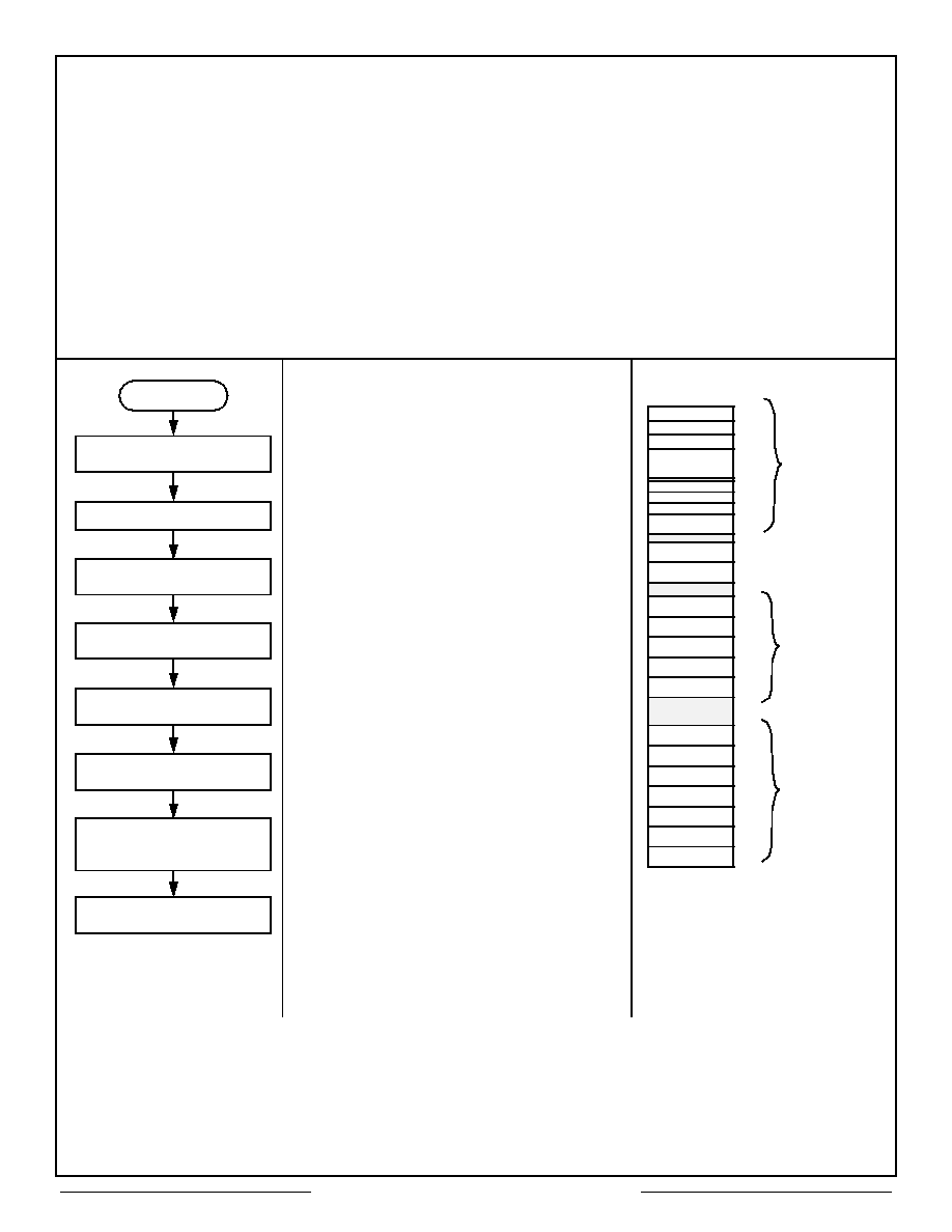
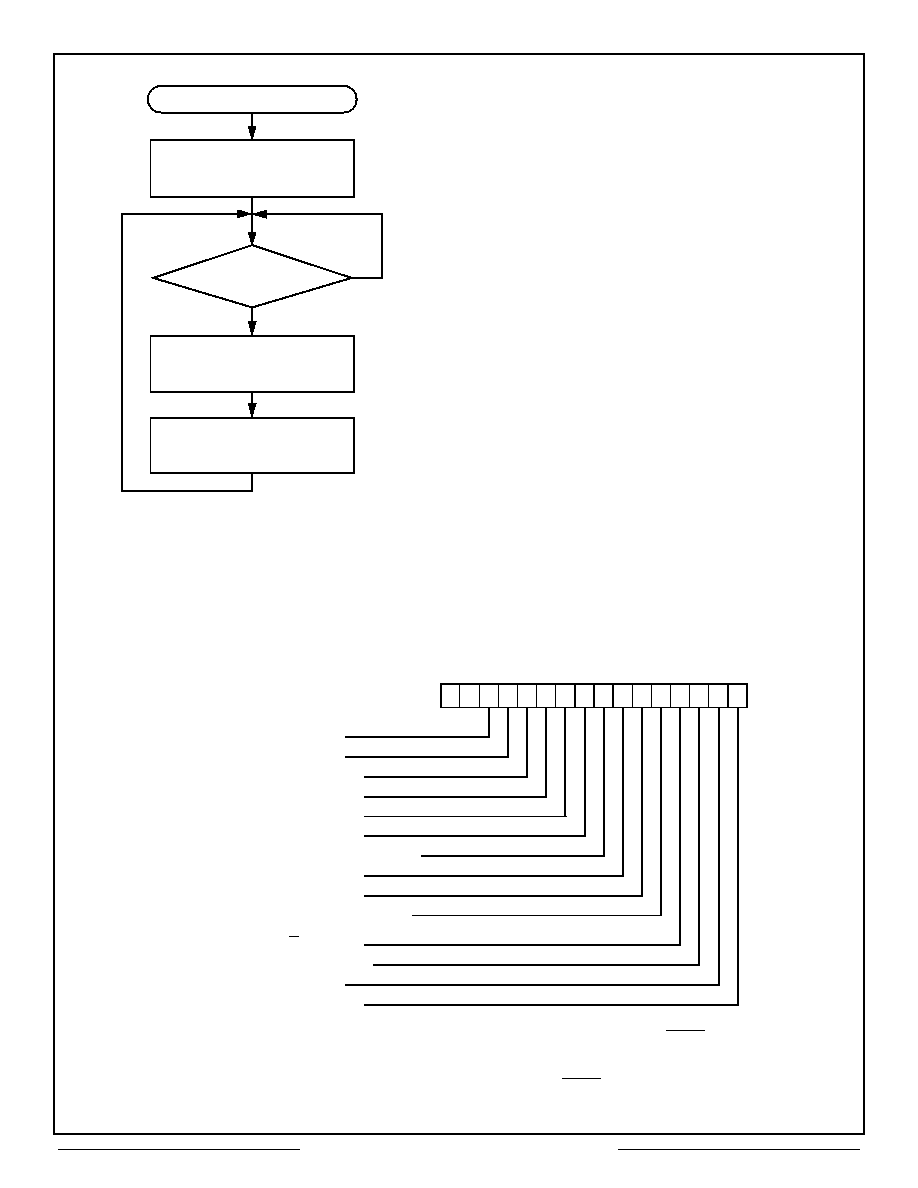
BC TRANSFER-START SEQUENCE
After setting the CONTROLLER START bit in the
Start/Reset Register, the CT2553 takes the
following actions:
1. Reads the Current Area Stack Pointer for the
address of the Descriptor Stack Entry (DSE).
2. Stores an SOM (Start of Message) flag in the
Block Status word to indicate a transfer
operation in progress.
3. Writes the Time Tag value into the Descriptor
Stack (See Time Tag).
4. Reads the Data Block Address from the fourth
location of the DSE.
5. Starts the MIL-STD-1553 message transfer.
Upon completion of the MIL-STD-1553 message
transfer, the CT2553:
1. Generates an End Of Message (EOM) or Error
(if applicable) interrupt if enabled.
2. Reads the Stack Pointer for the address of the
DSE.
3. Updates the Block Status Word; resets SOM,
sets EOM, and sets any applicable Error bits.
4. Writes the Time Tag value into the Descriptor
Stack (See Time Tag).
5. Increment Pointers: Stack Pointer incremented
by 4 and Message Count incremented by 1.
6. If more messages remain to be sent, a BC End
Of Message (BCEOM) interrupt occurs (if
enabled).
If an error occurs and Stop On Error has been
enabled, the CT2553 stops initiating BC
Transfer-Start sequences. The Stack Pointer will
point to the next message to be transferred (See
Figure 17).
Table 3 - Typical BC Memory Map
HEX ADDRESS
FUNCTION
Fixed Areas
0100
Stack Pointer A
0101
Message Count A
0104
Stack Pointer B
0105
Message Count B
User Defined Areas
0108-013F
Not Used
0140-017F
Data Block 1
0180-01BF
Data Block 2
01C0-01FF
Data Block 3
∑
∑
∑
∑
0F00-0FFF
Descriptor Stack A
0000-00FF
Descriptor Stack B

Aeroflex Circuit Technology
14
SCDCT2553 REV B 8/6/99 Plainview NY (516) 694-6700
CONTROLLER START
COMMAND RECEIVED
READS STACK POINTER
LOAD BLOCK STATUS WORD
INTO FIRST WORD OF
DESCRIPTOR STACK ENTRY
(SET SOM BIT IN BLOCK
STATUS WORD)
LOAD TIME TAG INTO
SECOND WORD OF
DESCRIPTOR
STACK ENTRY
ADDRESS FROM FOURTH WORD
OBTAIN DATA BLOCK
DETERMINE TYPE OF TRANSFER
READ CONTROL WORD TO
UPDATE BLOCK STATUS WORD
UPDATE TIME TAG
INCREMENT STACK
POINTER BY FOUR.
DECREMENT
MESSAGE COUNT
TRANSFERRED OK
DATA BLOCK
?
TRANSFERRED OK
STOP ON
?
ERROR SET
YES
NO
NO
YES
NO
MORE MESSAGES
?
TO SEND
YES
ISSUE BC EOM
STOP
Figure 17 ≠ BC Sequence of Operation
TRANSFER DATA TO/FROM
1553 BUS
Aeroflex Circuit Technology
15
SCDCT2553 REV B 8/6/99 Plainview NY (516) 694-6700
LOAD STACK POINTER
LOAD MESSAGE COUNTER WITH
1's COMPLEMENT OF MESSAGE
COUNT = FD (HEX)
START
Figure 18a ≠ BC Set-Up
Example for Two
Message Transfer
BC SETUP IMPLEMENTATION EXAMPLE
Figure 18a-c shows the BC mode examples for
two message transfers, BASIC setup, and BC
memory setup.
LOAD CONFIGURATION
REGISTER (BC MODE)
LOAD STARTING ADDRESS OF
FIRST MESSAGE INTO STACK
LOAD STARTING ADDRESS OF
SECOND MESSAGE INTO STACK
LOAD FIRST MESSAGE
INTO MEMORY
LOAD SECOND MESSAGE
INTO MEMORY
LOAD START REGISTER
WITH THE VALUE 02
Figure 18b ≠ Sample
Figure 18c ≠ BC SET-UP
BC Set-Up Instructions
Memory Map
GIVEN:
1. All values are in hex.
2. Map Area "A" is used and located from Address 0000 to Address
00FF.
3. Message 1 located at Address 0140, is a TRANSMIT Command
to RT# 1, Subaddress #1, Word Count = 1, transmitted on
BUS A.
4. Message 2 located at Address 0180, is a RECEIVE Command to
RT#3, Subaddress #1, Word Count = 3, transmitted on BUS B.
5. Configuration Register is assumed to be memory mapped at
location 2001. START/RESET Register is memory mapped at
location 2003.
MOV
2003,
0001
;
Issue Reset
MOV
2001,
0FFF
;
Initialize Configuration Register
MOV
0100,
0000
;
Initialize Stack Pointer
MOV
0101,
00FD
;
Initialize Message Count
MOV
0003,
0140
;
Load Start Address Of Message #1
MOV
0007,
0180
;
Load Start Address Of Message #2
MOV
0140,
0080
;
Load BC Control Word Message #1
MOV
0141,
0C21
;
Load Command Word Message #1
MOV
0180,
0000
;
Load BC Control Word Message #2
MOV
0181,
1823
;
Load Command Word Message #2
MOV
0182,
1111
;
Load Data Word #1 Message #2
MOV
0183,
2222
;
Load Data Word #2 Message #2
MOV
0184,
3333
;
Load Data Word #3 Message #2
MOV
2003,
0002
;
Issue "Start"
0000
01
40
0003
Descriptor
Stack Entries
01
80
0007
0000
0100
00FD
0101
00
80
0140
0C
21
**
Message #1
*
*
00
00
0180
18
23
11
11
22
22
Message #2
33
33
**
*
* Left empty for RTU's status response.
** Loop Back word.
Aeroflex Circuit Technology
16
SCDCT2553 REV B 8/6/99 Plainview NY (516) 694-6700
RTU OPERATION
The RTU mode is selected by resetting the
CT2553 and setting the appropriate bits in the
Configuration Register.
RTU MEMORY CONFIGURATION. The user
configures the memory by:
1. Writing the start address of the Descriptor
Stack into the Stack Pointer location and
2. Setting up the Look-Up Table as described
below.
If both map areas (A and B) are utilized, this
procedure must be performed for each area. Note
that the Stack Pointer and Look-Up Table
locations are fixed; Data Block(s) locations are
user-defined. Message blocks may be loaded
anywhere in the non-fixed areas of the shared
RAM. However, each data block may not cross a
256 word boundary (i.e., bit 8 of the starting
address of the message block must match bit 8 of
the address of the last word of the message
block). An example of a typical RTU Memory Map
is given in Table 4. Figure 19 shows the RTU
Initialization steps.
RTU LOOK-UP TABLE. The RTU mode uses a
Look-Up Table in order to map the Data Blocks
based upon incoming 1553 Command Words.
The CT2553 uses the T/R and Subaddress fields
to address the Look-Up Table. Each Look-Up
Table (A and B) location contains a user-defined
Data Block Pointer to an associated Data Block
(See Figures 20 and 21).
Note: The Data Block and Stack Pointers are
maintained internally using an
8-BIT-REGISTER for the HIGH BYTE and an
8-BIT COUNTER for the LOW BYTE; the high
byte remains constant (user value) while the low
byte will wrap around from FF(H) to 00(H). For
example: a current Pointer value of 10 FF(H)
will increment to 10 00(H) and not 11 00(H).
The first 32 words of the Look-Up Table are
reserved for Data Blocks associated with Receive
Commands (T/R bit = 0). The remaining 32 words
are reserved for Data Blocks associated with
Transmit Commands (T/R bit = 1).
Mode Commands with data are mapped in the
same manner as non-mode commands. A
Synchronize With Data command maps to the
first or thirty-second Table entry (depending upon
subaddress: all 0's or all 1's), while a Transmit
Vector Word command points to the thirty-third or
sixty-fourth entry.
Table 4 ≠ Typical RTU Memory Map
HEX ADDRESS
FUNCTION
Fixed Areas
0100
Descriptor Stack Pointer A
0101
Reserved
0104
Descriptor Stack Pointer B
0105
Reserved
0108-013F
Spare
0140-017F
Look-Up Table A
01C0-01FF
Look-Up Table B
User Defined Areas
0180-019F
Data Block 1
01A0-01BF
Data Block 2
0200-021F
Data Block 3
∑
∑
∑
∑
0EE0-0EFF
Data Block 107
0000-00FF
Descriptor Stack A
0F00-0FFF
Descriptor Stack B
START
ISSUE RESET COMMAND
INITIALIZE STACK POINTER
SET UP DATA BLOCKS
WAIT FOR 1553 COMMAND
SET UP LOOK-UP TABLE(S)
DATA BLOCK ASSIGNMENTS
Figure 19 ≠ RTU Initialization
INITIALIZE INTERRUPT
MASK REGISTER
SET CONFIGURATION
REGISTER TO RTU MODE
START REGISTER
Aeroflex Circuit Technology
17
SCDCT2553 REV B 8/6/99 Plainview NY (516) 694-6700
RTU MESSAGE BLOCK TRANSFER SEQUENCE
RTU message transfer operations begin
automatically upon receipt of a valid command
word from the 1553 bus. A message transfer
takes the form of an RTU Start Of Message
(SOM) cycle followed by the 1553 Message
Transfer Cycle and an RTU End Of Message
(EOM) cycle (See Figure 22).
During the RTU SOM cycle, the CT2553 the
following actions:
1. Loads the 1553 command word.
2. Reads the current area Stack Pointer to get the
address of the current Descriptor Stack Entry
(DSE).
3. Stores an SOM flag into the Block Status Word
to indicate a transfer in progress.
4. Writes the Time Tag value into the the
Descriptor Stack.
5. Stores the Command Word received.
6. Reads the associated Data Block Address from
the (current area) Look-Up Table.
The MESSAGE TRANSFER CYCLE refers to the
actual transfer of the 1553 message under control
of the CT2553. The CT2553 transfers data to and
from the memory on a word-by-word basis.
Upon completion of the message transfer, the
CT2553 executes an RTU End Of Message
(EOM) cycle during which the CT2553:
1. Generates an EOM or Error interrupt (if
enabled).
2. Updates the Block Status Word: clears SOM,
sets EOM, and any appropriate error bits.
3. Writes the Time Tag value into the Descriptor
Stack.
4. Increments the Stack Pointer by 4.
Figure 22 ≠ RTU Message Transfer
Operation
MESSAGE COMPLETE
GENERATE EOM INTERRUPT AND
CONDITION DETECTED
ERROR INTERRUPT IF ERROR
INCREMENT STACK POINTER
BY FOUR
UPDATE BLOCK STATUS WORD
AND TIME TAG
TRANSFER DATA TO/FROM
1553 INTERFACE DEVICE
READ LOOK-UP TABLE USING
AREA BIT B/A
T/R SUBADDRESS CURRENT
UPDATE DESCRIPTOR STACK
TAG AND COMMAND WORD
BLOCK STATUS WORD, TIME
READ STACK POINTER
1553 COMMAND WORD
RECEIVED
?
NO
YES
WAIT FOR NEXT
1553 COMMAND
15
7 6 5 4 3 2 1 0
0 0 0 0 0 0 0 1
1
CURRENT AREA B/A
T/R (from command word)
SUB-ADDRESS (command word)
Figure 20 ≠ RTU Look-Up Address
RECEIVED COMMAND WORDS
DATA BLOCK
T/R
SUBADD
WORD
COUNT
LOOK-UP
TABLE (A)
ADDRESS
DATA BLOCK
0
00000
XXXXX
0140
USER DEFINED
0
00001
XXXXX
0141
USER DEFINED
0
00010
XXXXX
0142
USER DEFINED
*
64 LOCATIONS
*
*
1
11110
XXXXX
017E
USER DEFINED
1
11111
XXXXX
017F
USER DEFINED
Figure 21 ≠ Look-Up Table Example
Aeroflex Circuit Technology
18
SCDCT2553 REV B 8/6/99 Plainview NY (516) 694-6700
ADDITIONAL FEATURES. Four 1553 Status
Word flags can be programmed via the
appropriate Configuration Register bits. In
addition, setting Interrupt Mask Register bits will
result in a low pulse on the Interrupt (INT) pin
with each occurrence of the respective error or
end of message condition. (See Configuration
Register and Interrupt Register sections.)
THIS RT: Each command appearing on either
1553 Bus is decoded and tested for
Manchester/protocol errors. If the CT2553
receives a valid command word containing a
RTU address equivalent to the RTAD0-RTAD4
inputs (pins 10, 9, 50, 49, and 11, respectively),
THIS-RT (pin 55) will be pulsed low. This signal
can be used to identify specific 1553 commands.
This signal is also active in the BC mode.
Command Illegalization (Optional). The CT2553
has the capability to illegalize MIL-STD-1553
mode commands. In addition, valid non-mode
commands can be illegalized based upon the
Command Word subaddress field. An illegal
command is identified by driving the Illegal
Command, ILLCMD (pin 12) input low. The
CT2553 multiplexes the Word Count and
Subaddress fields (pins SA/MC0 - SA/MC4).
The CT2553 responds to illegalized commands
by transmitting its Status Word with the Message
Error bit set. No data words are transmitted;
received words, however, are placed in the
shared RAM locations indicated by the current
area Look-Up Table.
Upon receipt of a valid mode command, the
CT2553 will output the Command Word-Word
Count field and set the Latched Mode Command
(LMC) output to a logic 1. Upon receipt of a valid
non-mode command, the CT2553 will output the
Command Word-Subaddress field and set the
Latched Mode Command (LMC) output to a
logic 0.
An external PROM can be used for command
illegalization by decoding the word
count/subaddress, LMC and Broadcast Received
(BCSTRCV) bits and driving ILLCMD low where
appropriate (See Figure 23).
BUSY BIT. If the user asserts the BUSY bit low
in the Configuration Register, the CT2553 will
respond with a Status Word with the BUSY bit
set. In addition, no data words will be transferred
from the shared RAM as indicated by the
corresponding value in the current area Look-Up
Table. The CT2553 will transfer data associated
with a Receive Command into memory but will
not transmit data out onto the MIL-STD-1553 bus
when busy upon receipt of a Transmit Command.
LMC
SA/MC0-4, T/R
ILLCMD
LATCHED UNTIL NEXT VALID COMMAND WORD RECEIVED
VALID UNTIL NEXT VALID COMMAND WORD RECEIVED
t1
Mode Command Illegalization Timing
SYMBOL
DESCRIPTION
MIN
MAX
UNITS
t1
LMC to ILLCMD latch
250
-
ns
Figure 23 ≠ Mode Command/Sub-Address Illegalization Timing
Aeroflex Circuit Technology
19
SCDCT2553 REV B 8/6/99 Plainview NY (516) 694-6700
MT OPERATION
Initiate a Reset in order to initialize the CT2553.
Configure the CT2553 as a Bus Monitor (MT) by
setting the appropriate Configuration Register
Bits. See Figure 24 for MT initialization Steps.
MT MEMORY CONFIGURATION. The user
configures the memory by writing the start
address for 1553 data storage into the Stack
Pointer location. The Monitor Stack will
automatically wrap around once the RAM has
been filled (i.e., location FFF(H) is followed by
location 0000). An example of a typical MT
Memory Map 4 given in Table 5.
MT START SEQUENCE. After setting the
CONTROLLER START bit in the Start/Reset
Register, the CT2553 takes the following actions:
1. Reads the start address for 1553 data storage
from the Stack Pointer location. The Stack
Pointer location(s) will be overwritten with 1553
data once the MT mode has begun and 1553
data is written into locations 0100(H) and
0101(H)].
2. Stores the received 1553 word into memory.
3. Increments the Stack Pointer by 1.
4. Generates an Identification Word and stores
this value into memory.
5.Repeats steps 2-4 until a Reset condition
occurs.
MT IDENTIFICATION WORD. The Identification
word provides the CPU with information pertaining
to the received 1553 word. Its format is shown in
Figure 25, This information allows the user to
analyze the 1553 data.
THIS-RT: Each command appearing on either
1553 Bus is decoded and tested for
Manchester/protocol errors. If the CT2553
receives a valid command word containing a
Command Sync and a RTU address equivalent to
the RTAD0-RTAD4 inputs (pins 10, 9, 50, 49, and
11, respectively), THIS-RT (pin 55) will be pulsed
low. This signal can be used to identify specific
1553 commands or for switching to RTU mode
upon receipt of a command to this address.
Table 5 ≠ Typical MT Memory Map
HEX ADDRESS
FUNCTION
0000
First Received 1553 Word
0001
First Identification Word
0002
Second Received 1553 Word
0003
Second Identification Word
0004
∑
0005
∑
0006
∑
∑
∑
∑
∑
0100
Stack Pointer (Fixed location)
∑
∑
∑
∑
FFFF
∑
MSB
LSB
15
8 7 6 5 4 3 2 1 0
1
GAP TIME
WORD FLAG
THIS RT
BROADCAST
ERROR
COMMAND SYNC
1553 CHANNEL A/B
CONTIGUOUS DATA
MODE CODE
BIT NAME
DEFINITION
GAP TIME
Indicates the time between receipt of the
previous and current words.Time is
indicated in 0.5µs increments for a
maximum of 128 µs and goes to FF over
128µs. (See Word Gap bit.)
WORD FLAG
Always logic 1.
THIS RT
Logic 0 indicates RT address field of the
associated command or Status Word
matches the RT address field of the
CT2553.
BROADCAST
Logic 0 indicates the RTU address field of
the command or Status Word
corresponds to address 31 (decimal).
ERROR
Logic 1 indicates Manchester, Parity,
Sync and/or low bit counter.
COMMAND SYNC
Logic 1 indicates 1553 Command or
Status Word sync field. (Logic 0 indicates
a Data Word sync field in received word.)
1553 CHANNEL
A/B
Indicates word received on 1553 Bus A
(1) or Bus B (0).
CONTIGUOUS
DATA
Logic 1 indicates the word was received
within 2µs of the previous word. If logic 0,
bits 8-15 contain the measured gap
between the words.
MODE CODE
When logic 1, the data transferred is a
mode code command.
Figure 25 ≠ MT Identification Word
START
ISSUE RESET COMMAND
CLEAR RAM
ISSUE START COMMAND
INITIALIZE STACK POINTER
SET CONFIGURATION
REGISTER TO MT MODE
Figure 24 ≠ MT Initialization
Aeroflex Circuit Technology
20
SCDCT2553 REV B 8/6/99 Plainview NY (516) 694-6700
MT DATA STORAGE. Figure 26 shows the steps
in a MT data Storage operation.
INTERRUPTS: SA/MC - 0 (pin 13), SA/MC - 1
(pin 52) and SA/MC - 2 (on 52) represents B6,
B7, and B8 counter outputs in the MT mode. B6
counts every 32 words transferred, B7 every 64
words, and B8 every 128 words. These counter
outputs can be used to generate interrupts to the
subsystem to insure proper servicing of Memory.
The Data Word and Identification Word transfers
increment the counter by two.
BUILT-IN-TEST WORD (RTU MODE)
The CT2553 contains a 14 bit Built-In-Test (BIT)
word register which stores information about the
condition of the RTU. When a Mode Command is
received to transmit BIT word, the contents of this
register are transmitted over the 1553 data bus.
Figure 27 shows the meaning of each bit in the
BIT register. Information is included regarding
transmitter timeouts, loop test failures, transmitter
shutdown, subsystem handshake failure, and the
results of individual message validations.
MODE CODES
The CT2553 implements all mode codes
applicable to dual redundant systems. Mode
codes can also be illegalized using the
appropriate I/O signals. Mode command
illegalization and handling are detailed in the RTU
Operation section and listed in Table 6.
GET STACK POINTER FROM
WORD 100 IN RAM AND
STORE IN INTERNAL REGISTER
START COMMAND ISSUED
STORE RETREIVED 1553 WORD
IN RAM, INCREMENTS INTERNAL
ADDRESS REGISTER
Figure 26 ≠ MT Data Storage Operation
STORE IDENTIFICATION WORD
IN RAM, INCREMENT INTERNAL
ADDRESS REGISTER
NO
WORD TRANSFERRED
ACROSS 1553 BUS
?
YES
15 14 13 12 11 10 9 8 7 6 5 4 3 2 1 0
0 0
CHAN B XMITTER TIMEOUT
CHAN A XMITTER TIMEOUT
CHAN B LOOP TEST FAILURE
CHAN A LOOP TEST FAILURE
CHAN B XMITTER SHUTDOWN
CHAN A XMITTER SHUTDOWN
NON-MODE BROADCAST CMD TO XMIT
MESSAGE HIGH WORD COUNT
MESSAGE LOW WORD COUNT
ILLEGAL MODE CODE OR ILLEGAL
BROADCAST WITH MODE CODE
MODE CODE OR T/R ERROR
CHAN A/B LOOP TEST FAILURE
HANDSHAKE FAILURE
CHAN A/B XMITTER TIMEOUT
Notes:
(1) Bits 0-2 and 10-13 are latched and only cleared by a mode reset command or a master RESET.
(2) Bits 3-7 are cleared at the start of each new message and updated at the end of the message. They
reflect the present command word.
(3) Bits 8-9 are set by the mode command for Transmitter Shutdown and are cleared by the mode
command for Override Transmitter Shutdown, Reset RT or a master RESET.
Figure 27 ≠ Built-In-Test Word (RTU Mode)

Aeroflex Circuit Technology
21
SCDCT2553 REV B 8/6/99 Plainview NY (516) 694-6700
DYNAMIC BUS CONTROL (00000)
MESSAGE SEQUENCE = DBC * STATUS
The CT2553 responds with status. If the subsystem wants control of the bus, it must set DBACC within 2.5us after NBGRT.
ERROR CONDITIONS
1. Invalid Command. No response, command ignored.
2. Command Followed by Data Word. No status response. Bits set: message error (SW), High word Count (BIT Word).
3. T/R bit Set to Zero. No status response. Bits set: message error (SW), T/R Error (Bit Word).
4. Zero T/R bit and Broadcast Address. No status response. Bits set: message error, broadcast received (SW), Illegal Mode Code, T/R
Error (BIT Word).
5. Broadcast Address. No status response. Bits set: message error, broadcast received (SW), Illegal Mode Code (BIT Word).
SYNCHRONIZE WITHOUT DATA WORD (00001)
MESSAGE SEQUENCE = SYNC * STATUS
The CT2553 responds with status. If sent as a broadcast, the broadcast receive bit will be set and status response suppressed.
ERROR CONDITIONS
1. Invalid Command. No response, command ignored.
2. Command Followed by Data Word. No status response. Bits set: message error (SW), High Word Count (BIT Word).
3. T/R bit Set to Zero. No status response. Bits set: message error (SW), T/R Error (BIT Word).
4. Zero T/R bit and Broadcast Address. No status response. Bits set: message error, broadcast received (SW), Illegal Mode Code, T/R
Error (BIT Word).
TRANSMIT STATUS WORD (00010)
MESSAGE SEQUENCE = TRANSMIT STATUS * STATUS
The status and BIT word registers are not altered by this command and contain the resulting status from the previous command.
ERROR CONDITIONS
1. Invalid Command. No response, command ignored.
2. Command Followed by Data Word. No status response. Bits set: message error (SW), High Word Count (BIT Word).
3. T/R bit Set to Zero. No status response. Bits set: message error (SW), T/R Error (BIT Word).
4. Zero T/R bit and Broadcast Address. No status response. Bits set: message error, broadcast received (SW), Illegal Mode Code, T/R
Error (BIT Word).
5. Broadcast Address. No status response. Bits set: message error, broadcast received (S/W), Illegal Mode code, T/R Error (BIT Word).
INITIATE SELF-TEST (00011)
MESSAGE SEQUENCE = SELF TEST * STATUS
The CT2553 responds with a status word. If the command was broadcast, the broadcast received bit is set and status transmission
suppressed. Short-loop test is initiated on the status word transmitted. If the test fails, an RT fail flag is generated.
ERROR CONDITIONS
1. Invalid Command. No response, command ignored.
2. Command Followed by Data Word. No status response. Bits set: message error (SW), High Word Count (BIT Word).
3. T/R bit Set to Zero. No status response. Bits set: message error (SW), T/R Error (BIT Word).
4. Zero T/R bit and Broadcast Address. No status response. Bits set: message error, broadcast received (SW), T/R Error (BIT Word).
5. Faulty Test. Bits set: terminal flag (SW), A/B Loop Test Fail, Current 1553 Bus (A or B) Loop Test Fail (BIT Word).
TRANSMITTER SHUTDOWN (00100)
MESSAGE SEQUENCE - SHUTDOWN * STATUS
This command is only used with dual redundant bus systems. The CT2553 responds
with status. At the end of the status transmission, the CT2553 inhibits any further transmission from the dual redundant channel. Once
shutdown, the transmitter can only be re-activated by Override Transmitter Shutdown or RESET RT commands.
ERROR CONDITIONS
1. Invalid Command. No response, command ignored.
2. Command Followed by Data Word. No status response. Bits set: message error (SW), High Word Count (BIT Word).
3. T/R bit Set to Zero. No status response. Bits set: message error (SW), T/R Error BIT Word).
4. Zero T/R bit and Broadcast Address. No status response. Bits set: message error, broadcast received (SW), Illegal Mode Code, T/R
Error (BIT Word).
Table 6 ≠ Mode Codes

Aeroflex Circuit Technology
22
SCDCT2553 REV B 8/6/99 Plainview NY (516) 694-6700
OVERRIDE TRANSMITTER SHUTDOWN (00101)
MESSAGE SEQUENCE - OVERRIDE SHUTDOWN - STATUS
This command is only used with dual redundant bus systems. The CT2553 responds with status. At the end of the status transmission, the
CT2553 re-enables the transmitter of the redundant bus. If the command was broadcast, the broadcast received bit is set and status
transmission is suppressed.
ERROR CONDITIONS
1. Invalid Command. No response, command ignored.
2. Command Followed by Data Word. No status response. Bits set: message error (SW), High Word Count (BIT Word).
3. T/R bit Set to Zero. No status response. Bits set: message error (SW), T/R Error (BIT Word).
4. Zero T/R bit and Broadcast Address. No status response. Bits set: message error, broadcast received (SW), Illegal Mode Code, T/R
Error (BIT Word).
INHIBIT TERMINAL FLAG BIT (00110)
MESSAGE SEQUENCE - INHIBIT TERMINAL FLAG * STATUS
The CT2553 responds with status and inhibits further internal or external setting of the terminal flag bit in the status register. Once the
terminal flag has been inhibited, it can only be reactivated by an Override Inhibit Terminal Flag or Reset RT command. If the command was
broadcast, the broadcast received bit is set and status transmission is suppressed.
ERROR CONDITIONS
1. Invalid Command. No response, command ignored.
2. Command Followed by Data Word. No status response. Bits set: message error (SW), High Word Count (BIT Word).
3. T/R bit Set to Zero. No status response. Bits set: message error (SW), T/R Error (BIT Word).
4. Zero T/R bit and Broadcast Address. No status response. Bits set: message error, broadcast received (SW), T/R Error (BIT Word).
OVERRIDE INHIBIT TERMINAL FLAG BIT (00111)
MESSAGE SEQUENCE - OVERRIDE INHIBIT TERMINAL FLAG * STATUS
The RTU responds with status and reactivates the terminal flag bit in the status register. If the command was broadcast, the broadcast
received bit is set and status transmission is suppressed.
ERROR CONDITIONS
1. Invalid Command. No response, command ignored.
2. Command Followed by Data Word. No status response. Bits set: message error (SW), High Word Count (BIT Word).
3. T/R bit Set to Zero. No status response. Bits set: message error (SW), T/R Error (BIT Word).
4. Zero T/R bit and Broadcast Address. No status response. Bits set: message error, broadcast received (SW), T/R Error (BIT Word).
RESET REMOTE TERMINAL (01000)
MESSAGE SEQUENCE - RESET REMOTE TERMINAL * STATUS
The CT2553 responds with status and internally resets. Transmitter shutdown, mode commands, and inhibit terminal flag commands will be
reset. If the command was broadcast, the broadcast received bit is set and the status word is suppressed.
ERROR CONDITIONS
1. Invalid Command. No response, command ignored.
2. Command Followed by Data Word. No status response. Bits set: message error (SW), High Word Count (BIT Word).
3. T/R bit Set to Zero. No status response. Bits set: message error (SW), T/R Error (BIT Word).
4. Zero T/R bit and Broadcast Address. No status response. Bits set: message error, broadcast received (SW), T/R Error (BIT Word).
RESERVED MODE CODES (01001-01111)
MESSAGE SEQUENCE = RESERVED MODE CODES * STATUS
The CT2553 responds with status. If the command is illegalized through an optional PROM, the message error bit is set and only the status
word is transmitted.
ERROR CONDITIONS
1. Invalid Command. No response, command ignored.
2. Command Followed by Data Word. No status response. Bits set: message error (SW), High Word Count (BIT Word).
3. T/R bit Set to Zero. No status response. Bits set: message error (SW), Illegal Mode Code (BIT Word).
4. Zero T/R bit and Broadcast Address. No status response. Bits set: message error, broadcast received (SW), Illegal Mode Code (BIT
Word).
Table 6 ≠ Mode Codes (continued)

Aeroflex Circuit Technology
23
SCDCT2553 REV B 8/6/99 Plainview NY (516) 694-6700
TRANSMIT VECTOR WORD (10000)
MESSAGE SEQUENCE - TRANSMIT VECTOR WORD * STATUS VECTOR WORD
The CT2553 transmits a status word followed by a vector word. The contents of the vector word (from the subsystem) are enabled onto
DBO-DB15 with BUSREQ after the command transfer (same as data word in a normal transmit command).
ERROR CONDITIONS
1. Invalid Command. No response, command ignored.
2. Command Followed by Data Word. No status response. Bits set: message error (SW) High Word Count (BIT Word).
3. T/R bit Set to Zero. No status response. Bits set: message error (SW), T/R Error, Low Word Count (BIT Word).
4. Zero T/R bit and Broadcast Address. No status response. Bits set: message error, broadcast received (SW), Illegal Mode Code, T/R
Error, Low Word Count (BIT Word).
5. Broadcast Address. No status response. Bits set: message error, broadcast received (SW), Illegal Mode code, (BIT Word).
SYNCHRONIZE WITH DATA WORD (10001)
MESSAGE SEQUENCE - SYNCHRONIZE DATA WORD * STATUS
The data word received following the command word is transferred to the subsystem. The status register is then enabled and its contents
transferred onto the data bus and transmitted. If the command was broadcast, the broadcast received bit is set and status transmission is
suppressed.
ERROR CONDITIONS
1. Invalid Command. No response, command ignored.
2. Command Not Followed by Data Word. No status response. Bits set: message error (SW), Low Word Count (BIT Word).
3. Command followed by too many Data Words. No status response. Bits set: message error (SW), High Word Count (BIT word).
4. Command T/R bit Set to One. No status response. Bits set: message error (SW), T/R Error, High Word Count (BIT Word).
5. Command, T/R bit Set to One and Broadcast Address. No status response. Bits set: message error, broadcast received (SW), High
Word Count, T/R Error (BIT Word).
TRANSMIT LAST COMMAND (10010)
MESSAGE SEQUENCE = TRANSMIT LAST COMMAND * STATUS LAST COMMAND
The status and BIT word registers are not altered by this command. The SW contains the status from the previous command. The data
word transmitted contains the previous valid command (providing it was not another TRANSMIT LAST COMMAND).
ERROR CONDITIONS
1. Invalid Command. No response, command ignored.
2. Command Followed by Data Word. No status response. Bits set: message error (SW).
3. T/R bit Set to Zero. No status response. Bits set: message error (SW), T/R Error, Low Word Count (BIT Word).
4. Zero T/R bit and Broadcast Address. No status response. Bits set: message error, (SW), Illegal Mode Code T/R Error (BIT Word).
5. Broadcast Address. No status response. Bits set: message error, broadcast received (SW), Illegal Mode Code (BIT Word).
TRANSMIT BIT WORD (10011)
MESSAGE SEQUENCE - TRANSMIT BIT WORD * STATUS BIT WORD
The CT2553 transmits a status word followed by the BIT word . When activated, BITEN allows the subsystem to latch the BIT word on the
parallel data bus. The BIT word is not altered by this command; however, the next SW will reflect errors in this transmission.
ERROR CONDITIONS
1. Invalid Command. No response, command ignored.
2. Command Followed by Data Word. No status response. Bits set: message error (SW).
3. T/R bit Set to Zero. No status response. Bits set: message error (SW), T/R Error, Low Word Count (BIT Word).
4. Zero T/R bit and Broadcast Address. No status response. Bits set: message error, broadcast received (SW), Illegal Mode Code, T/R
Error, Low Word Count (BIT Word).
5. Broadcast Address. No status response. Bits set: message error, broadcast received (SW), Illegal Mode code, (BIT Word).
Table 6 ≠ Mode Codes (continued)

Aeroflex Circuit Technology
24
SCDCT2553 REV B 8/6/99 Plainview NY (516) 694-6700
SELECTED TRANSMITTER SHUTDOWN (10100)
MESSAGE SEQUENCE - TRANSMITTER SHUTDOWN DATA * STATUS
The data word received is transferred to the subsystem and status is transmitted. If the
command was broadcast, the broadcast received bit is set and status transmission suppressed. Intended for use with RTs with more than
one dual redundant channel.
ERROR CONDITIONS
1. Invalid Command. No response, command ignored.
2. Command Not Followed by Data Word. No status response. Bits set: message error (SW), High Word Count, Illegal Mode Code (BIT
Word).
3. Command Followed by too many Data Words. No status response. Bits set: message error (SW), Low Word Count, Illegal Mode Code
(BIT Word).
4. Command T/R bit Set to One. No status response. Bits set: message error (SW), Illegal Mode Code, High word count (BIT Word).
5. Command T/R bit Set to One and Broadcast Address. No status response. Bits set: message error, broadcast received (SW), Illegal
Mode Code, High Word Count (BIT Word).
OVERRIDE SELECTED TRANSMITTER SHUTDOWN (10101)
MESSAGE SEQUENCE - TRANSMITTER SHUTDOWN DATA * STATUS
The data word received after the command word is transferred to the subsystem. If the
command was broadcast, the broadcast received bit is set and status transmission suppressed.
ERROR CONDITIONS
1. Invalid Command. No response, command ignored.
2. Command Not Followed by Data Word. No status response. Bits set: message error (SW), Low Word Count, Illegal Mode Code (BIT
Word).
3. Command Followed by too many Data Words. No status response. Bits set: message error (SW), High Word Count, Illegal Mode Code
(BIT Word).
4. Command T/R bit Set to One. No status response. Bits set: message error (SW), Illegal Mode Code, High Word Count (Bit Word).
5. Command T/R bit Set to One and Broadcast Address. No status response. Bits set: message error, broadcast received (SW), Illegal
Mode Code, High Word Count, T/R (BIT Word).
RESERVED MODE CODES
MESSAGE SEQUENCE = RESERVED MODE CODE (T/R = 1) * STATUS
RESERVED MODE CODE (T/R = 0) * STATUS
The CT2553 responds with status. If the command was broadcast, the broadcast received bit is set and status transmission suppressed.
ERROR CONDITIONS (T/R = 1)
1. Invalid Command. No response, command ignored.
2. Command Followed by Data Word. No status response. Bits set: message error (SW), High Word Count, Illegal Mode Code (BIT
Word).
ERROR CONDITIONS (T/R = 0)
1. Invalid Command. No response, command ignored.
2. Command not Followed by Contiguous Data Word. No status response. Bits set: message error (SW), High word Count, Illegal Mode
Code (BIT Word).
3. Command Followed by too many Data Words. No status response. Bits set: message error (SW), High Word Count, Illegal Mode Code
(BIT Word).
Table 6 ≠ Mode Codes (continued)
Aeroflex Circuit Technology
25
SCDCT2553 REV B 8/6/99 Plainview NY (516) 694-6700
A02
A01
A00
SSFLAG, SSBUSY, SVCRQST
DBAC, RTU/BC, MT, CTLOUT B/A
MEM/REG
D15-D00
IOEN
SELECT
STRBD
(Internal)
16MHz Clock
RD/WR
READYD
See Note 1
td1
td2
td8
tpw1
td7
td9
DATA LATCHED
Configuration Register Only
DATA VALID
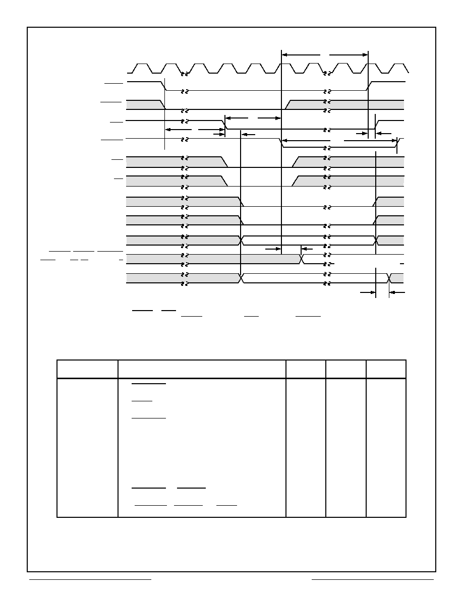
Figure 28 ≠ CPU Writes to Internal Register
CPU Writes to Internal Register
SYMBOL
DESCRIPTION
MIN
MAX
UNITS
td1
READYD low delay (CPU Handshake)
-
150
ns
td2
IOEN high delay (CPU Handshake)
-
20
ns
tpw1
READYD pulse width (CPU Handshake)
50
-
ns
td7
Internal Register delay (write)
-
60
ns
td8
Register Data/Address set-up time
-
30
ns
td9
Register Data/Address hold time
-
0
ns
tr
READYD to STRBD release
-
1.37
µs
tz
(SELECT
∑
STRBD) to IOEN
-
1.8
µs
tz
tr
See Note 2
NOTE:
1. STRBD to IOEN (low) delay is two clock cycles. If contention occurs, delay is two clock cycles following release of bus.
2. CPU must release STRBD within 1.5µs of IOEN going active. READYD will go away within one clock cycle maximum.
Aeroflex Circuit Technology
26
SCDCT2553 REV B 8/6/99 Plainview NY (516) 694-6700
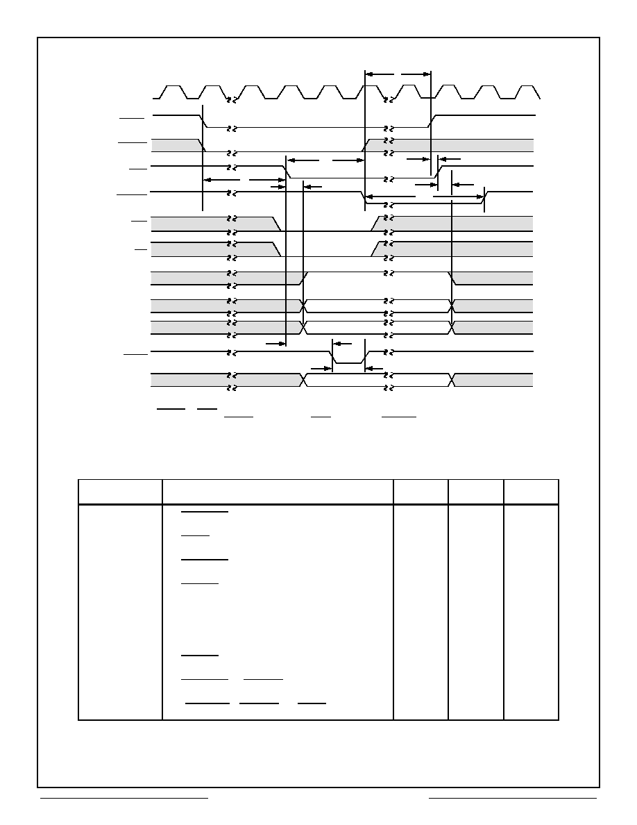
A02
A01
A00
MEM/REG
D15-D00
IOEN
SELECT
STRBD)
(Internal)
16MHz Clock
RD/WR
READYD
See Note 1
td1
td8
tpw1
CPU DATA
EXTLD
td9
VALID
VALID
tpw6
td5
td2
Figure 29 ≠ CPU Writes to External Register
CPU Writes to External Register
SYMBOL
DESCRIPTION
MIN
MAX
UNITS
td1
READYD low delay (CPU Handshake)
-
150
ns
td2
IOEN high delay (CPU Handshake)
-
20
ns
tpw1
READYD pulse width (CPU Handshake)
50
-
ns
td5
EXTLD low delay
50
-
ns
td8
Register Data/Address set-up time
-
30
ns
td9
Register Data/Address set-up time
-
0
ns
tpw6
EXTLD low pulse width
56
-
ns
tr
READYD to STRBD release
-
1.37
µs
tz
(SELECT
∑
STRBD) to IOEN
-
1.8
µs
tz
tr
See Note 2
NOTE:
1. STRBD to IOEN (low) delay is two clock cycles. If contention occurs, delay is two clock cycles following release of bus.
2. CPU must release STRBD within 1.5µs of IOEN going active. READYD will go away within one clock cycle maximum.
Aeroflex Circuit Technology
27
SCDCT2553 REV B 8/6/99 Plainview NY (516) 694-6700
MEMOE
MEM/REG
A15-A00
IOEN
SELECT
STRBD
(Internal)
16MHz Clock
RD/WR
READYD
See Note 1
td1
tpw1
D15-D00
td2
RAM ADDRESS VALID
td4
RAM DATA VALID
MEMCS
Figure 30 ≠ CPU Reads from RAM Timing
CPU Reads from RAM
SYMBOL
DESCRIPTION
MIN
MAX
UNITS
td1
READYD low delay (CPU Handshake)
-
150
ns
td2
IOEN high delay (CPU Handshake)
-
20
ns
tpw1
READYD pulse width (CPU Handshake)
50
-
ns
td4
CPU MEMOE low delay
-
100
ns
tr
READYD to STRBD release
-
1.37
µs
tz
(SELECT
∑
STRBD) to IOEN
-
1.8
µs
NOTE:
1. STRBD to IOEN (low) delay is two clock cycles. If contention occurs, delay is two clock cycles following release of bus.
2. CPU must release STRBD within 1.5µs of IOEN going active. READYD will go away within one clock cycle maximum.
See Note 2
tz
tr
(Internal)
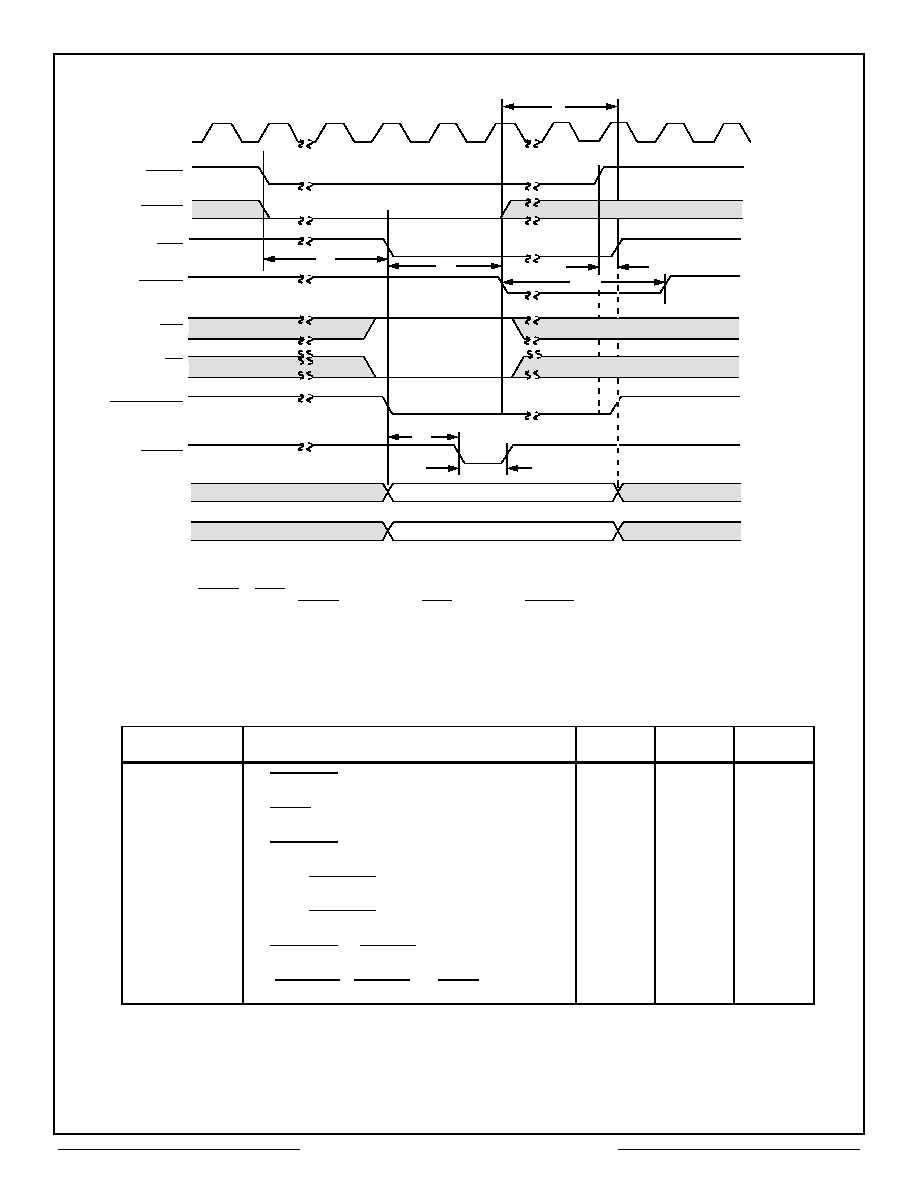
Aeroflex Circuit Technology
28
SCDCT2553 REV B 8/6/99 Plainview NY (516) 694-6700
MEMWR
MEM/REG
A15-A00
IOEN
SELECT
STRBD
(Internal)
16MHz Clock
RD/WR
READYD
See Note 1
td1
tpw1
D15-D00
td2
RAM ADDRESS VALID
td3
RAM DATA VALID
MEMENA-OUT
tpw2
Figure 31 ≠ CPU Writes to RAM Timing
CPU Writes to Ram
SYMBOL
DESCRIPTION
MIN
MAX
UNITS
td1
READYD low delay (CPU Handshake)
-
150
ns
td2
IOEN high delay (CPU Handshake)
-
20
ns
tpw1
READYD pulse width (CPU Handshake)
50
-
ns
td3
CPU MEMWR low delay
-
120
ns
tpw2
CPU MEMWR low pulse width
70
-
ns
tr
READYD to STRBD release
-
1.37
µs
tz
(SELECT
∑
STRBD) to IOEN
-
1.8
µs
NOTE:
1. STRBD to IOEN (low) delay is two clock cycles. If contention occurs, delay is two clock cycles following release of bus.
2. CPU must release STRBD within 1.5µs of IOEN going active. READYD will go away within one clock cycle maximum.
See Note 2
tz
tr
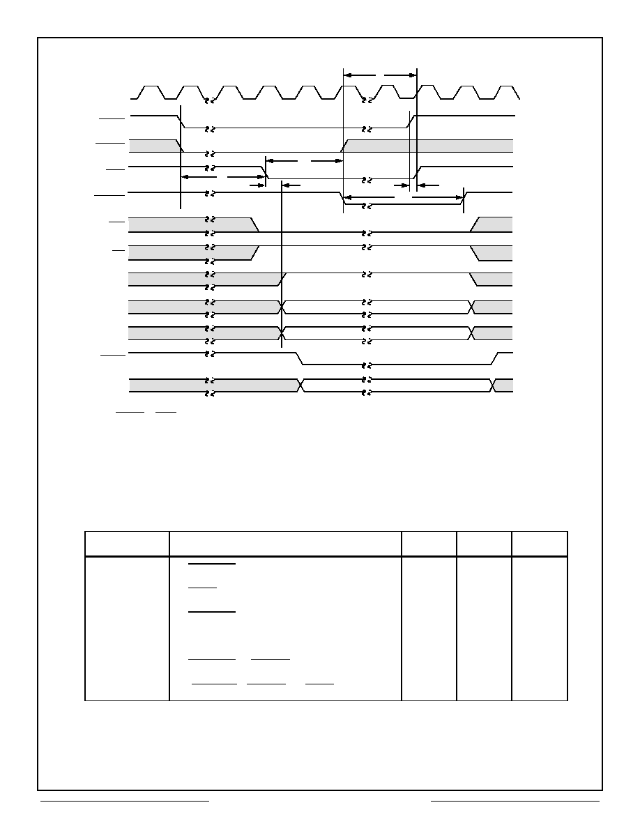
Aeroflex Circuit Technology
29
SCDCT2553 REV B 8/6/99 Plainview NY (516) 694-6700
A02 (38)
A01
A00
MEM/REG
D15-D00
IOEN
SELECT
STRBD
(Internal)
16MHz Clock
RD/WR
READYD
See Note
td1
td8
tpw1
DATA FROM EXTERNAL REGISTER
EXTEN
td2
Figure 32 ≠ CPU Reads from External Register Timing
NOTE: STRBD to IOEN (low) delay is two clock cycles. If contention occurs, delay is two clock cycles following release of bus.
CPU Reads from External Register Timing
SYMBOL
DESCRIPTION
MIN
MAX
UNITS
td1
READYD low delay (CPU Handshake)
-
150
ns
td2
IOEN high delay (CPU Handshake)
-
20
ns
tpw1
READYD pulse width (CPU Handshake)
50
-
ns
td8
Register Data/Address set-up time
-
40
ns
tr
READYD to STRBD release
-
1.37
µs
tz
(SELECT
∑
STRBD) to IOEN
-
1.8
µs
tz
tr
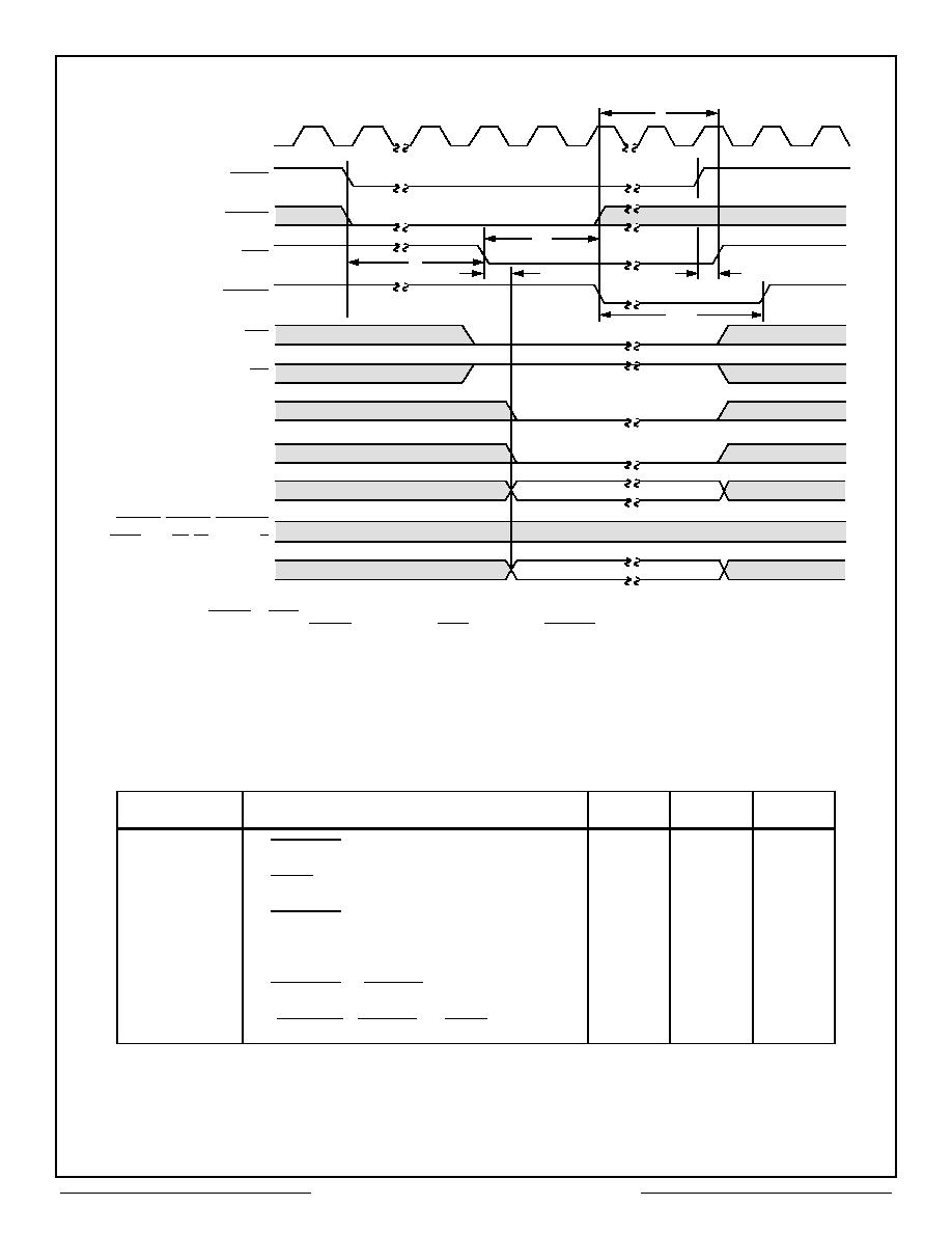
Aeroflex Circuit Technology
30
SCDCT2553 REV B 8/6/99 Plainview NY (516) 694-6700
A02
A01
A00
SSFLAG, SSBUSY, SVCRQST
DBAC, RTU/BC, MT, CTLIN B/A
MEM/REG
D15-D00
IOEN
SELECT
STRBD
(Internal)
16MHz Clock
RD/WR
READYD
See Note 1
DATA VALID
td1
tpw1
td2
td6
Figure 33 ≠ CPU Reads from Internal Register Timing
CPU Reads from Internal Register
SYMBOL
DESCRIPTION
MIN
MAX
UNITS
td1
READYD low delay (CPU Handshake)
-
200
ns
td2
IOEN high delay (CPU Handshake)
-
20
ns
tpw1
READYD pulse width (CPU Handshake)
70
-
ns
td6
Internal Register delay (read)
-
60
ns
tr
READYD to STRBD release
-
1.37
µs
tz
(SELECT
∑
STRBD) to IOEN
-
1.8
µs
See Note 2
tz
tr
NOTE:
1. STRBD to IOEN (low) delay is two clock cycles. If contention occurs, delay is two clock cycles following release of bus.
2. CPU must release STRBD within 1.5µs of IOEN going active. READYD will go away within one clock cycle maximum.
Aeroflex Circuit Technology
31
SCDCT2553 REV B 8/6/99 Plainview NY (516) 694-6700
Table 7A ≠ CT2553 Pin Function Table (78 Pin DIP)
Pin
Name
I
IH
(µA)
I
IL
(mA) I
OH
(µA) I
OL
(mA)
Description
1
D00
(5)
-0.4
-400
3.6
I/O Data Bus Bit 0 (LSB).
2
D02
(5)
-0.4
-400
3.6
I/O Data Bus Bit 2.
3
D04
(5)
-0.4
-400
3.6
I/O Data Bus Bit 4.
4
D06
(5)
-0.4
-400
3.6
I/O Data Bus Bit 6.
5
D08
(5)
-0.4
-400
3.6
I/O Data Bus Bit 8.
6
D10
(5)
-0.4
-400
3.6
I/O Data Bus Bit 10.
7
D12
(5)
-0.4
-400
3.6
I/O Data Bus Bit 12.
8
D14
(5)
-0.4
-400
3.6
I/O Data Bus Bit 14.
9
RTAD1
(5)
-0.4
-
-
Remote Terminal Address Bit 1.
10
RTAD0
(5)
-0.4
-
-
Remote Terminal Address Bit 0 (LSB)
11
RTAD4
(5)
-0.4
-
-
Remote Terminal Address Bit 4 (MSB)
12
ILLCMD
+10
±0.01
-
-
Legal Command. Defines the received command as illegal.
13
SA/MC-0
-
-
-400
2.0
Subaddress/Mode Command Bit 0. Multiplexed output bit-0 of
subaddress/word count field of the current command word. SA/MC
determined by the state of LMC.
14
Logic +5V
-
-
-
-
+5V supply input for digital logic section. B6 counter.
15
SA/MC-1
-
-
-400
2.0
Subaddress/Mode Command Bit 1. In MT mode, pulses every time 32
words have been stored. B7 counter.
16
BCSTRCV
-
-
-400
2.0
Broadcast Received. Indicates current command is a 1553 Broadcast
Command.
17
LMC
-
-
-400
2.0
Latched Mode Command. Logic 1 indicates current command word is a
mode code and selects MC0-MC4. Logic 0 indicates non-mode
comrnand and selects SA0-SA4.
18
-15V
-
-
-
-
-15V input power supply connection for the B channel transceiver.
19
GNDB
-
-
-
-
Ground B. Power supply return connection for the B channel
transceiver.
20
TX/RX-B
-
-
-
-
Transmit/Receive transceiver-B. Input/output to the coupling
transformer that connects to the B channel of the 1553 Bus.
21
Logic GND
-
-
-
-
Logic Ground. Power supply return for the digital logic section.
22
A01
(5)
-0.4
-400
3.6
Address Bit 1
23
A03
(5)
-0.4
-400
3.6
Address Bit 3
24
A05
(5)
-0.4
-400
3.6
Address Bit 5
25
A07
(5)
-0.4
-400
3.6
Address Bit 7
26
A09
(5)
-0.4
-400
3.6
Address Bit 9
27
A11
(5)
-0.4
-400
3.6
Address Bit 11
28
A13
(5)
-0.4
-400
3.6
Address Bit 13
29
A15
(5)
-0.4
-400
3.6
Address Bit 15 (MSB)
30
MEMOE
-400
4.0
Memory Output Enable. A Logic 0 used to enable data output
from memory when
the 1553 or CPU reads from memory.
31
MEMENA-OUT
-
-
-400
4.0
Memory Enable Out. Low level output to enable external RAM.
Used with MEMOE
to read data or with MEMWR to write data into
external RAM.
32
CLOCK IN
±20
±0.02
-
-
Clock Input. 16 MHz TTL clock.
33
MEM/REG
(6)
-0.7
-
-
Memory/Register. Input from CPU to select memory or register data
transfer.
34
STRBD
(6)
-0.7
-
-
Strobe Data. Used in conjunction with SELECT to initiate a data
transfer cycle
to/from CPU.
35
EXTEN
-
-
External Enable. Used to load data into external devices.
36
RD/WR
(6)
-0.7
-
-
Read/Write. Input from the CPU which defines the Data Bus
transfer as a read
or write operation.
37
EXTLD
-
-
External load. Used to load data into external devices.
38
GNDA
-
-
-
-
Ground A. Power supply return connection for the A channel
transceiver.
39
-15VA
-
-
-
-
-I5V input power supply connection for the A channel transceiver.
40
TX/RX-A
-
-
-
-
Transmit/Receive transceiver-A. Input/Output to the coupling
transformer that connects
to the A channel of the 1553 Bus.
41
D01
(5)
-0.4
-400
3.6
I/O Data Bus Bit 1.
42
D03
(5)
-0.4
-400
3.6
I/O Data Bus Bit 3.
43
D05
(5)
-0.4
-400
3.6
I/O Data Bus Bit 5
44
D07
(5)
-0.4
-400
3.6
I/O Data Bus Bit 7.
Aeroflex Circuit Technology
32
SCDCT2553 REV B 8/6/99 Plainview NY (516) 694-6700
45
D09
(5)
-0.4
-400
3.6
I/O Data Bus Bit 9.
46
D11
(5)
-0.4
-400
3.6
I/O Data Bus Bit 11.
47
D13
(5)
-0.4
-400
3.6
I/O Data Bus Bit 13.
48
D15
(5)
-0.4
-400
3.6
I/O Data Bus Bit 15 (MSB).
49
RTAD3
(5)
-0.4
-
-
Remote Terminal Address Bit 3.
50
RTAD2
(5)
-0.4
-
-
Remote Terminal Address Bit 2.
51
RTADP
(5)
-0.4
-
-
Remote Terminal Address Parity input.
52
SA/MC-2
-
-
-400
2.0
Subaddress/Mode Command Bit 2. B8 (MSB) counter.
53
SA/MC-4
-
-
-400
2.0
Subaddress/Mode Command Bit 4.
54
SA/MC-3
-
-
-400
2.0
Subaddress/Mode Command Bit 3.
55
THIS-RT
-
-
-400
2.0
Logic 0 pulse indicates receipt of a valid command word which contains
the Remote Terminal address equivalent to the RTADO-RTAD4 inputs.
56
RTPARERR
-
-
-400
2.0
RTU (address) Parity Error. Logic 0 indicates RTU address parity (odd
parity: RTADO-RTAD4, RTADP) has been violated.
57
T/R
-
-
-400
2.0
Transmit/Receive 1553 data. Latched T/R bit from current command
word.
58
+5VB
-
-
-
-
+5V power supply connection for the B channel transceiver.
59
TX/RX-B
-
-
-
-
Transmit/Receive transceiver-B. Inverted I/O to coupling transformer
that connects to channel B of the 1553 Bus.
60
A00
(5)
-0.4
-400
3.6
Address Bit 0 (LSB).
61
A02
(5)
-0.4
-400
3.6
Address Bit 2.
62
A04
(5)
-0.4
-400
3.6
Address Bit 4.
63
A06
(5)
-0.4
-400
3.6
Address Bit 6.
64
A08
(5)
-0.4
-400
3.6
Address Bit 8.
65
A10
(5)
-0.4
-400
3.6
Address Bit 10.
66
A12
(5)
-0.4
-400
3.6
Address Bit 12.
67
A14
(5)
-0.4
-400
3.6
Address Bit 14.
68
MEMWR
-
-
-400
4.0
Memory Write. Output pulse to write data into memory.
69
MEMENA-IN
±20
±0.02
-
-
Memory Enable In. Enables internal RAM only; connect directly to
MEMENA-OUT.
70
INCMD
-
-
-400
2.0
In Command. Indicates BC or RTU currently in message transfer
sequence.
71
MSTRCLR
(6)
-0.7
-
-
Master Clear. Power-on reset from CPU.
72
INT
-
-
-400
4.0
Interrupt. Interrupt pulse line to CPU.
73
IOEN
-
-
-400
4.0
Input/Output Enable. Output to enable external hybrid to the
address/data bus.
74
SELECT
(6)
-0.7
-
-
Select. Input from the CPU. When active, selects CT2553 for operation.
75
READYD
-
-
-400
4.0
Ready Data. When active indicates data has been received from, or is
available to, the CPU.
76
TAGEN
-
-
-400
4.0
Tag Enable. Enables an external time to counter for transferring the
time tag word into memory.
77
+5VA
-
-
-
-
+5V input/power supply for channel A transceiver.
78
TX/RX-A
-
-
-
-
Transmit/Receive transceiver-A. Inverted I/O to the coupling
transformer that connects
to the A channel of the 1553 Bus.
1. I
IH
is specified at: V
CC
= 5.5V, V
IH
= 2.7V.
2. I
IL
is specified at: V
CC
= 5.5V, V
IL
= 0.4V.
3. I
OH
is specified at: V
CC
= 4.5V, V
IH
= 2.4V.
4. I
OL
is specified at: V
CC
= 4.5V, V
IH
= 0.4V.
5. Internal Pull-up Resistor = 30K Ohms, typ.
6. Internal Pull-up Resistor = 16K Ohms, typ.
7. Pin 13 = B6, Pin 15 = B7 and Pin 52 = B8 (MSB). B6, B7 and B8 are the MSB lines of an 8 BIT Counter used in the BC and MT
mode to count 32 WORD TRANSFERS to memory (16 words received off the bus) for a total of 128 DATA and Tag words (in
MT mode). (See pages 19 & 20 for discussion.)
Table 7A ≠ CT2553 Pin Function Table (78 Pin DIP) (continued)
Pin
Name
I
IH
(µA)
I
IL
(mA) I
OH
(µA) I
OL
(mA)
Description
Aeroflex Circuit Technology
33
SCDCT2553 REV B 8/6/99 Plainview NY (516) 694-6700
21
60
22
61
23
62
24
63
25
64
26
65
27
66
28
67
29
68
30
69
31
70
32
71
33
72
34
73
35
74
36
75
37
76
38
77
39
78
40
1
41
2
42
3
43
4
44
5
45
6
46
7
47
8
48
9
49
10
50
11
51
12
52
13
53
14
54
15
55
16
56
17
57
18
58
19
59
20
D00
D01
D02
D03
D04
D05
D06
D07
D08
D09
D10
D11
D12
D13
D14
D15
RTAD1
RTAD3
RTAD0
RTAD2
RTAD4
RTADP
ILLCMD
SA/MC-2
SA/MC-0
SA/MC-4
LOGIC +5V
SA/MC-3
SA/MC-1
THIS-RT
BCSTRCV
RTPARERR
LMC
T/R
-15VB
+5VB
GNDB
TX/RX-B
TX/RX-B
LOGIC GND
A00
A01
A02
A03
A04
A05
A06
A07
A08
A09
A10
A11
A12
A13
A14
A15
MEMWR
MEMOE
MEMENA-IN
MEMENA-OUT
INCMD
CLOCK IN
MSTRCLR
MEM/REG
INT
STRBD
IOEN
EXTEN
SELECT
RD/WR
READYD
EXTLD
TAGEN
GNDA
+5VA
-15VA
TX/RX-A
TX/RX-A
CT2553
MIL-STD-1553
BUS Controller,
Remote Terminal and
DIP Pin Connection Diagram, CT2553 and Pinout
Table 7B ≠ CT2553 Pin Out Description
(DIP)
Pin
#
Function
Pin
#
Function
1
D00
40
TX/RX-A
2
D02
41
D01
3
D04
42
D03
4
D06
43
D05
5
D08
44
D07
6
D10
45
D09
7
D12
46
D11
8
D14
47
D13
9
RTAD1
48
D15
10
RTAD0
49
RTAD3
11
RTAD4
50
RTAD2
12
ILLCMD
51
RTADP
13
SA/MC-0
52
SA/MC-2
14
LOGIC +5V
53
SA/MC-4
15
SA/MC-1
54
SA/MC-3
16
BCSTRCV
55
THIS-RT
17
LMC
56
RTPARERR
18
-15VB
57
T/R
19
GNDB
58
+5VB
20
TX/RX-B
59
TX/RX-B
21
LOGIC GND
60
A00
22
A01
61
A02
23
A03
62
A04
24
A05
63
A06
25
A07
64
A08
26
A09
65
A10
27
A11
66
A12
28
A13
67
A14
29
A15
68
MEMWR
30
MEMOE
69
MEMENA-IN
31
MEMENA-OUT
70
INCMD
32
CLOCK IN
71
MSTRCLR
33
MEM/REG
72
INT
34
STRBD
73
IOEN
35
EXTEN
74
SELECT
36
RD/WR
75
READYD
37
EXTLD
76
TAGEN
38
GNDA
77
+5VA
39
-15VA
78
TX/RX-A
BUS Monitor
Aeroflex Circuit Technology
34
SCDCT2553 REV B 8/6/99 Plainview NY (516) 694-6700
3
4
5
6
7
8
9
10
11
12
13
14
15
16
17
18
19
20
21
22
23
24
25
26
27
28
29
30
31
32
33
34
35
36
37
38
39
40
41
D00
D01
D02
D03
D04
D05
D06
D07
D08
D09
D10
D11
D12
D13
D14
D15
RTAD1
RTAD3
RTAD0
RTAD2
RTAD4
RTADP
ILLCMD
SA/MC-2
SA/MC-0
SA/MC-4
LOGIC +5V
SA/MC-3
SA/MC-1
THIS-RT
BCSTRCV
RTPARERR
LMC
T/R
-15VB
+5VB
GNDB
TX/RX-B
TX/RX-B
LOGIC GND
A00
A01
A02
A03
A04
A05
A06
A07
A08
A09
A10
A11
A12
A13
A14
A15
MEMWR
MEMOE
MEMENA-IN
MEMENA-OUT
INCMD
CLOCK IN
MSTRCLR
MEM/REG
INT
STRBD
IOEN
EXTEN
SELECT
RD/WR
READYD
EXTLD
TAGEN
GNDA
+5VA
-15VA
TX/RX-A
TX/RX-A
Table 8 ≠ CT2566 Pin Out Description
(FP)
Pin
#
Function
Pin
#
Function
1
N/C
42
N/C
2
D00
43
TX/RX-A
3
D01
44
TX/RX-A
4
D02
45
-15VA
5
D03
46
+5VA
6
D04
47
GNDA
7
D05
48
TAGEN
8
D06
49
EXTLD
9
D07
50
READYD
10
D08
51
RD/WR
11
D09
52
SELECT
12
D10
53
EXTEN
13
D11
54
IOEN
14
D12
55
STRBD
15
D13
56
INT
16
D14
57
MEM/REG
17
D15
58
MSTRCLR
18
RTAD1
59
CLOCK IN
19
RTAD3
60
INCMD
20
RTAD0
61
MEMENA-OUT
21
RTAD2
62
MEMENA-IN
22
RTAD4
63
MEMOE
23
RTADP
64
MEMWR
24
ILLCMD
65
A15
25
SA/MC-2
66
A14
26
SA/MC-0
67
A13
27
SA/MC-4
68
A12
28
LOGIC +5V
69
A11
29
SA/MC-3
70
A10
30
SA/MC-1
71
A09
31
THIS-RT
72
A08
32
BCSTRCV
73
A07
33
RTPARERR
74
A06
34
LMC
75
A05
35
T/R
76
A04
36
-15VB
77
A03
37
+5VB
78
A02
38
GNDB
79
A01
39
TX/RX-B
80
A00
40
TX/RX-B
81
LOGIC GND
41
N/C
82
N/C
Flat Package Pin Connection Diagram, CT2553 and Pinout
1
2
N/C
N/C
N/C
N/C
80
79
78
77
76
75
74
73
72
71
70
69
68
67
66
65
64
63
62
61
60
59
58
57
56
55
54
53
52
51
50
49
48
47
46
45
44
43
42
82
81
CT2553FP
MIL-STD-1553
BUS Controller,
Remote Terminal and
BUS Monitor
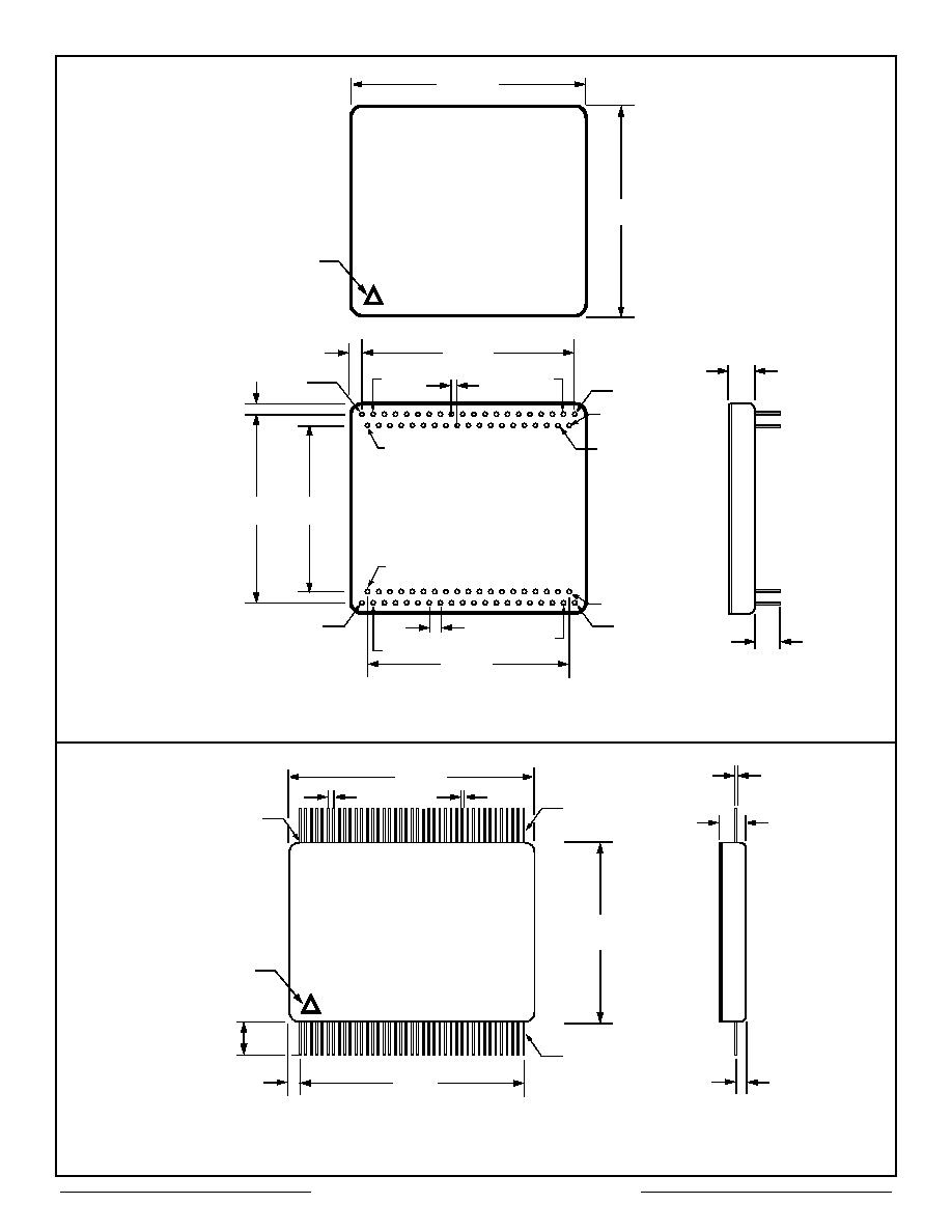
Aeroflex Circuit Technology
35
SCDCT2553 REV B 8/6/99 Plainview NY (516) 694-6700
.100
2.100
1.500
TYP
Lead 1 & ESD
Designator
1.900
1.800
Pin 19
Pin 20
Pin 59
Pin 41
Pin 2
.050
TYP
1.650
1.870
.100
.110
Pin 1
.250
.250
MAX
Pin 39
Pin 40
Pin 78
Pin 22
Pin 21
Pin 60
.018 DIA
TYP
.080
.180
MAX
.010
±.002
.015
2.000
Pin 42
.095
Pin 41
2.200
MAX
Lead 1 & ESD
Designator
1.610
MAX
Designator
MAX
.400
MIN
.050 Lead Centers
41 Leads/Side
(4 Places)
Pin 82
.050
Figure 23 ≠ Plug In Package Outline
Figure 24 ≠ Flat Package Outline
Aeroflex Circuit Technology
36
SCDCT2553 REV B 8/6/99 Plainview NY (516) 694-6700
C I R C U I T T E C H N O L O G Y
Aeroflex Circuit Technology
35 South Service Road
Plainview New York 11803
Telephone: (516) 694-6700
FAX: (516) 694-6715
Toll Free Inquiries: (800) THE-1553
Specifications subject to change without notice
www.aeroflex.com/act1.htm
E-Mail: sales-act@aeroflex.com
Ordering Information
Model Number
Screening
Power Supply
Package
CT2553
Military Temperature, -55∞C to +125∞C,
Screened to the Individual Test Methods
of MIL-STD-883
+5V, -15V
Plug in
CT2553-FP
Flat Package
CT2554
+5V, -12V
Plug in
CT2554-FP
Flat Package
* CT2555
+5V only
Plug in
* CT2555-FP
Flat Package
** CT2556
Plug in
** CT2556-FP
Flat Package
* Contact Factory
** Transceiverless ≠ Contact Factory