MT70014
VLSI COMPONENTS FOR ARINC 429 DATA TRANSMISSION SYSTEMS
1
TWO CHANNEL ARINC TRANSMITTER
∑
8 bit parallel interface
∑
TTL/CMOS compatible I/P
∑
Single 5V supply with low power
consumption
<
50mW
∑
Full MIL operating range
∑
Automatic parity generation
∑
HIGH/LOW speed programmable
independently in each channel

MT70014
VLSI COMPONENTS FOR ARINC 429 DATA TRANSMISSION SYSTEMS
2
MAXIMUM RATINGS
(Above which the useful life may be impaired)
Storage Temperature - 65∫C to +150∫C
Temperature (Ambient) under Bias - 55∫C to +125∫C
Supply Voltage VDD -0.3V to + 7V
DC Input Voltage -0.3 to VDD +0.3V
Output Current (Single O/P) 10mA
Output Current (Total O/P) 20mA
ELECTRICAL CHARACTERISTICS over operating range
PARAMETER
DESCRIPTION
TEST CONDITIONS
MIN
TYP
MAX
UNITS
IOH
Output High Current
VOH=2.8V
VDD=
4.5V
1.0
mA
IOL
Output Low Current
VOL=0.4V
3.2
mA
VIH
Input High Voltage
2.4
VCC
Volts
VIL
Input Low Voltage
-0.3
0.8
Volts
IIL
Input Load Current
VSS
0.45
mA
IOZ
Output Leakage Current
0.4V
<
VO
<
VCC Output Disabled
-40
40
uA
CI
Input Capacitance
Test Frequency = 1.0 MHZ
2
2.6
pF
CI/O
I/O Capacitance
7
9
pF
ICC
Supply Current
VCC = MAX. All inputs
HIGH, All outputs open
.
1.5
mA

MT70014
VLSI COMPONENTS FOR ARINC 429 DATA TRANSMISSION SYSTEMS
3
3.
SWITCHING CHARACTERISTICS (For C
L
= 50pF & RL = 3K ohms)
PARAMETER
Min
Max
Units
f
CLK
Clock Frequency
-
5
MHz
t
P
( Serial data bit period for HNL input high
50/f
uS
(
( Serial data bit period for HNL input low
380/f
uS
(
( (f = f
CLK
/MHz)
t
RES
NRSET pulse width
200nS
-
t
RTC
Propagation delay, NRESET falling edge to TXC high
-
200nS
t
RD
Propagation delay, NRESET falling edge to data outputs low
-
200nS
t
WL
NLD pulse width
200nS
-
t
GL
Gap between NLD pulses
400nS
-
t
SU
Data set up time
100nS
-
t
H
Data hold time
100nS
-
t
LTC
Propagation delay, NLD rising edge following last
-
400nS
byte load to TXZ low
t
R
Output rise time
-
50nS
t
F
Output fall time
-
50nS
t
WTE
NOT Transmit enable pulse width
100nS
-
t
TED
Propagation delay NOT transmit enable falling
)
edge or
)
tp
2tp
NOT Transmission complete falling edge to
)
data output
)
t
DTC
Last data bit of message to TXC high
-
200nS
t
M
Time of data pulse output (mark time)
tp + 1%
2

MT70014
VLSI COMPONENTS FOR ARINC 429 DATA TRANSMISSION SYSTEMS
4
FUNCTIONAL DESCRIPTION
The device consists of two independent channels each of which functions as a parallel to serial data converter.
The parallel data is loaded via an 8-bit input highway and the serial output is generated in the ARINC
format, i.e. 31 bits of data plus one parity bit.
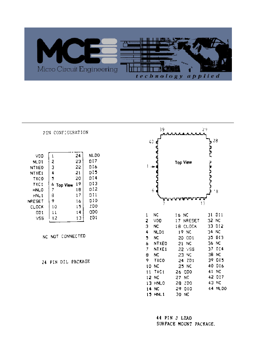
The input highway (DIO to D17) is common to both channels as are the reset (NRESET) CLOCK 9clock),
positive supply (V
DD
), and ground (VSS) pins. Each channel has 3 control inputs. Channel 0 has a `load'
input (NLDO), a `transmit enable' input (NTXEO), and a `high/low speed' (HNLO) control input. There are
3 outputs per channel. Channel 0 has a `data out zeros' (ZDO) output, a `data out ones' (ODO) output and a
`transmission complete' (TXCO) output.
Operations for Channel 0 and Channel 1 are identical in all respects.
The data to be transmitted by a particular channel is loaded as four 8-bit bytes via the input highway. The
four bytes are stored on chip in the order in which they were loaded. Loading is performed by pulsing the
(NLDO) input low. The data must then be changed to the value of the next byte and (NLDO) pulsed low
again etc.
The four bytes are transmitted in the order in which they were loaded. The only exception is the most
significant bit of the 4th byte. This bit is ignored and a parity bit is transmitted in its place. The parity bit
corresponds to an odd parity check on the first 31 bits, i.e. if the number of ones in the first 31 bits is odd, the
parity bit is equal to zero.
Data is only accepted if the TXCO output is high. Once byte 4 has been loaded, TXCO is driven low. Data
must be valid on the input highway for t
su
before and to t
H
after the (NLDO) rising edge.
The clock (CLOCK) input of 5mhz + 1%* is divided down on chip by 50 to give a serial data transmission
rate for (HNLO) high or by 380 for (HNLO) low. These rates correspond to the ARINC fast and slow rates
respectively. The timing of the two output data lines (ODO) and (ZDO) is shown in Fig.2. A data value of
one is signified by a positive pulse output on (ODO) and a zero by a positive pulse on (ZDO). The bit period
tp will be 50/f
CLK
for (HNLO) high and 380/f
CLK
for (HNLO) low.
* ARINC recommends that the transmission rate should not be precisely 100KHZ to avoid interference but
any rate within + 1% of these can be used.
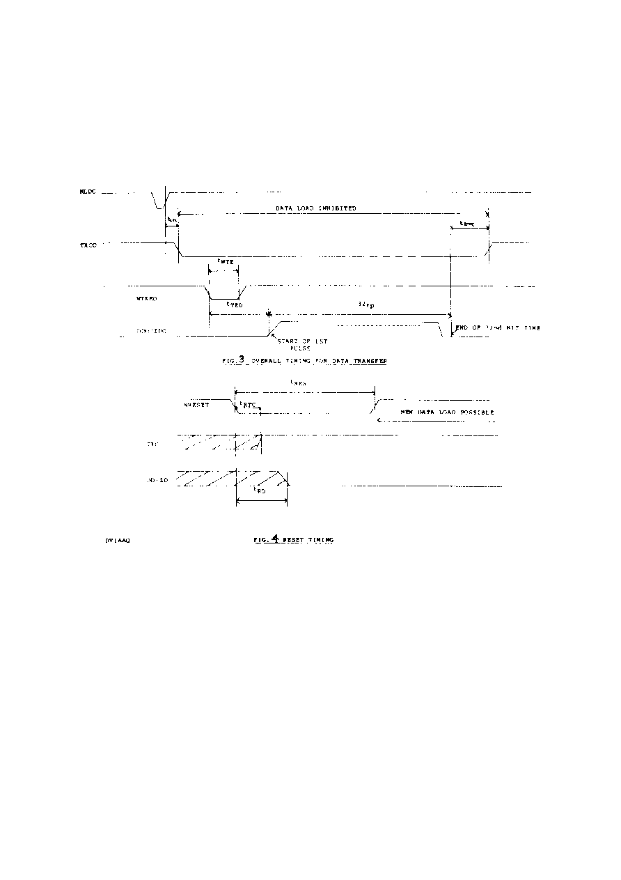
The overall timing diagram for a complete data transfer is shown in Fig.3. When the last byte has been
loaded (TXCO) goes low. This signal is combined with the output of an on chip latch which is set by the
(NTXEO) signal to initiate the start of transmission. The latch is reset upon start of transmission. If the
(NTXEO) signal is left permanently low the on chip latch is always set and transmission will be initiated by
TXCO going low, i.e. as soon as the 4 bytes have been loaded. Hence there is an option between auto-start
and controlled-start of transmission. At the end of the transmission TXCO goes high and the device is able
to accept new data.
The devices can be completely reset by pulsing the (NRESET) line low. This causes both channels to be put
into the data load phase of operation. The TXC lines are forced high and all data outputs are forced low. the
timing is shown in Fig. 4.
INTERFACE DEFINITIONS
The device is implemented as a monolithic circuit using CMOS compatible with standard TLL circuitry.
A circuit with V
OH
(min) = 2.7V and V
OL
(max) = 0.4V will drive all inputs to the device and a standard TTL
circuit with I
IL
(max) = -1.6mA at V
I
= 0.4V and I
IH
(max) = 40 uA at V
I
= 2.4V can be driven by all the
outputs of the device.