FEATURES
q 20MHz 16-bit Microcontroller compatible with Industry
Standard's MCS-96 ISA
- Register to Register Architecture
- 1000 Byte Register RAM
q Three 8-bit I/O Ports
q On-board Interrupt Controller
q Three Pulse-Width Modulated Outputs
q High Speed I/O
q UART Serial Port
q Dedicated Baud Rate Generator
q Software and Hardware Timers
- 16-Bit Watchdog Timer, Four 16-Bit Software Timers
- Three 16-Bit Counter/Timers
q Error detection and correction for external memory accesses
q QML Q compliant part
q Standard Microcircuit Drawing 5962-98583
INTRODUCTION
The UT80C196KD is compatible with industry standard's
MCS-96 instruction set. The UT80C196KD is supported by
commercial hardware and software development tools.
The UT80C196KD accesses instruction code and data via a
16-bit address and data bus. The 16-bit bus allows the
microcontroller to access 128K bytes of instruction/data
memory. Integrated software and hardware timers, high speed
I/O, pulse width modulation circuitry, and UART make the
UT80C196KD ideal for control type applications. The CPU's
ALU supports byte and word adds and subtracts, 8 and 16 bit
multiplies, 32/16 and 16/8 bit divides, as well as increment,
decrement, negate, compare, and logical operations. The
UT80C196KD's interrupt controller prioritizes and vectors 18
interrupt events. Interrupts include normal interrupts and
special interrupts. To reduce power consumption, the
microcontroller supports software invoked idle and power
down modes.
The UT80C196KD is packaged in a 68-lead quad flatpack.
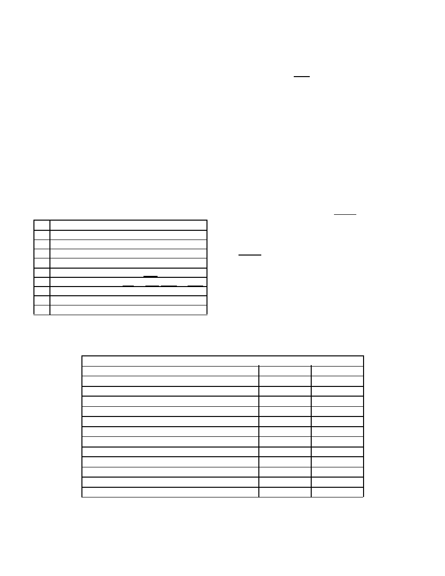
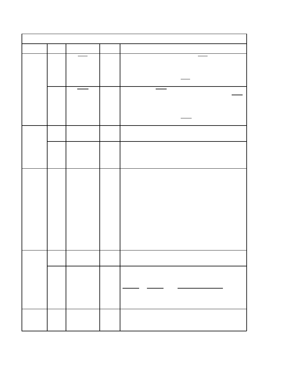
1000 Bytes
RAM
Register File
ALU
MicroCode
Engine
Interrupt
Controller
PTS
Memory
Controller
Queue
Watchdog
Timer
PWM
PORT2
Serial
Port
HSIO and
Timers
HSI HSO
Alternate
Functions
CPU
Alternate
Functions
PORT1
HOLD
HLDA
BREQ
PWM1
PWM2
Control
Signals
Address /Data Bus
Figure 1. UT80C196KD Microcontroller
Fi
rs
tP
as
s
Co
re
IP
PORT0
EXTINT
ECB0-
ECB5
Standard Products
UT80C196KD Microcontroller
Datasheet
September 2002

2
1.0 SIGNAL DESCRIPTION
Port 0 (P0.0 - P0.7): Port 0 is an 8-bit input only port when used
in its default mode. When configured for their alternate function,
five of the bits are bi-directional EDAC check bits as shown in
Table 1.
Port 1 (P1.0 - P1.7): Port 1 is an 8-bit, quasi-bidirectional, I/O
port. All pins are quasi-bidirectional unless the alternate
function is selected per Table 2. When the pins are configured
for their alternate functions, they act as standard I/O, not quasi-
bidirectional.
Port 2 (P2.0 - P2.7): Port 2 is an 8-bit, multifunctional, I/O port.
These pins are shared with timer 2 functions, serial data I/O and
PWM0 output, per Table 3.
AD0-AD7: The lower 8-bits of the multiplexed address/data
bus. The pins on this port are bidirectional during the data phase
of the bus cycle.
AD8-AD15: The upper 8-bits of the multiplexed address/data
bus. The pins on this port are bidirectional during the data phase
of the 16-bit bus cycle. When running in 8-bit bus width, these
pins are non-multiplexed, dedicated upper address bit outputs.
HSI: Inputs to the High Speed Input Unit. Four HSI pins are
available: HSI.0, HSI.1, HSI.2, and HSI.3. Two of these pins
(HSI.2 and HSI.3) are shared with the HSO Unit. Two of these
pins (HSI.0 and HSI.1) have alternate functions for Timer 2.
HSO: Outputs from the High Speed Output Unit. Six HSO pins
are available: HSO.0, HSO.1, HSO.2, HSO.3, HSO.4, and
HSO.5. Pins HSO.4 and HSO.5 are shared with pins HSI.2 and
HSI.3 of the HSI Unit respectively.
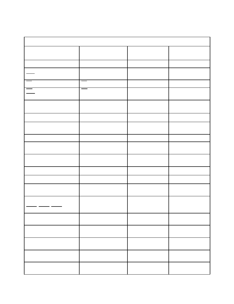
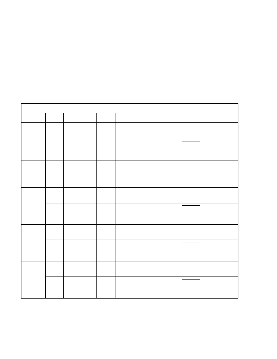
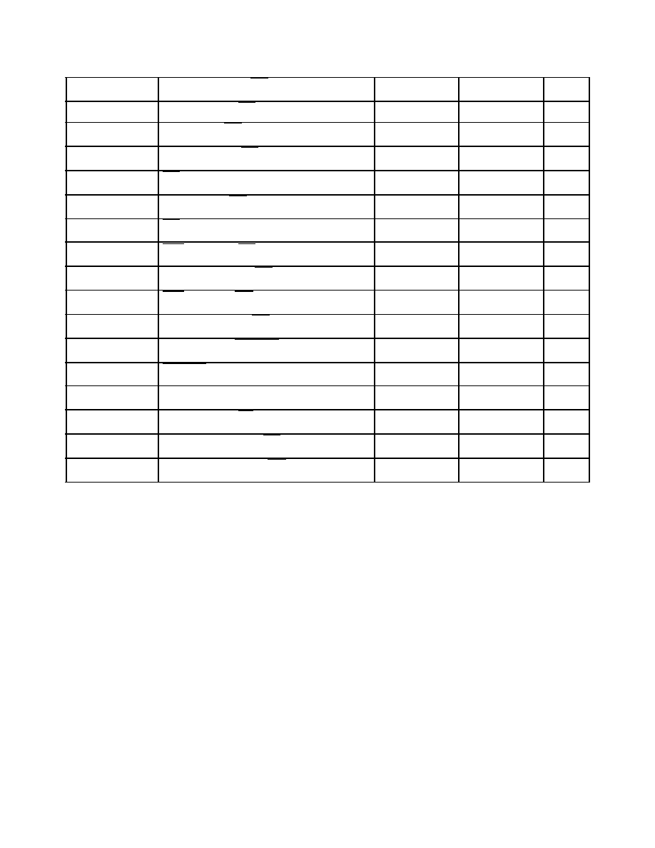
Table 1. Port 0 Alternate Functions
Port Pin
Alternate
Name
Alternate Function
P0.0-P0.3,
P0.6
ECB0-ECB4 Error Detection & Correction
Check Bits
P0.4
P0.5
Input Port Pins
P0.7
EXTINT
Setting IOC1.1=1 will allow P0.7
to be used for EXTINT (INT07)
Table 2. Port 1 Alternate Functions
Port
Pin
Alternate
Name
Alternate Function
P1.0
P1.0
I/O Pin
P1.1
P1.1
I/O Pin
P1.2
P1.2
I/O Pin
P1.3
PWM1
Setting IOC3.2=1 enables P1.3 as
the Pulse Width Modulator
(PWM1) output pin.
P1.4
PWM2
Setting IOC3.3=1 enables P1.4 as
the Pulse Width Modulator
(PWM2) output pin.
P1.5
BREQ
Bus Request, output activated
when the bus controller has a
pending external memory cycle.
P1.6
HLDA
Bus Hold Acknowledge, output
indicating the release of the bus.
P1.7
HOLD
Bus Hold, input requesting control
of the bus.
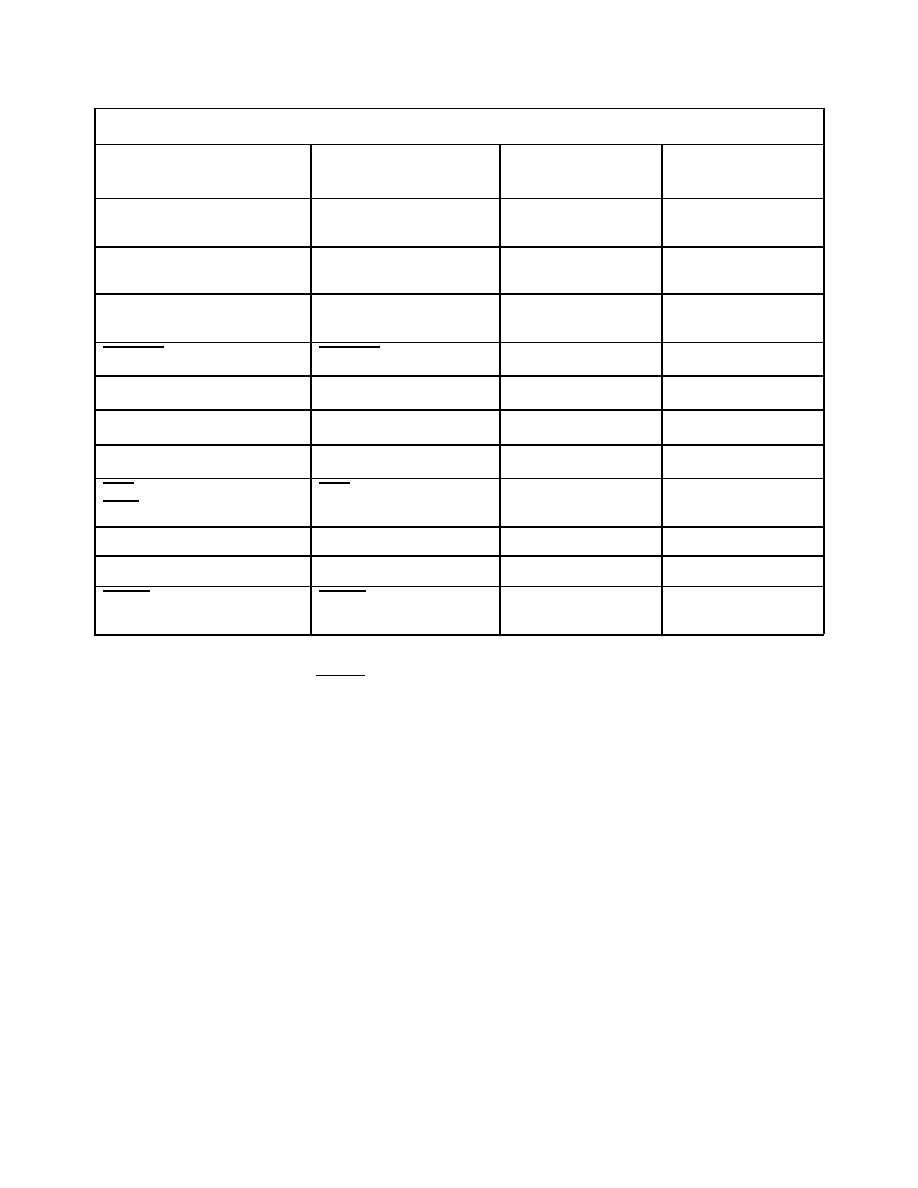
Table 3. Port 2 Alternate Functions
Port
Pin
Alternate
Name
Alternate Function
P2.0
TXD
Transmit Serial Data.
P2.1
RXD
Receive Serial Data.
P2.2
EXTINT
External interrupt. Clearing
IOC1.1 will allow P2.2 to be
used for EXTINT (INT07)
P2.3
T2CLK
Timer 2 clock input and Serial
port baud rate generator input.
P2.4
T2RST
Timer 2 Reset
P2.5
PWM0
Pulse Width Modulator
output 0
P2.6
T2UP-DN
Controls the direction of the
Timer 2 counter. Logic High
equals count down. Logic low
equals count up.
P2.7
T2CAPTURE
A rising edge on P2.7 causes
the value of Timer 2 to be
captured into this register, and
generates a Timer 2 Capture
interrupt (INT11).
3
1.1 Hardware Interface
1.1.1 Interfacing with External Memory
The UT80C196KD can interface with a variety of external
memory devices. It supports either a fixed 8-bit bus width or a
dynamic 8-bit/16-bit bus width, internal READY control for
slow external memory devices, a bus-hold protocol that enables
external devices to take over the bus, and several bus-control
modes. These features provide a great deal of flexibility when
interfacing with external memory devices.
1.1.1.1 Chip Configuration Register
The Chip Configuration Register (CCR) is used to initialize the
UT80C196KD immediately after reset. The CCR is fetched
from external address 2018H (Chip Configuration Byte) after
removal of the reset signal. The Chip Configuration Byte (CCB)
is read as either an 8-bit or 16-bit word depending on the value
of the BUSWIDTH pin. The composition of the bits in the CCR
are shown in Table 4.
There are 8 configuration bits available in the CCR. However,
bits 7 and 6 are not used by the UT80C196KD. Bits 5 and 4
comprise the READY mode control which define internal limits
for waitstates generated by the READY pin. Bit 3 controls the
definition of the ALE/ADV pin for system memory controls
while bit 2 selects between the different write modes. Bit 1
selects whether the UT80C196KD will use a dynamic 16-bit
bus or whether it will be locked in as an 8-bit bus. Finally, Bit
0 enables the Power Down mode and allows the user to disable
this mode for protection against inadvertent power downs.
1.1.1.2 Bus Width and Memory Configurations
The UT80C196KD external bus can operate as either an 8-bit
or 16-bit multiplexed address/data bus (see figure 2). The value
of bit 1 in the CCR determines the bus operation. A logic low
value on CCR.1 locks the bus controller in 8-bit bus mode. If,
however, CCR.1 is a logic high, then the BUSWIDTH signal is
used to decide the width of the bus. The bus is 16 bits wide when
the BUSWIDTH signal is high, and is 8 bits when the
BUSWIDTH signal is low.
1.1.2 Reset
To reset the UT80C196KD, hold the RESET pin low for at least
16 state times after the power supply is within tolerance and the
oscillator has stabilized. Resets following the power-up reset
may be asserted for at least one state time, and the device will
turn on a pull-down transistor for 16 state times. This enables
the RESET signal to function as the system reset. The reset state
of the external I/O is shown in Table 9, and the register reset
values are shown in Table 8.
1.1.3 Instruction Set
The instruction set for the UT80C196KD is compatible with the
industry standard MCS-96 instruction set used on the
80C196KD.
Notes:
1.The first instruction read following reset will be from location 2080h. All other external memory can be used as instruction and/or data memory.
Table 4. Chip Configuration Register
Bit
Function
7
N/A
6
N/A
5
IRC1 - Internal READY Mode Control
4
IRC0 - Internal READY Mode Control
3
Address Valid Strobe Select (ALE/ADV)
2
Write Strobe Mode Select (WR and BHE/WRL and WRH)
1
Dynamic Bus Width Enable
0
Enable Power Down Mode
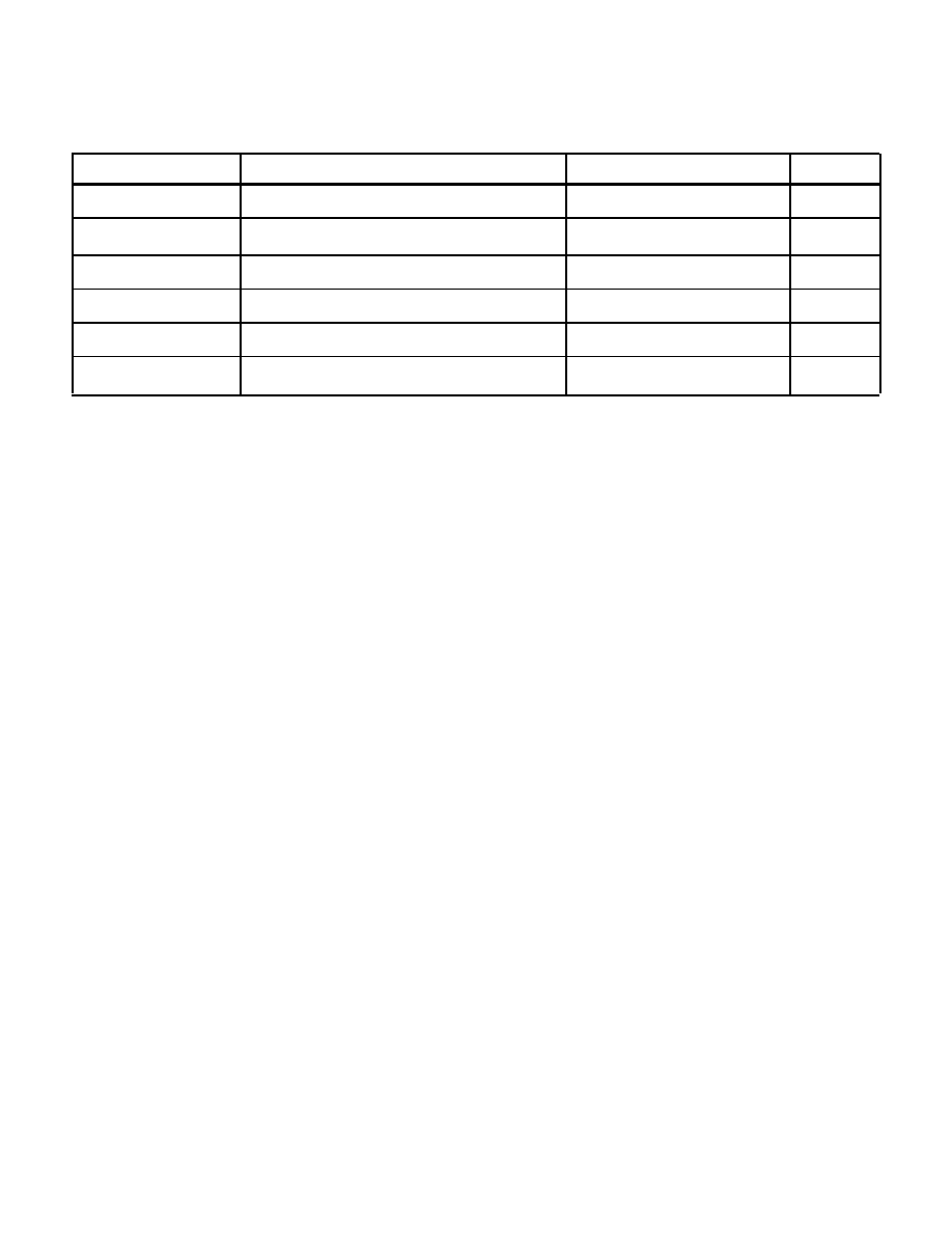
Table 5. Memory Map
Memory Description
Begin
End
External Memory
1
02080H
0FFFFH
Reserved
0205EH
0207FH
PTS Vectors
02040H
0205DH
Upper Interrupt Vectors
02030H
0203FH
Reserved
02020H
0202FH
Reserved
02019H
0201FH
Chip Configuration Byte
02018H
02018H
Reserved
02014H
02017H
Lower Interrupt Vectors
02000H
02013H
External Memory
00400H
1FFFH
Internal Memory (RAM)
0001AH
003FFH
Special Function Registers
00000H
00019H

4
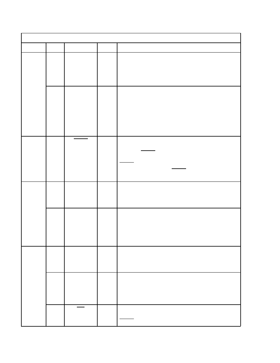
Table 6. Interrupt Vector Sources, Locations, and Priorities
Number
Interrupt Vector
Source(s)
Interrupt
Vector
Location
PTS
Vector
Location
Priority
1
(0 is the
Lowest
Priority)
Special
Unimplemented
Opcode
Unimplemented Opcode
2012h
N/A
N/A
Special
Software Trap
Software Trap
2010h
N/A
N/A
INT 15
NMI
2
NMI
203Eh
N/A
15
INT 14
HSI FIFO Full
HSI FIFO Full
203Ch
205Ch
14
INT 13
EXTINT 1
2
Port 2.2
203Ah
205Ah
13
INT 12
Timer 2 Overflow
Timer 2 Overflow
2038h
2058h
12
INT 11
Timer 2 Capture
2
Timer 2 Capture
2036h
2056h
11
INT 10
HSI FIFO 4
HSI FIFO
Fourth Entry
2034h
2054h
10
INT 9
Receive
RI Flag
3
2032h
2052h
9
INT 8
Transmit
TI Flag
3
2030h
2050h
8
INT 7
EXTINT
2
Port 2.2 or Port 0.7
200Eh
204Eh
7
INT 6
Serial Port
RI Flag and
TI Flag
4
200Ch
204Ch
6
INT 5
Software Timer
Software Timer 0-3
Timer 2 Reset
200Ah
204Ah
5
INT 4
HSI.0
2
HSI.0 Pin
2008h
2048h
4
INT 3
High Speed
Outputs
Events on HSO.0 thru
HSO.5 Lines
2006h
2046h
3
INT 2
HSI Data Available
HSI FIFO Full or
HSI Holding Reg.
Loaded
2004h
2044h
2
INT 1
EDAC Bit Error
Single Bit Error
Single Bit Error OVF
Double Bit Error
2002h
2042h
1
INT 0
Timer Overflow
Timer 1 or Timer 2
2000h
2040h
0
All of the previous maskable interrupts can be assigned to the PTS.
Any PTS interrupt has priority over all other maskable interrupts.

5
Notes:
1.
The Unimplemented Opcode and Software Trap interrupts are not prioritized. The Interrupt Controller immediately services these interrupts when they are
asserted. NMI has the highest priority of all prioritized interrupts. Any PTS interrupt has priority over lower priority intterupts, and over all other maskable
interrupts. The standard maskable interrupts are serviced according to their priority number with INT0 has the lowest priority of all interrupts.
2.
These interrupts can be configured to function as independant, external interrupts.
3.
If the Serial interrupt is masked and the Receive and Transmit interrupts are enabled, the RI flag and TI flag generate separate Receive and Transmit inter-
rupts.
4.
If the Receive and Transmit interrupts are masked and the Serial interrupt is enabled, both RI flag and TI flag generate a Serial Port interrupt.

6
Notes:
1. For some functions that share a register address in HWindow0, the opposite access type (read/write) is available in HWindow 15 if
indicated by the three asterisks (***).
2. These registers are not available in the industry standard 80C196KD. Therefore, industry standard development software will not recognize these
mnemonics, and you will only be able to access them via their physical addresses.
Table 7. SFR Memory Mapping
Address
HWin 0 Read
HWin 0 Write
HWin 1
HWin 15
1
019H
Stack Pntr (hi)
Stack Pntr (hi)
Stack Pntr (hi)
Stack Pntr (hi)
018H
Stack Pntr (lo)
Stack Pntr (lo)
Stack Pntr (lo)
Stack Pntr (lo)
017H
IOS2
PWM0_CTRL
PWM2_CTRL
***
016H
IOS1
IOC1
PWM1_CTRL
***
015H
IOS0
IOC0
EDAC-CS
2
***
014H
WSR
WSR
WSR
WSR
013H
INT_MASK1
INT_MASK1
INT_MASK1
INT_MASK1
012H
INT_PEND1
INT_PEND1
INT_PEND1
INT_PEND1
011H
SP_STAT
SP_CON
RESERVED
***
010H
PORT 2
PORT 2
RESERVED
PSW
2
00FH
PORT 1
PORT 1
Timer 3(hi)
2
RESERVED
00EH
PORT 0
BAUD RATE
Timer 3(lo)
2
RESERVED
00DH
Timer 2 (hi)
Timer 2 (hi)
WDT-SCALE
2
T2CAPTURE (hi)
00CH
Timer 2 (lo)
Timer 2 (lo)
IOC3
T2CAPTURE (lo)
00BH
Timer 1 (hi)
IOC2
INT_PRI(hi)
2
***
00AH
Timer 1 (lo)
Watchdog
INT_PRI(lo)
2
***
009H
INT_PEND
INT_PEND
INT_PEND
INT_PEND
008H
INT_MASK
INT_MASK
INT_MASK
INT_MASK
007H
SBUF (RX)
SBUF (TX)
PTSSRV (hi)
***
006H
HSI_status
HSO_command
PTSSRV (lo)
***
005H
HSI_time(hi)
HSO_time (hi)
PTSSEL (hi)
***
004H
HSI_time (lo)
HSO_time (lo)
PTSSEL (lo)
***
003H
RESERVED
HSI_mode
RESERVED
***
002H
RESERVED
RESERVED
RESERVED
RESERVED
001H
Zero_reg (hi)
Zero_reg (hi)
Zero-reg (hi)
Zero_reg (hi)
000H
Zero_reg (lo)
Zero_reg (lo)
Zero_reg (lo)
Zero_reg (lo)

7
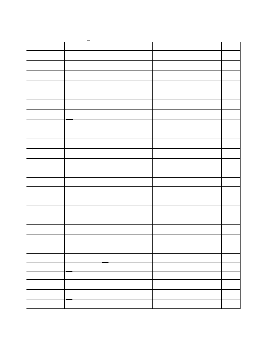
Table 8: Special Function Register Reset Values
Internal Register
Binary Reset State
Hexadecimal Reset
Value
Stack Pointer (SP)
XXXX XXXX XXXX XXXX
XXXX
I/O Status Register 2 (IOS2)
0000 0000
00
I/O Status Register 1 (IOS1)
0000 0000
00
I/O Status Register 0 (IOS0)
0000 0000
00
Window Select Register (WSR)
0000 0000
00
Interrupt Mask Register 1 (INT_MASK1)
0000 0000
00
Interrupt Pending Register 1
(INT_PEND1)
0000 0000
00
Serial Port Status Register (SP_STAT)
0000 1011
0B
Port 2 Register (PORT2)
110X XXX1
XX
Port 1 Register (PORT1)
1111 1111
FF
Port 0 Register (PORT0)
XXXX XXXX
XX
Timer 2 Value Register (TIMER2)
0000 0000 0000 0000
0000
Timer 1 Value Register (TIMER1)
0000 0000 0000 0000
0000
Interrupt Pending Register (INT_PEND)
0000 0000
00
Interrupt Mask Register (INT_MASK)
0000 0000
00
Receive Serial Port Register (SBUF
(RX))
0000 0000
00
HSI Status Register (HSI_status)
X0X0 X0X0
XX
HSI Time Register (HSI_time)
XXXX XXXX XXXX XXXX
XXXX
Zero Register (ZERO_REG)
0000 0000 0000 0000
0000
PWM0 Control Register (PWM0_CTRL)
0000 0000
00
I/O Control Register 1 (IOC1)
0010 0001
21
I/O Control Register 0 (IOC0)
0000 00X0
0X
Serial Port Control Register (SP_CON)
0000 1011
0B
Baud Rate Register (BAUD_RATE)
0000 0000 0000 0001
0001
I/O Control Register 2 (IOC2)
X00X X000
XX
Watch Dog Timer Register (WATCH-
DOG)
0000 0000
00

8
Transmit Serial Port Buffer (SBUF (TX))
0000 0000
00
HSO Command Register
(HSO_command)
0000 0000
00
HSO Time Register (HSO_time)
0000 0000 0000 0000
0000
HSI Mode Register (HSI_mode)
1111 1111
FF
PWM2 Control Register (PWM2_CTRL)
0000 0000
00
PWM1 Control Register (PWM1_CTRL)
0000 0000
00
EDAC Control and Status Register
(EDAC_CS)
0000 0000
00
Timer 3 Value Register (TIMER3)
0000 0000 0000 0000
0000
Watchdog Timer Prescaler
(WDT_SCALE)
0000 0000
00
I/O Control Register 3 (IOC3)
1111 0000
F0
Interrupt Priority Register (INT_PRI)
0000 0000
00
PTS Service Register (PTSSRV)
0000 0000 0000 0000
0000
PTS Select Register (PTSSEL)
0000 0000 0000 0000
0000
Timer 2 Capture Register
(T2CAPTURE)
0000 0000 0000 0000
0000
Program Counter (PC)
0010 0000 1000 0000
2080
Chip Configuration Register (CCR)
XX10 1111
XF
Table 8: Special Function Register Reset Values
Internal Register
Binary Reset State
Hexadecimal Reset
Value
9
Table 9: External I/O Reset State
External I/O
I/O Function After Reset
I/O State During
Reset
I/O State After Reset
Address/Data Bus (AD15:0)
Address/Data Bus
Pulled High
Driven Output
ALE
ADV
ALE
Pulled High
Driven Output
RD
RD
Pulled High
Driven Output
WR
WRL
WR
Pulled High
Driven Output
Port 0 (P0.0-P0.3; P0.6)
ECB(4:0)
[P0.0-P0.3; P0.6] and
ECB(4:0)
Undefined Inputs
1
Undefined I/O
1, 2
Port 0 (P0.4 and P0.5)
P0.4 and P0.5
Undefined Inputs
1
Undefined Inputs
1
Port 0 (P0.7)
EXTINT
P0.7
Undefined Input
1
Undefined Input
1
NMI
NMI
Pulled Down
Pulled Down
HSI.0
T2RST
HSI.0
Disabled Input
1
Disabled Input
1
HSI.1
T2CLK
HSI.1
Disabled Input
1
Disabled Input
1
HSI.2/HSO.4
Undefined
Disabled I/O
1
Disabled I/O
1
HSI.3/HSO.5
Undefined
Disabled I/O
1
Disabled I/O
1
HSO.0 through HSO.3
HSO.0-HSO.3
Pulled Down
Driven Low
Outputs
Port 1 (P1.0-P1.7)
PWM1; PWM2;
BREQ; HLDA; HOLD
P1.0-P1.7
Pulled Up
Pulled Up
Port 2 (P2.0)
TXD
TXD
Pulled Up
Driven High
Output
Port 2 (P2.1)
RXD
RXD
Undefined Input
1
Undefined Input
1
Port 2 (P2.2)
EXTINT
P2.2 and EXTINT
Undefined Input
1
Undefined Input
1
Port 2 (P2.3)
T2CLK
P2.3 and T2CLK
Undefined Input
1
Undefined Input
1
Port 2 (P2.4)
T2RST
P2.4
Undefined Input
1
Undefined Input
1
10
Notes:
1. These pins must not be left floating. Input voltages must not exceed V
DD
during power-up.
2. Do not directly tie these pins to V
DD
or GND; if EDACEN goes low, they may be driven by the UT80C196KD and bus contention may occur.
Port 2 (P2.5)
PWM0
PWM0
Pulled Down
Driven Low Output
Port 2 (P2.6)
T2UP-DN
P2.6
Pulled Up
Pulled Up
Port 2 (P2.7)
T2CAPTURE
P2.7 and T2CAPTURE
Pulled Up
Pulled Up
EDACEN
EDACEN
Undefined Input
1
Undefined Input
1
ECB5
ECB5
Undefined I/O
1
Undefined I/O
1,2
READY
READY
Undefined Input
1
Undefined Input
1
BUSWIDTH
BUSWIDTH
Undefined Input
1
Undefined Input
1
BHE
WRH
BHE
Pulled Up
Driven Output
CLKOUT
CLKOUT
Driven Output
Driven Output
INST
INST
Pulled Down
Driven Output
RESET
RESET
Pulled Low by
System
Pulled Up
Table 9: External I/O Reset State
External I/O
I/O Function After Reset
I/O State During
Reset
I/O State After Reset

11
UT80C196KD
UT80C196KD
Bus Control
16-Bit
Multiplexed
Address/Data
8-Bit
Multiplexed
Address/Data
8-Bit
Latched
Address High
Bus Control
AD0-AD15
AD0-AD7
AD8-AD15
16-Bit Bus
8-Bit Bus
Figure 2. Bus Width Options
12
60
59
58
57
56
55
54
53
52
51
50
49
48
47
46
45
44
2
7
2
8
2
9
3
0
3
1
3
2
3
3
3
4
3
5
3
6
3
7
3
8
3
9
4
0
4
1
4
2
4
3
9
8
7
6
5
4
3
2
1
6
8
6
7
6
6
6
5
6
4
6
3
6
2
6
1
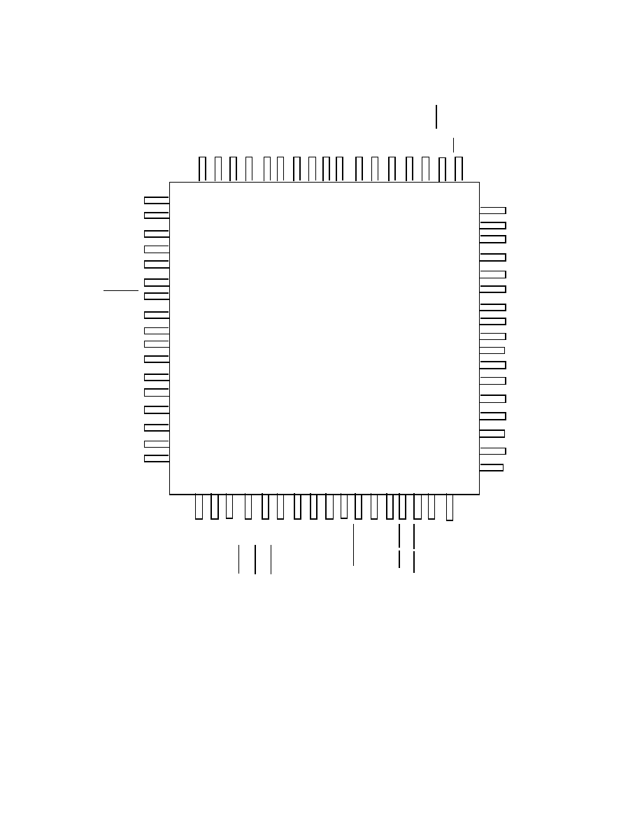
UT80C196KD
TOP VIEW
Figure 3. 68-pin Quad Flatpack Package
AD0
AD1
AD2
AD3
AD4
AD5
AD6
AD7
AD8
AD9
AD10
AD11
AD12
AD13
AD14
AD15
P2.3/T2CLK
H
S
I
.
3
/
H
S
O
.
5
H
S
0
.
0
H
S
0
.
1
B
R
E
Q
/
P
1
.
5
H
L
D
A
/
P
1
.
6
H
O
L
D
/
P
1
.
7
T
2
U
P
-
D
N
/
P
2
.
6
H
S
0
.
2
H
S
0
.
3
V
S
S
E
D
A
C
E
N
T
2
C
A
P
T
U
R
E
/
P
2
.
7
P
W
M
0
/
P
2
.
5
W
R
/
W
R
L
B
H
E
/
W
R
H
T
2
R
S
T
/
P
2
.
4
R
E
A
D
Y
P
0
.
7
/
E
X
T
I
N
T
P
0
.
6
/
E
C
B
0
P
0
.
2
/
E
C
B
1
P
0
.
0
/
E
C
B
2
P
0
.
1
/
E
C
B
3
P
0
.
3
/
E
C
B
4
N
M
I
E
C
B
5
V
D
D
V
S
S
X
T
A
L
1
V
S
S
C
L
K
O
U
T
B
U
S
W
I
D
T
H
I
N
S
T
A
L
E
/
A
D
V
R
D
10
11
12
13
14
15
16
17
18
19
20
21
22
23
24
25
26
P0.5
P0.4
V
SS
V
DD
V
SS
EXTINT/P2.2
RESET
RXD/P2.1
TXD/P2.0
P1.0
P1.1
P1.2
PWM1/P1.3
PWM2/P1.4
T2RST/HSI.0
T2CLK/HSI.1
HSI.2/HS0.4
13
Legend for I/O fields:
TO
= TTL compatible output
TI
= TTL compatible input
CI
= CMOS only input
TUO
= TTL compatible output
(internally pulled high)
TDO
= TTL compatible output
(internally pulled low)
TUI
= TTL compatible input
(internally pulled high)
TDI
= TTL compatible input
(internally pulled low)
TB
= TTL compatible bidirectional
TUQ
= TTL compatible quasi-bidirectional
(internally pulled high)
TUB
= TTL compatible bidirectional
(internally pulled high)
TUBS
= TTL compatible bidirectional Schmitt
Trigger (internally pulled high)
PWR = +5V (V
DD
)
GND = OV (V
SS
)
Table 10: 68-lead Flat Pack Pin Descriptions
QFP Pin#
I/O
Name
Active
Description
1
PWR
V
DD
---
Digital supply voltage (+5V). There are 2 V
DD
pins, both of
which must be connected.
2
TB
ECB5
1
---
EDAC Check Bit 5. Asserting the EDACEN pin will cause the
error detection and correction engine to pass the EDAC Check
Bit 5 through pin 2 of the UT80C196KD.
3
TDI
NMI
High
Non-Maskable Interrupt. A positive transition causes a vector
through the NMI interrupt at location 203Eh. Assert NMI for at
least 1 state time to guarantee acknowledgment by the interrupt
controller.
4
TI
P0.3
---
Port 0 Pin 3. An input only port pin that is read at location 0Eh
in HWindow 0.
TB
ECB4
1
---
EDAC Check Bit 4. Asserting the EDACEN pin will cause the
error detection and correction engine to pass the EDAC Check
Bit 4 through pin 4 of the UT80C196KD.
5
TI
P0.1
---
Port 0 Pin 1. An input only port pin that is read at location 0Eh
in HWindow 0.
TB
ECB3
1
---
EDAC Check Bit 3. Asserting the EDACEN pin will cause the
error detection and correction engine to pass the EDAC Check
Bit 3 through pin 5 of the UT80C196KD.
6
TI
P0.0
---
Port 0 Pin 0. An input only port pin that is read at location 0Eh
in HWindow 0.
TB
ECB2
1
---
EDAC Check Bit 2. Asserting the EDACEN pin will cause the
error detection and correction engine to pass the EDAC Check
Bit 2 through pin 6 of the UT80C196KD.
14
7
TI
P0.2
---
Port 0 Pin 2. An input only port pin that is read at location 0Eh
in HWindow 0.
TB
ECB1
1
---
EDAC Check Bit 1. Asserting the EDACEN pin will cause the
error detection and correction engine to pass the EDAC Check
Bit 1 through pin 7 of the UT80C196KD.
8
TI
P0.6
---
Port 0 Pin 6. An input only port pin that is read at location 0Eh
in HWindow 0.
TB
ECB0
1
---
EDAC Check Bit 0. Asserting the EDACEN pin will cause the
error detection and correction engine to pass the EDAC Check
Bit 0 through pin 8 of the UT80C196KD.
9
TI
P0.7
---
Port 0 Pin 7. An input only port pin that is read at location 0Eh
in HWindow 0.
TI
EXTINT
High
External Interrupt. Setting IOC1.1 = 1 enables pin 9 as the
source for the external interrupt EXTINT. A rising edge on this
pin will generate EXTINT (INT07, 200Eh). Assert EXTINT for
at least 2 state times to ensure acknowledgment by the interrupt
controller.
During Power Down mode, asserting EXTINT places the chip
back into normal operation, even if EXTINT is masked.
10
TI
P0.5
---
Port 0 Pin 5. An input only port pin that is read at location 0Eh
in HWindow 0.
11
TI
P0.4
---
Port 0 Pin 4. An input only port pin that is read at location 0Eh
in HWindow 0.
12
GND
V
SS
---
Digital circuit ground (0V). There are 4 V
SS
pins, all of which
must be connected and one additional recommeded V
SS
connec-
tion.
13
PWR
V
DD
---
Digital supply voltage (+5V). There are 2 V
DD
pins, both of
which must be connected.
14
GND
V
SS
---
Digital circuit ground (0V). There are 4 V
SS
pins, all of which
must be connected and one additional recommeded V
SS
connec-
tion.
Table 10: 68-lead Flat Pack Pin Descriptions
QFP Pin#
I/O
Name
Active
Description
15
15
TI
P2.2
---
Port 2 Pin 2. An input only port pin that is written at location
10h of HWindow 0. P2.2 will always generate EXTINT1
(INT13, 203Ah) unless masked by the INT_MASK1 register.
Assert EXTINT1 for at least 2 state times to guarantee acknowl-
edgment by the interrupt controller.
TI
EXTINT
High
External Interrupt. Setting IOC1.1 = 0 enables pin 15 as the
source for the external interrupt EXTINT. A rising edge on this
pin will generate EXTINT (INT07, 200Eh). Assert EXTINT for
at least 2 state times to ensure acknowledgment by the interrupt
controller.
During Power Down mode, asserting EXTINT places the chip
back into normal operation, even if EXTINT is masked.
16
TUBS
RESET
Low
Master Reset. The first external reset signal supplied to the
UT80C196KD must be active for at least 16 state times. All
subsequent RESET assertions need only be active for 1 state
time because the UT80C196KD will continue driving the
RESET signal for an additional 16 state times. See section 1.1.2
for more information on the RESET function of the
UT80C196KD.
17
TI
P2.1
---
Port 2 Pin 1. An input only port pin that is read at location 10h
of HWindow 0.
Setting SPCON.3 = 0 enables the P2.1 function of pin 17.
TB
RXD
---
RXD is a bidirectional serial data port. When operating in Serial
Modes 1, 2, and 3, RXD receives serial data. When using Serial
Mode 0, RXD operates as an input and an open-drain output for
data.
Setting SPCON.3 = 1 enables the RXD function of pin 17.
18
2
TUO
P2.0
---
Port 2 Pin 0. An output only port pin that is written at location
10h of HWindow 0.
Setting IOC1.5 = 0 enables the P2.0 function of pin 18.
TUO
TXD
---
Transmit Serial Data (TXD). When set to Serial Mode 1, 2, or 3,
TXD transmits serial port data. When using Serial Mode 0,
TXD is used as the Serial Clock output.
Setting IOC1.5 = 1 enables the TXD function of pin 18.
TUI
ICT
Low
In-Circuit Test. The UT80C196KD will enter the In-Circuit
Test mode if this pin is held low during the rising edge of
RESET.
Table 10: 68-lead Flat Pack Pin Descriptions
QFP Pin#
I/O
Name
Active
Description

16
19
TUQ
P1.0
---
Port 1 Pin 0. A quasi-bidirectional port pin that is read and writ-
ten at location 0Fh of HWindow 0.
20
TUQ
P1.1
---
Port 1 Pin 1. A quasi-bidirectional port pin that is read and writ-
ten at location 0Fh of HWindow 0.
21
TUQ
P1.2
---
Port 1 Pin 2. A quasi-bidirectional port pin that is read and writ-
ten at location 0Fh of HWindow 0.
22
TUQ
P1.3
---
Port 1 Pin 3. A quasi-bidirectional port pin that is read and writ-
ten at location 0Fh of HWindow 0.
Setting IOC3.2 = 0 enables the P1.3 function of pin 22.
TUO
PWM1
---
Pulse Width Modulator (PWM) Output 1. The output signal
will be a waveform whose duty cycle is programmed by the
PWM1_CONTROL register, and the frequency is selected by
IOC2.2.
Setting IOC3.2 = 1 enables the PWM1 function of pin 22.
23
TUQ
P1.4
---
Port 1 Pin 4. A quasi-bidirectional port pin that is read and writ-
ten at location 0Fh of HWindow 0.
Setting IOC3.3 = 0 enables the P1.4 function of pin 23.
TUO
PWM2
---
Pulse Width Modulator (PWM) Output 2. The output signal
will be a waveform whose duty cycle is programmed by the
PWM2_CONTROL register, and the frequency is selected by
IOC2.2.
Setting IOC3.3 = 1 enables the PWM2 function of pin 23.
24
TI
HSI.0
---
High Speed Input Module, input pin 0. Unless masked, a rising
edge on this input will generate the HSI.0 Pin interrupt (INT04,
2008h). Assert the HSI.0 pin for at least 2 state times to ensure
acknowledgment by the interrupt controller.
Setting IOC0.0 = 1 enables pin 24 as an HSI input, and allows
events on this pin to be loaded into the HSI FIFO.
TI
T2RST
High
Timer 2 Reset. A rising edge on the T2RST pin resets Timer 2.
To enable the T2RST function of pin 24, set IOC0.3 = 1 and
IOC0.5 = 1.
Table 10: 68-lead Flat Pack Pin Descriptions
QFP Pin#
I/O
Name
Active
Description

17
25
TI
HSI.1
---
High Speed Input Module, input pin 1.
Setting IOC0.2 = 1 enables pin 25 as an HSI input, and allows
events on this pin to be loaded into the HSI FIFO.
TI
T2CLK
---
Timer 2 Clock.
Setting IOC0.7 = 1 and IOC3.0 = 0 enables pin 25 to function as
the Timer 2 clock source.
26
TO
HSO.4
---
High Speed Output Module, output pin 4. This pin can simulta-
neously operate in the HSI and HSO modes of operation. As a
result, this pin acts as an output that the HSI monitors.
Setting IOC1.4 = 1 enables the HSO.4 function of pin 26.
TI
HSI.2
---
High Speed Input Module, input pin 2. This pin can simulta-
neously operate in the HSI and HSO modes of operation. As a
result, this pin can monitor events on the HSO.
Setting IOC0.4 = 1 enables pin 26 as an HSI input pin, and
allows events on this pin to be loaded into the HSI FIFO.
27
TO
HSO.5
---
High Speed Output Module, output pin 5. This pin can simulta-
neously operate in the HSI and HSO modes of operation. As a
result, this pin acts as an output that the HSI monitors.
Setting IOC1.6 = 1 enables the HSO.5 function of pin 27.
TI
HSI.3
---
High Speed Input Module, input pin 3. This pin can simulta-
neously operate in the HSI and HSO modes of operation. As a
result, this pin can monitor events on the HSO.
Setting IOC0.6 = 1 enables pin 27 as an HSI input pin, and
allows events on this pin to be loaded into the HSI FIFO.
28
TDO
HSO.0
---
High Speed Output Module, output pin 0. The HSO.0 pin is a
dedicated output for the HSO module.
29
TDO
HSO.1
---
High Speed Output Module, output pin 1. The HSO.1 pin is a
dedicated output for the HSO module.
Table 10: 68-lead Flat Pack Pin Descriptions
QFP Pin#
I/O
Name
Active
Description

18
30
TUQ
P1.5
---
Port 1 Pin 5. A quasi-bidirectional port pin that is read and writ-
ten at location 0Fh of HWindow 0.
Setting WSR.7 = 0 enables the P1.5 function of pin 30.
TUO
BREQ
Low
Bus Request. The BREQ output signal asserts during a HOLD
cycle when the internal bus controller has a pending external
memory cycle.
During a HOLD cycle, BREQ will not be asserted until the
HLDA signal is asserted. Once asserted, BREQ does not deas-
sert until the HOLD signal is released.
Setting WSR.7 = 1 enables the BREQ function of pin 30.
31
2
TUQ
P1.6
---
Port 1 Pin 6. A quasi-bidirectional port pin that is read and writ-
ten at location 0Fh of HWindow 0.
Setting WSR.7 = 0 enables the P1.6 function of pin 31.
TUO
HLDA
Low
Bus Hold Acknowledge. The UT80C196KD asserts the HLDA
signal as a result of another device activating the HOLD signal.
By asserting this signal, the UT80C196KD is indicating that it
has released the bus.
Setting WSR.7 = 1 enables the HLDA function of pin 31.
32
TUQ
P1.7
---
Port 1 Pin 7. A quasi-bidirectional port pin that is read and writ-
ten at location 0Fh of HWindow 0.
Setting WSR.7 = 0 enables the P1.7 function of pin 32.
TUI
HOLD
Low
Bus Hold. The HOLD signal is used to request control of the
bus by another DMA device.
Setting WSR.7 = 1 enables the HOLD function of pin 32.
33
TUQ
P2.6
---
Port 2 Pin 6. A quasi-bidirectional port pin that is read and writ-
ten at location 10h of HWindow 0.
Setting IOC2.1 = 0 enables the P2.6 function of pin 33.
TUI
T2UP-DN
---
Timer 2 Up or Down. The T2UP-DN pin will dynamically
change the direction that Timer 2 counts.
T2UP-DN = 1 then Timer 2 counts down.
T2UP-DN = 0 then Timer 2 counts up.
Setting IOC2.1 = 1 enables the T2UP-DN function of pin 33.
When IOC2.1 = 0, Timer 2 will only count up.
Table 10: 68-lead Flat Pack Pin Descriptions
QFP Pin#
I/O
Name
Active
Description

19
34
TDO
HSO.2
---
High Speed Output Module, output pin 2. The HSO.2 pin is a
dedicated output for the HSO module.
35
TDO
HSO.3
---
High Speed Output Module, output pin 3. The HSO.3 pin is a
dedicated output for the HSO module.
36
GND
V
SS
---
Digital circuit ground (0V). There are 4 V
SS
pins, all of which
must be connected and one additional recommeded V
SS
connec-
tion.
37
TI
EDACEN
Low
EDAC Enable. Asserting the EDACEN signal activates the
error detection and correction engine. This causes the
UT80C196KD to include ECB(5:0) as the EDAC check bit pins
in all external memory cycles.
38
TUQ
P2.7
---
Port 2 Pin 7. A quasi-bidirectional port pin that is read and writ-
ten at location 10h of HWindow 0.
TUQ
T2CAPTURE
High
Timer 2 Capture. A rising edge on this pin loads the value of
Timer 2 into the T2CAPTURE register, and generates a Timer 2
Capture interrupt (INT11, 2036h). Assert the T2CAPTURE sig-
nal for at least 2 state times to guarantee acknowledgment by the
interrupt controller. Using INT_Mask1.3 controls whether or not
a rising edge causes an interrupt.
39
TDO
P2.5
---
Port 2 Pin 5. An output only port pin that is written at location
10h of HWindow 0.
Setting IOC1.0 = 0 enables the P2.5 function of pin 39.
TDO
PWM0
---
Pulse Width Modulator (PWM) Output 0. The output signal
will be a waveform whose duty cycle is programmed by the
PWM0_CONTROL register, and the frequency is selected by
IOC2.2.
Setting IOC1.0 = 1 enables the PWM0 function of pin 39.
40
2
TUO
WR
Low
Write. The WR signal indicates that an external write is occur-
ring. Activation of this signal only occurs during external mem-
ory writes.
Setting CCR.2 = 1 enables the WR function of pin 40.
TUO
WRL
Low
Write Low. The WRL signal is activated when writing the low
byte of a 16-bit wide word, and is always asserted for 8-bit wide
memory writes.
Setting CCR.2 = 0 enables the WRL function of pin 40.
Table 10: 68-lead Flat Pack Pin Descriptions
QFP Pin#
I/O
Name
Active
Description
20
41
TUO
BHE
Low
Byte High Enable. The assertion of the BHE signal will occur
for all 16-bit word writes, and high byte writes in both 8- and 16-
bit wide bus cycles.
Setting CCR.2 = 1 enables the BHE function of pin 41.
TUO
WRH
Low
Write High. The WRH signal is asserted for high byte writes,
and word writes for 16-bit wide bus cycles. Additionally, WRH
is asserted for all write operations when using an 8-bit wide bus
cycle.
Setting CCR.2 = 0 enables the WRH function of pin 41.
42
TI
P2.4
---
Port 2 Pin 4. An input only port pin that is read at location 10h
of HWindow 0.
TI
T2RST
High
Timer 2 Reset. Asserting the T2RST signal will reset Timer 2.
To enable the T2RST function of pin 42, set IOC0.3 = 1 and
IOC0.5 = 0.
43
TI
READY
High
READY input. The READY signal is used to lengthen memory
cycles by inserting "wait states" for interfacing to slow peripher-
als. When the READY signal is high, no "wait states" are gener-
ated, and the CPU operation continues in a normal fashion. If
READY is low during the falling edge of CLKOUT, the mem-
ory controller inserts "wait states" into the memory cycle. "Wait
state" generation will continue until a falling edge of CLKOUT
detects READY as logically high, or until the number of "wait
states" is equal to the number programmed into CCR.4 and
CCR.5.
Note: The READY signal is only used for external memory
accesses, and is functional during the CCR fetch.
44
TI
P2.3
---
Port 2 Pin 3. An input only port pin that is read at location 10h
of HWindow 0.
TI
T2CLK
---
Timer 2 Clock input. Setting IOC0.7 = 0 and IOC3.0 = 0
enables this pin as the external clock source for Timer 2.
IOC0.7: IOC3.0: Timer 2 Clock Source:
X 1 Internal Clock Source
0 0 P2.3 External Clock Source
1 0 HSI.1 External Clock Source
45
TUB
AD15
---
Bit 15 of the Address/Data bus. This pin is a dedicated address
pin when operating with 8-bit wide bus cycles. For 16-bit wide
bus cycles, this pin is used as multiplexed address and data.
Table 10: 68-lead Flat Pack Pin Descriptions
QFP Pin#
I/O
Name
Active
Description

21
46
TUB
AD14
---
Bit 14 of the Address/Data bus. This pin is a dedicated address
pin when operating with 8-bit wide bus cycles. For 16-bit wide
bus cycles, this pin is used as multiplexed address and data.
47
TUB
AD13
---
Bit 13 of the Address/Data bus. This pin is a dedicated address
pin when operating with 8-bit wide bus cycles. For 16-bit wide
bus cycles, this pin is used as multiplexed address and data.
48
TUB
AD12
---
Bit 12 of the Address/Data bus. This pin is a dedicated address
pin when operating with 8-bit wide bus cycles. For 16-bit wide
bus cycles, this pin is used as multiplexed address and data.
49
TUB
AD11
---
Bit 11 of the Address/Data bus. This pin is a dedicated address
pin when operating with 8-bit wide bus cycles. For 16-bit wide
bus cycles, this pin is used as multiplexed address and data.
50
TUB
AD10
---
Bit 10 of the Address/Data bus. This pin is a dedicated address
pin when operating with 8-bit wide bus cycles. For 16-bit wide
bus cycles, this pin is used as multiplexed address and data.
51
TUB
AD9
---
Bit 9 of the Address/Data bus. This pin is a dedicated address
pin when operating with 8-bit wide bus cycles. For 16-bit wide
bus cycles, this pin is used as multiplexed address and data.
52
TUB
AD8
---
Bit 8 of the Address/Data bus. This pin is a dedicated address
pin when operating with 8-bit wide bus cycles. For 16-bit wide
bus cycles, this pin is used as multiplexed address and data.
53
TUB
AD7
---
Bit 7 of the Address/Data bus. This pin is used as multiplexed
address and data for both 8- and 16-bit wide bus cycles.
54
TUB
AD6
---
Bit 6 of the Address/Data bus. This pin is used as multiplexed
address and data for both 8- and 16-bit wide bus cycles.
55
TUB
AD5
---
Bit 5 of the Address/Data bus. This pin is used as multiplexed
address and data for both 8- and 16-bit wide bus cycles.
56
TUB
AD4
---
Bit 4 of the Address/Data bus. This pin is used as multiplexed
address and data for both 8- and 16-bit wide bus cycles.
57
TUB
AD3
---
Bit 3 of the Address/Data bus. This pin is used as multiplexed
address and data for both 8- and 16-bit wide bus cycles.
58
TUB
AD2
---
Bit 2 of the Address/Data bus. This pin is used as multiplexed
address and data for both 8- and 16-bit wide bus cycles.
59
TUB
AD1
---
Bit 1 of the Address/Data bus. This pin is used as multiplexed
address and data for both 8- and 16-bit wide bus cycles.
60
TUB
AD0
---
Bit 0 of the Address/Data bus. This pin is used as multiplexed
address and data for both 8- and 16-bit wide bus cycles.
Table 10: 68-lead Flat Pack Pin Descriptions
QFP Pin#
I/O
Name
Active
Description

22
Notes:
1. These pins should be pulled high or low when using EDAC (i.e. EDACEN = 0) to prevent the voltages on these pins from floating to the switching threshold of
the input buffers during long read cycles.
2. These pins must be high on the rising edge of RESET in order to avoid entering any test modes.
3. This pin is a recommended V
SS
connection. The remaining 4 V
SS
pins are required to be tied to the circuit card ground plane.
61
2
TUO
RD
Low
Read. The RD signal is an output to external memory that is
only asserted during external memory reads.
62
2
TUO
ALE
High
Address Latch Enable. The ALE signal is an output to external
memory that is only asserted during external memory accesses.
ALE is used to specify that valid address information is avail-
able on the address/data bus, and signals the start of a bus cycle.
ALE is used by an external latch to demultiplex the address from
the address/data bus. Setting CCR.3 = 1 enables the ALE func-
tion of pin 62.
TUO
ADV
Low
Address Valid. The ADV signal is an output to external mem-
ory that is only asserted during external memory accesses. ADV
is driven high to specify that valid address information is avail-
able on the address/data bus. The ADV signal is held low during
the data transfer portion of the bus cycle, and is driven high
when the bus cycle completes. ADV is used by an external latch
to demultiplex the address from the address/data bus. Setting
CCR.3 = 0 enables the ADV function of pin 62.
63
TDO
INST
High
Instruction Fetch. The INST signal indicates the type of external
memory cycle being performed. The INST signal will be high
during instruction fetches, and will be low for data fetches.
Note: CCB bytes and Interrupt vectors are considered data.
64
TI
BUSWIDTH
---
Bus Width. The BUSWIDTH pin dynamically modifies the
width of bus cycles. When a high logic value is supplied, the
bus width will be set to 16-bits wide. When a low logic level is
supplied, the bus width will be set to 8-bits wide.
Setting CCR.1 = 1 enables the BUSWIDTH pin. Setting
CCR.1 = 0 disables the BUSWIDTH pin. As a result, the
UT80C196KD will only perform 8-bit wide bus cycles.
65
TUO
CLKOUT
---
Clock Output. The CLKOUT signal is the output of the internal
clock. This signal has a 50% duty cycle, and runs at 1/2 the fre-
quency of the system clock input to XTAL1. Setting IOC3.1 = 0
will enable the CLKOUT output signal.
66
GND
V
SS
3
---
Digital circuit ground (0V). Recommended connection for sig-
nal integrity improvement. There are 4 V
SS
pins, all of which
must be connected.
67
CI
XTAL1
---
External oscillator or clock input to the UT80C196KD. The
XTAL1 input is fed to the on-chip clock generator.
68
GND
V
SS
---
Digital circuit ground (0V). There are 4 V
SS
pins, all of which
must be connected and one additional recommeded V
SS
connec-
tion.
Table 10: 68-lead Flat Pack Pin Descriptions
QFP Pin#
I/O
Name
Active
Description
23
2.0 ABSOLUTE MAXIMUM RATINGS
1
(Referenced to V
SS
)
Notes:
1. Stresses outside the listed absolute maximum ratings may cause permanent damage to the device. This is a stress rating only, and functional operation of the
device at these or any other conditions beyond limits indicated in the operational sections of this specification is not recommended. Exposure to absolute maximum
rating conditions for extended periods may affect device reliability.
2. These ratings are provided as design guidelines. They are not guaranteed by test or characterization.
3. Test per MIL-STD-883, Method 1012.
SYMBOL
PARAMETER
LIMITS
UNITS
V
DD
DC Supply Voltage
-0.3 to 6.0
V
V
I/O
2
Voltage on Any Pin
-0.3 to V
DD
+0.3V
V
T
STG
Storage Temperature
-65 to +150
�
C
T
J
Maximum Junction Temperature
175
�
C
J C
Thermal Resistance, Junction-to-Case
3
16
�
C/W
I
I
2
DC Input Current
�
10
mA
24
3.0 DC ELECTRICAL CHARACTERISTICS
(V
DD
= 5.0V
�
10% )
(T
C
= -55
�
C to +125
�
C for "C" screening and -40
�
C to +125
�
C for "W" screening)
SYMBOL
PARAMETER
CONDITION
MINIMUM
MAXIMUM
UNIT
V
IL
Low-level Input Voltage
(except XTAL1, RESET)
0.8
V
V
IH
High-level Input Voltage
(except XTAL1, RESET)
2.2
V
V
IH1
High-level Input Voltage
(XTAL1)
.7V
DD
V
V
IL1
Low-level Input Voltage
(XTAL1)
.3V
DD
V
V
T+
Positive Going Threshold
RESET
.5V
DD
.7V
DD
V
V
T-
Negative Going Threshold
RESET
.2V
DD
.4V
DD
V
V
H
Typical Range of Hysteresis
6
RESET
.9
V
V
OL
Low-level Output Voltage
(CMOS load)
I
OL
= 200
�
A
6
0.3
V
(TTL load)
I
OL
= 4.0mA
0.4
V
V
OH
High-level Output Voltage
8
(CMOS load)
(Standard outputs) (TTL load)
I
OH
= -200
�
A
6
I
OH
= -4.0mA
V
DD
-.3
3.8
V
V
I
OHI
High-level Output Current
1
(Open drain outputs with pullups)
V
OH
= V
DD
- .3
6
V
OH
= V
DD
- .9
-20
-60
�
A
�
A
I
IL
Logical 0 Input Current
2
(Test mode entry)
V
IN
= V
IH
-550
-120
�
A
I
LI
I/O Leakage Current, standard
inputs/outputs in Z state
V
IN
= V
SS
or V
DD
-5
+5
�
A
I
LI1
I/O Leakage Current, with pullups
3
V
IN
= V
SS
-800
-150
�
A
I
LI2
I/O Leakage Current, with
pulldowns
4
V
IN
= V
DD
200
1500
�
A
C
IO
Pin Capacitance
6
@ 1MHZ, 25
�
C
15
pF
I
DD
Active Power Supply Current
Clk@20MHz, typical program
flow
110
mA
QI
DD
Quiescent Power Supply Current
Unloaded -55
�
t
+25�
C
Outputs
+125�
C
20
1000
�
A
I
DDPD
Power Supply Current in Power
Down
No Active I/O, Clk@20MHz
6
mA
I
DDIDLE
Power Supply Current in Idle Mode No Active I/O, Clk@20MHZ
55
mA
I
DDRESET
Power Supply Current in Reset
CLK @20 MHz, RESET < V
IL
65
mA
I
OS
Short Circuit output current (except
for pins listed in Note 5)
6,7
V
DD
= 5.5V
-100
130
mA
I
OS1
Short Circuit output current
5,6,7
V
DD
= 5.5V
-200
250
mA

25
Notes:
1. Open-drain outputs with pullups include Port 1, P2.6 and P2.7.
2. Test modes are entered at the RESET rising edge by applying V
IL
to one or more of the following pins: TXD, RD, WR , HLDA. To avoid entering a test mode,
ensure that these pins remain above V
IH
at the rising edge of RESET .
3. Inputs/outputs with pullup resistors include: RESET, Port 1, P2.0, P2.6, P2.7, WR, BHE, AD0-15, RD, ALE, CLKOUT.
4. Inputs/outputs will pulldown resistors include: NMI, HS0.0-HS0.3, P2.5, INST.
5. The I
SO1
spec applies to pins RESET, BHE, R D, CLKOUT.
6. Tested only at initial qualification and after any design or process changes which may affect this characteristic.
7. Not more than one output may be shorted at a time for maximum duration of one second.
8. For standard outputs not covered by IOHI spec.
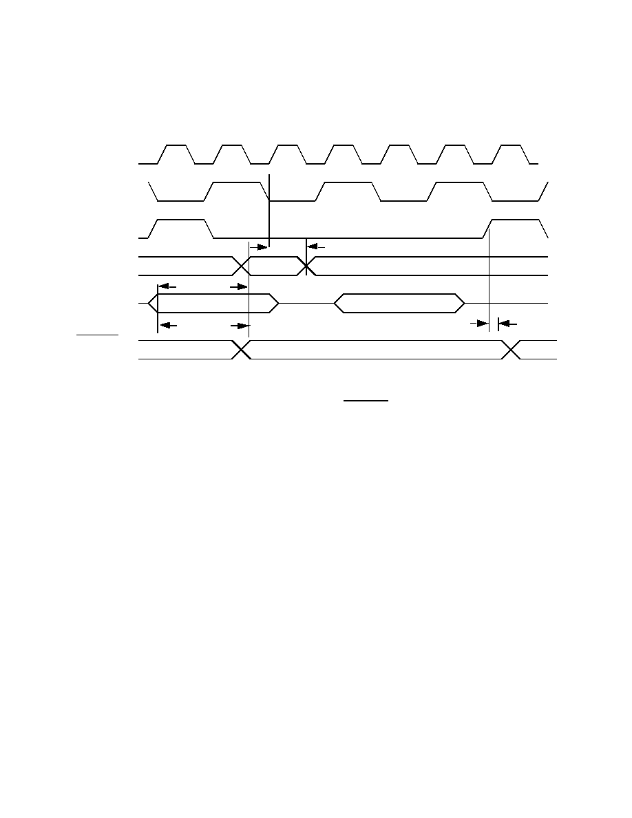
5.0 AC CHARACTERISTICS READ CYCLE
(V
DD
= 5.0V
�
10%) (T
C
= -55
�
C to +125
�
C for "C" screening and -40
�
C to +125
�
C for "W" screening)
SYMBOL
PARAMETER
MINIMUM
MAXIMUM
UNIT
t
AVYV
5
Address VALID to READY setup
2T
OSC
- 30
ns
t
YLYH
5
Non-READY time
No upper limit
ns
t
CLYX
1,5
READY hold after CLKOUT low
0
2T
OSC
- 20
ns
t
LLYX
1,5
READY hold after ALE low
T
OSC
3T
OSC
- 20
ns
t
AVGV
5
Address valid to BUSWIDTH setup
2T
OSC
- 30
ns
t
CLGX
5
BUSWIDTH hold after CLKOUT low
0
ns
t
AVDV
2,5
Address valid to input data valid
3T
OSC
- 29
ns
t
RLDV
2
RD Active to input data valid
5 (see Note 5)
T
OSC
- 26
ns
t
CLDV
5
CLKOUT low to input data valid
5
T
OSC
- 26
ns
t
RHDZ
5
End of RD to input data float
0
T
OSC
-10
ns
t
RXDX
5
Data hold after RD inactive
0
T
OSC
-10
ns
f
OSC
5
Frequency on XTAL1
1 (see Note 7)
20 (see Note 6)
Mhz
T
OSC
5
XTAL1 period (1/f
OSC
)
50 (see Note 6)
1000 (see Note 7)
ns
t
XHCH
XTAL1 high to CLKOUT high or low
0
+25
ns
t
CLCL
6
CLKOUT cycle time
2T
OSC
Typical
ns
t
CHCL
5
CLKOUT high period
T
OSC
- 10
T
OSC
+10
ns
t
CLLH
CLKOUT falling edge to ALE rising
-5
+15
ns
t
LLCH
5
ALE falling edge to CLKOUT rising
-10
+10
ns
t
LHLH
2, 6
ALE cycle time
4T
OSC
Typical
ns
t
LHLL
5
ALE high period
T
OSC
- 10
T
OSC
+15
ns
t
AVLL
5
Address setup to ALE falling edge
T
OSC
- 15
ns
t
LLAX
Address hold after ALE falling edge
T
OSC
- 20
T
OSC
+5
ns
t
LLRL
ALE falling edge to RD falling edge
T
OSC
- 5
T
OSC
+10
ns
t
RLCL
RD low to CLKOUT falling edge
-5
+10
ns
t
RLRH
2
RD low period
T
OSC
- 5
ns
t
RHLH
3,5
RD rising edge to ALE rising edge
T
OSC
-10
T
OSC
+10
ns
t
RLAZ
5
RD low to address float
-5
+5
ns
27
Note:
* Post-radiation performance guaranteed at 25
�
C per MIL-STD-883 Method 1019 at 1.0E5 rads(Si).
1. If max exceeded, additional wait state occurs.
2. If wait states are used, add 2 T
OSC
*N, where N = number of wait states.
3. Assuming back-to-back bus cycles.
4. 8-bit only
5. Tested only at initial qualification, and after any design or process changes which may affect this characteristic.
6. These specs are verified using functional vectors (strobed) only.
7. Low speed tests performed at 5MHz. 1MHz operation is guaranteed by design.
t
LLWL
5
ALE falling edge to WR falling edge
T
OSC
- 10
T
OSC
+10
ns
t
CLWL
CLKOUT low to WR falling edge
-5
+10
ns
t
QVWH
2
Data stable to WR rising edge
T
OSC
- 10
T
OSC
+10
ns
t
CHWH
5
CLKOUT high to WR rising edge
-10
+15
ns
t
WLWH
2,5
WR low period
T
OSC
- 10
ns
t
WHQX
5
Data hold after WR rising edge
T
OSC
- 10
T
OSC
+10
ns
t
WHLH
3,5
WR rising edge to ALE rising edge
T
OSC
- 10
T
OSC
+10
ns
t
WHBX
5
BHE, INST after WR rising edge
T
OSC
- 10
T
OSC
+10
ns
t
WHAX
4,5
AD8-15 HOLD after WR rising
T
OSC
- 25
ns
t
RHBX
5
BHE, INST after RD rising edge
T
OSC
- 10
T
OSC
+10
ns
t
RHAX
4,5
AD8-15 HOLD after RD rising
T
OSC
- 25
ns
t
AVENV
5
Address valid to EDACEN valid
2T
OSC
-30
ns
t
LHENX
5
EDACEN hold after ALE high
0
ns
t
AVEV
2,5
Address valid to EDAC input valid
3T
OSC
-29
ns
t
RXEX
5
EDAC hold after RD inactive
0
T
OSC
-10
ns
t
EVWH
2,5
EDAC output stable to WR rising
T
OSC
-10
T
OSC
+10
ns
t
WHEX
5
EDAC output hold after WR rising
T
OSC
-10
T
OSC
+10
ns

28
XTAL1
CLKOUT
READ
BUS
WRITE
BUS
BHE, INST
AD8-15
t
LLCH
t
CLCL
t
XHCH
t
CHCL
t
RLCL
ALE
t
LHLH
t
LHLL
t
LLRL
t
RHLH
t
RLRH
t
RLDV
t
LLAX
t
AVLL
t
RLAZ
t
RHDZ
T
OSC
Figure 4. System Bus Timings
ADDRESS OUT
DATA
t
AVDV
t
LLWL
t
WLWH
t
WHLH
t
WHQX
t
QVWH
ADDRESS OUT
DATA OUT
ADDRESS
ADDRESS OUT
VALID
t
WHBX,
t
RHBX
t
CLDV
t
RXDX
t
CLWL
t
CLLH
t
CHWH
t
WHAX,
t
RHAX
ECB(5:0) READ
CYCLE
ECB(5:0)
WRITE CYCLE
t
AVEV
VALID
t
RXEX
VALID
t
WHEX
t
EVWH

29
XTAL1
CLKOUT
ALE
READY
READ
BUS
WRITE
BUS
ADDRESS OUT
ADDRESS
DATA OUT
ADDRESS
DATA
t
RLRH
+ 2T
OSC
t
WLWH
+2T
OSC
T
OSC
t
CHCL
t
RLDV
+ 2T
OSC
t
AVYV
t
QVWH
+ 2T
OSC
t
AVDV
+ 2T
OSC
t
XHCH
t
CLCL
t
LHLH
+ 2T
OSC
t
CLLH
t
LLYX
max
t
CLYX
max
t
LLYX
min
t
CLYX
min
t
YLYH
Figure 5. READY Timing (One Wait State)
30
Figure 6. BUSWIDTH and EDACEN Timings
CLKOUT
ALE
BUSWIDTH
BUS
t
CLGX
XTAL1
VALID
t
AVGV
ADDRESS OUT
DATA
EDACEN
t
AVENV
VALID
t
LHENX
31
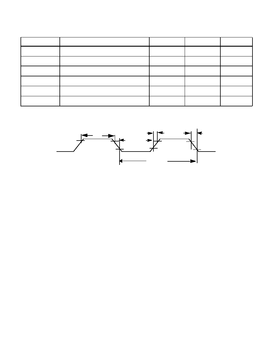
6.0 XTAL1 CLOCK DRIVE TIMING CHARACTERISTICS
Note:
1. Tested only at initial qualification, and after any design or process changes which may affect this characteristic.
2. Supplied as a design limit, but not guaranteed or tested.
Figure 7. External Clock Drive Timing Waveforms
SYMBOL
PARAMETER
MINIMUM
MAXIMUM
UNIT
f
OSC
Oscillator Frequency
1
(note 1)
20
MHz
T
OSC
Oscillator Period
50
1000
(note 1)
ns
t
OSCH
High Time
17
(note 1)
ns
t
OSCL
Low Time
17
(note 1)
ns
t
OSCR
Rise Time
10
(note 2)
ns
t
OSCF
Fall Time
10
(note 2)
ns
t
OSCH
T
OSC
t
OSCF
t
OSCR
0.7 V
D D
0.7 V
DD
0.3V
DD
0.3V
DD
t
OSCL
0.7 V
DD
32
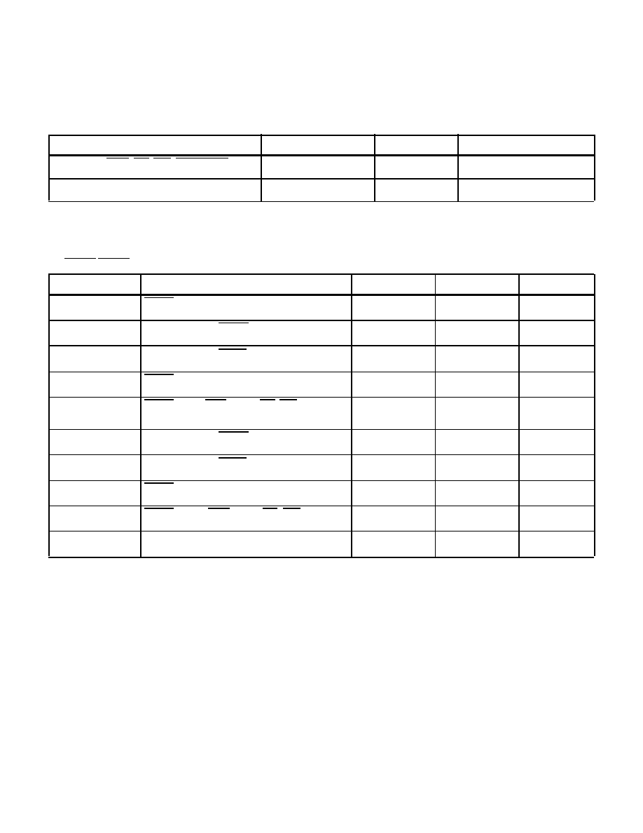
Note:
1.Tested only at initial qualification, and after any design or process changes which may affect this characteristic.
7.0 HOLD/HLDA Timings
Note:
1.Tested only at initial qualification, and after any design or process changes which may affect this characteristic.
Table 11. DC Specifications in Hold
DESCRIPTION
MIN
MAX
CONDITIONS
Pullups on ADV, RD, WR, WRL, BHE, ALE
6.9K
36.7K
V
DD
=5.5V, V
IN
= V
SS
Pulldown on INST
3.7K
27.5K
V
DD
=5.5V, V
IN
= V
DD
SYMBOL
PARAMETER
MINIMUM
MAXIMUM
UNIT
t
HVCH
1
HOLD Setup
25
ns
t
CLHAL
1
CLKOUT low to HLDA low
-15
15
ns
t
CLBRL
1
CLKOUT low to BREQ low
-15
15
ns
t
HALAZ
1
HLDA low to address float
10
ns
t
HALBZ
1
HLDA low to BHE, INST, RD, WR
driven weakly
15
ns
t
CLHAH
1
CLKOUT low to HLDA high
-15
15
ns
t
CLBRH
1
CLKOUT low to BREQ high
-15
15
ns
t
HAHAX
1
HLDA high to address no longer float
-15
ns
t
HAHBV
1
HLDA high to BHE, INST, RD, WR valid
-10
ns
t
CLLH
1
CLKOUT low to ALE high
-5
15
ns

33
CLKOUT
HOLD
HLDA
BREQ
BUS
ALE/ADV
BHE, INST
RD, WR
t
HVCH
t
HVCH
t
CLHAL
t
CLHAH
t
CLBRL
t
CLBRH
t
HAHAX
t
HALAZ
t
HALBZ
t
HAHBV
Weakly Driven Inactive
t
CLLH
Weakly Driven High
Figure 8. DC Specifications In Hold
34
UT80C196KD
XTAL1
External Clock
Input
Figure 9. External Clock Connections
V
DD
0.0V
1.4V
1.4V
TEST POINTS
AC Testing inputs are driven at V
DD
for a Logic "1" and 0.0V for a Logic "0". Timing measure-
ments are made at 1.4V.
Figure 10. AC Testing Input, Output Waveforms
V
LOAD
For timing purposes a port pin is no longer floating when it changes to a voltage outside the ref-
erence points shown and begins to float when it changes to a voltage inside the reference points
shown. I
OL
= 4mA, I
OH
= -4mA.
V
OL
+ 0.5V
V
OH
- 0.5V
V
OL
+ 0.5V
V
OH
- 0.5V
TIMING REFERENCE
POINTS
Figure 11. Float Waveforms
35
Table 12. Serial Port Timing
SYMBOL
PARAMETER
MINIMUM
MAXIMUM
UNIT
t
XLXL
2
Serial port clock period (BRR > 8002H)
6 T
OSC
typical
ns
t
XLXH
1
Serial port clock falling edge to rising edge
(BRR > 8002H)
4 T
OSC
-50
4 T
OSC
+50
ns
t
XLXL
2
Serial port clock period (BRR = 8001H)
4 T
OSC
typical
ns
t
XLXH
1
Serial port clock falling edge to rising edge
(BRR = 8001H)
2 T
OSC
-50
2 T
OSC
+50
ns
t
QVXH
1
Output data valid to clock rising edge
2 T
OSC
-50
ns
t
XHQX
1
Output data hold after clock rising edge
2 T
OSC
-50
ns
t
XHQV
1
Next output data valid after clock rising edge
2 T
OSC
+50
ns
t
DVXH
1
Input data setup to clock rising edge
T
OSC
+50
ns
t
XHDX
1
Input data hold after clock rising edge
0
ns
t
XHQZ
1
Last clock rising to output float
2 T
OSC
-10
2 T
OSC
+10
ns
TXD
RXD (OUT)
RXD (IN)
0
1
2
3
4
5
6
7
T
XLXL
t
QVXH
t
XHQV
t
XHQX
t
DVXH
t
XHDX
t
XLXH
t
XHQZ
Figure 12. Serial Port Waveform - Shift Register Mode
0
1
2
3
5
4
6
7
6
Note :
1. Tested only at initial qualification, and after my design or process changes which may affect this characteristic.
2. These specs are verified functional vectors (strobed) only.

36
APPENDIX A
Difference Between Industry Standard and UT80C196KD
1.0 UT80C196KD DIFFERENCES TO INDUSTRY
STANDARD 80C196KD
1.1 Analog to Digital Converter
The Analog to Digital Converter will not be implemented in the
UT80C196KD.
1.3 Clocking
The XTAL2 output is not used and the UT80C196KD expects
the input on the XTAL 1 to be a valid digital clock signal. The
clock should be stable before reset is removed or Power Down
mode is exited. In Power Down mode, a small number of gates
will be clocked by the XTAL1 input. The UT80C196KD will
drive XTAL2 low when not in test mode.
1.4 CCB Read after Reset
The CCB fetch after Reset will be a normal fetch as if the chosen
bus width is selectable based on the BUSWIDTH input. Systems
with an 8-bit wide interface should tie BUSWIDTH to ground.
Systems that use BUSWIDTH should perform a normal decode
based on the memory configuration of the system. The Industry
Standard 80C196KD treats the CCB fetch as an 8-bit fetch
(driving the upper 8-bits with address 20H) regardless of the
state of BUSWIDTH.
1.5 Internal Program Memory
The UT80C196KD does not have internal program memory,
and pin 2 (EA) will be ignored for choosing between internal
and external program reads. The user may tie this pin to ground
for compatibility reasons, unless EDAC is enabled.
1.6 Ports 3 and 4
Since the UT80C196KD will not have internal program
memory, Ports 3 and 4 will always be used as the multiplexed
Address and Data bus. Therefore, these ports will not be
configured as I/O ports, and the bidirectional port function of
these pins will not be implemented. The pins will only be
configured as Address and bidirectional data pins.
1.7 Built in EDAC
The UT80C196KD incorporates a built in Error Detection and
Correction circuit for external memory reads and writes. The
EDAC can be controlled from an external pin. The external pin
(Pin 37) can be used to enable or disable this feature
interactively. Therefore, different regions of external memory
can be assigned to have EDAC as necessary. Additionally, the
EDAC check bits will be passed through Port 0, which varies
from the industry standard version where Port 0 is an input only
port. You can control the interrupt behavior of the EDAC engine
by setting bits 6 and 5 of the EDAC Control and Status Register
(EDAC_CS). Additionally, reading bit 4 of the EDAC_CS
allows you to determine if a double bit error occurred, and
reading bits 3 through 0 of the EDAC_CS Register tells you
how many single bit errors have been corrected. The EDAC_CS
Register is located at location 15h of HWindow 1.
1.8 Instruction Queue
The instruction queue is eight bytes deep instead of four. The
instruction queue also interfaces to the CPU through a 16-bit
bus. This configuration will speed up the operation of the
UT80C196KD.
1.9 WDT and Prescalar
The WDT can now be disabled through the software. The disable
feature should allow the user flexibility in using the Watch Dog
Timer. The WDT also now has a prescalar which can slow down
the counter by a factor of 2
0
to 2
7
. The prescalar will give the
user extra time between clears of the WDT. The WDT prescaler
(WDT_SCALE) is located at location 0Dh of HWindow 1.
1.10 Interrupt Priority Levels
An additional level of priority encoding is available to the user.
Every standard interrupt can be programed to a higher level of
priority. All interrupts in the higher priority will maintain their
relative priority, but low priority interrupts can then be
programmed for a higher interrupt priority if necessary. The
interrupt priority register is 16-bits wide, and maps to the
standard interrupts in the same fashion as the INT_MASK and
INT_MASK1 registers. The high byte of the Interrupt Priority
Register (IN_PRI(hi)) is located at 0Bh of HWindow 1, and the
low byte (INT_PRI(lo)) is located at 0Ah of HWindow 1.
1.11 Faster Multiply and Divide
The multiplier and divider have been optimized to perform their
operations in fewer state times than in the current version.
1.12 Instructions State Time Reduction
The CPU has been streamlined for faster execution where
possible. Examples include 1 state reduction for WORD
immediate instructions, 1 state reductions for long indexed
instructions, and state reductions for the BMOV instructions.
1.13 STACK_PNTR implemented as Special Function
Register
The STACK_PNTR has been implemented as a true Special
Function Register instead of in the RAM to allow for quicker
pushes and pops. If the stack is not used, the SFR can be used
for general purpose data storage.
1.14 Timer3
An additional 16-bit timer/counter has been implemented as a
general purpose timer that can be used if Timer1 and Timer 2
are being dedicated to other functional uses. The current value
37
of Timer3 can be found in locations 0Fh (high byte), and 0Eh
(low byte) of HWindow 1.
1.15 Input/Output Pullup/Pulldown Currents
Leakage currents may not meet the industry standard
80C196KD specs due to differently sized weak pullups/
pulldowns, during Quasi-Bidirectional and reset/powerdown
modes. Refer to specs for I
LI1
and I
LI2
.
1.16 Power-down exit
Pin 37 will not be used to exit power-down mode. Since a digital
clock is supplied, no connection between this V
pp
pin and the
power-down circuitry exists.
1.17 Test Mode Entry
Test mode entry will be via four pins: WR, RD, ALE and HLDA
instead of PWM0.
1.18 Power-on Reset
The UT80C196KD will not guarantee the 16-state "pulse
stretching" function of a Reset_n pulse applied at power-up. The
user must hold Reset_n low until the power and clocks stabilize
plus 16-state times, or provide a high to low transition after the
power and clocks have stabilized.
1.19 Pullup/Pulldown states
The INST pin will be driven to a weak low during Reset. The
ALE signal will be driven to a weak high during Bus Hold.
1.20 Modifying the INT_PEND registers
Two operand rd-modify-wr instructions should be used to
modify the INT_PEND registers. Three operand rd-modify-wr
instructions may lose an incoming interrupt.
1.21 Serial Port Synchronous Mode
The last clock rising edge to output float time (T
XHQZ
) is made
consistent with the output data hold (T
XHQX
) time of 2 T
OSC
+/-50nsec. This is longer than the industry standard of 1 T
OSC
max.
1.22 Industry Standard Register Indirect with Auto Incre-
ment
The industry standard 80C196KD increments the auto-incre-
mented register after determining the external address instead
of at the end of the instruction completion. The UT80C196KD
performs the auto-increment function at the end of the instruc-
tion processing. Please reference the example below that
shows the processing difference between the UT80C196KD
and the industry standard 80C196KD:
ST R0, [R0]+
assume R0 holds the value 1000h before the instruction is exe-
cuted.
1.23 AC Timing Differences
There are some AC timing differences between the
UT80C196KD and the industry standard 80C196KD. Most
changes resulted in loosened timing specifications. However,
the t
RHDZ
and t
RXDX
timing specifications were tightened by
5ns. If you have been designing to the industry standard
80C196KD timing specifications, it is important to recognize
these two shortened timing specifications.
NOTE: Please visit the UTMC website at www.utmc.com to
obtain the latest data sheet updates, application notes, software
examples, advisories and erratas for the UT80C196KD.
1.24 T2UP-DN Input Signal
Port 2.6 has an alternate function of T2UP-DN enabled by
IOC2.1. The industry standard device appears to allow writes
into Port 2.6 to directly affect the pin state when in the T2UP-
DN mode. (This would allow software control of the T2 direc-
tion, but requires ensuring a one (QBD pullup) is written to
Port 2.6 if the pin is driven externally). The UT80C196KD
device is designed to disable the Port 2.6 output when T2UP-
DN is enabled. This protects the P2.6/T2UP-DN pin from con-
tention with an externally driven signal, independent of the
value written into Port 2.
1.25 NEG 8000h Instruction Operation
The UT80CRH196KD and the industry standard 80C196KD
set the N-Flag differently when executing the NEG 8000h
instruction. NEG represents the MCS-96 opcode to negate a
defined operand (8000h). When the UT80CRH196KD exe-
cutes the NEG 8000h instruction, the result becomes 8000h
with both the N-Flag and the V-Flag set. The industry stan-
dard 80C196KD, however, executes the NEG 8000h instruc-
tion with a result of 8000h and only the V-Flag set.
PROCESSING FLOW FOR THE ST R0, [R0]+
INSTRUCTION
UT80C196KD
Industry Standard
80C196KD
Address = [R0]; 1000h
Address = [R0]; 1000h
R0 ---> Address
R0 = R0+1; 1001h
R0 = R0+1; 1001h
R0 ---> Address
* The contents in address
1000h are 1000h
* The contents in address
1000h are 1001h

38
1.26 Reserved Opcode EEH
The industry standard 80C196KD using the MCS-96 ISA
declares the opcode EEH as a reserved opcode and does not
guarantee the generation of the Unimplemented Opcode Inter-
rupt. The UT80CRH196KD, on the other hand, generates the
Unimplemented Opcode Interrupt when the EEH opcode is
executed.
1.27 Byte-Wide Reads of the HSI_Time SFR
In order to ensure that the next HSI event is loaded from the
FIFO into the HSI holding register, the HSI_TIME special
function register must be read as a 16-bit word. Byte-wide
reads of the HSI_TIME register will not result in successful
loading of the HSI holding register.
1.28 BMOV and BMOVI Maximum Count Limitation
The BMOV and BMOVI instructions provide a powerful
method to transferring a large block of data from one location
in memory to another. The syntax for the BMOV and BMOVI
instructions are as follows:
BMOV
SRC_DEST_REG, CNTREG
BMOVI
SRC_DEST_REG, CNTREG
The SRC_DEST_REG is a long register that contains both
addresses for the source and destination blocks. The CNTREG
is a 16-bit register specifying the number of transfers being
performed. Unlike the industry standard 80C196KD which
will accept any 16-bit counter value, the UT80C196KD will
only accept a value in the range of 0000H to 3FFFH.
1.29 BREQ Activation Prior to HLDA
The BREQ signal is used by the UT80C196KD to signal a
DMA arbiter that it would like to recover access to the mem-
ory bus. The UT80C196KD, on the other hand, uses the
HLDA signal to provide confirmation to the DMA arbiter that
the UT80C196KD has relinquished control of the memory
bus. If the wait state control signal (READY) is high when the
UT80C196KD decides it will release the bus based on the
assertion of the HOLD signal, it will drive the BREQ low one
CLKOUT cycle ahead of its assertion of the HLDA. Con-
versely, if the READY signal is low when the UT80C196KD
decides to relinquish the bus, it will assert BREQ coincidently
with HLDA or some CLKOUT cycle later. The latter behavior
is compatible with the industry standard 80C196KD function-
ality, but the former is unique to the UT80C196KD.
1.30 HOLD Must Be Synchronized with CLKOUT
The DMA arbiter must synchronize the HOLD signal with the
CLKOUT on the UT80C196KD. The timing diagram in Fig-
ure 8 eludes to the synchronicity of the HOLD signal, but does
not clearly identify the outcome if the HOLD signal does not
satisfy the timing parameter t
HVCH
. If the HOLD setup time is
violated on the industry standard 80C196KD, it will require
one additional CLKOUT cycle before it recognizes the state
change of HOLD. Violating the HOLD setup time on the
UT80C196KD will result in a metastable condition and the
UT80C196KD's reaction is undefined.
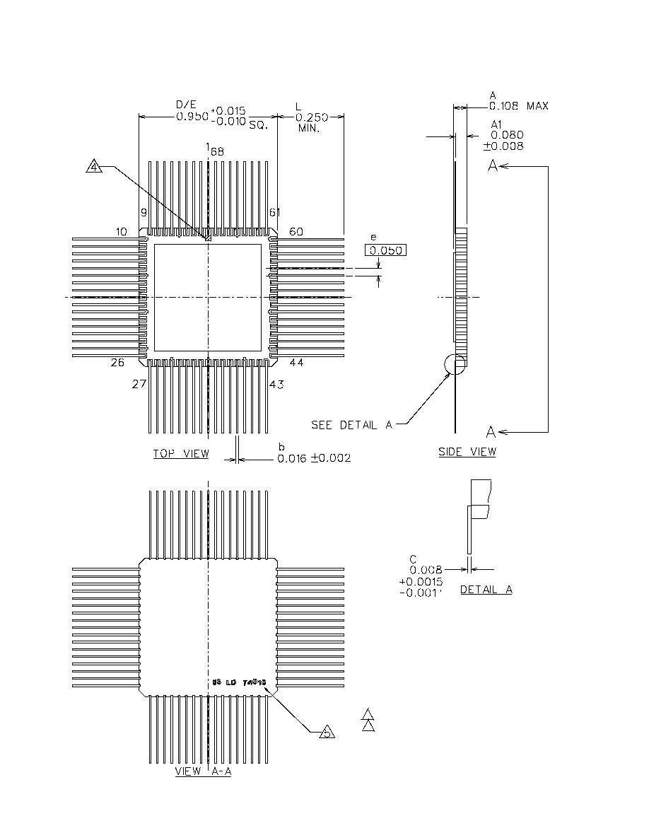
39
8.0 PACKAGE
Notes:
1. All package finishes are per MIL-PRF-38535.
2. Letter designations are for cross-reference to MIL-STD-1835.
3. All leads increase max. limit by 0.003 measured at the
center of the flat, when lead finish A (solder) is applied.
4. ID mark: Configuration is optional.
5. Lettering is not subject to marking criteria.
6. Total weight is approx. 8.0 grams.
Figure 12. 68-lead Quad Flatpack

40
ORDERING INFORMATION
UT80C196KD 16-Bit Microcontroller: SMD
Lead Finish: (Note 1, 2)
(A) = Solder
(C) = Gold
(X) = Optional
Case Outline:
(X) = 68-lead top brazed flatpack
Class Designator:
(Q) = Class Q
Device Type
(01) = 20 Mhz, 16-bit microcontroller
(02) = 20 Mhz, 16-bit microcontroller, Extended Industrial Temp (-40
o
C to +125
o
C)
Drawing Number: 98583
Total Dose:
None
Federal Stock Class Designator: No options
5962 - 98583 01 * * *
Notes:
1. Lead finish (A, C, or X) must be specified.
2. If an "X" is specified when ordering, part number will match the lead finish and will be either "A" (solder) or "C" (gold).

41
UT80C196KD Microcontroller
UT80C196KD - * * *
Lead Finish: (Note 1, 2)
(A) = Solder
(C) = Gold
(X) = Optional
Screening: (Note 3, 4, 5)
(C) = Mil Temp
(P) = Prototype
(W) = Extended Industrial Temp (-40
o
C to +125
o
C)
Package Type:
(W) = 68-lead top brazed Flatpack
UTMC Core Part Number
Notes:
1. Lead finish (A,C, or X) must be specified.
2. If an "X" is specified when ordering, then the part number will match the lead finish and will be either "A" (solder) or "C" (gold).
3. Military Temperature Range flow per UTMC Manufacturing Flows Document. Devices are tested -55C, room temp, and 125C.
4. Prototype flow per UTMC Manufacturing Flows Document Tested at 25C only. Lead finish is gold only.
5. Extended Industrial Temperature Range Flow per UTMC Manufacturing Flows Document. Devices are tested at -40
o
C, room temp, and +125
o
C.
Radiation is neither tested nor guaranteed.

42
Notes