
1
FEATURES
17ns maximum access time
Asynchronous operation for compatibility with industry-
standard 512K x 8 SRAMs
CMOS compatible inputs and output levels, three-state
bidirectional data bus
- I/O Voltage 3.3 volts, 1.8 volt core
Radiation performance
- Intrinsic total-dose: 300 Krad(Si)
- SEL Immune >100 MeV-cm
2
/mg
- LET
th
(0.25): 53.0 MeV-cm
2
/mg
- Memory Cell Saturated Cross Section 1.67E-7cm
2
/bit
- Neutron Fluence: 3.0E14n/cm
2
- Dose Rate
- Upset 1.0E9 rad(Si)/sec
- Latchup 1.0E11 rad(Si)/sec
Packaging options:
- 68-lead ceramic quad flatpack (20.238 grams with lead
frame)
Standard Microcircuit Drawing 5962-04227
- QML compliant part
INTRODUCTION
The UT8CR512K32 is a high-performance CMOS static RAM
multi-chip module (MCM), organized as four individual
524,288 words by 8 bit SRAMs with common output enable.
Easy memory expansion is provided by active LOW chip
enables (EN), an active LOW output enable (G), and three-state
drivers. This device has a power-down feature that reduces
power consumption by more than 90% when deselected.
Writing to each memory is accomplished by taking the
corresponding chip enable (En) input LOW and write enable
(Wn) input LOW. Data on the I/O pins is then written into the
location specified on the address pins (A
0
through A
18
). Reading
from the device is accomplished by taking the chip enable (En)
and output enable (G) LOW while forcing write enable (Wn)
HIGH. Under these conditions, the contents of the memory
location specified by the address pins will appear on the I/O pins.
The input/output pins are placed in a high impedance state when
the device is deselected (En HIGH), the outputs are disabled (G
HIGH), or during a write operation (En LOW and Wn LOW).
Perform 8, 16, 24 or 32 bit accesses by making Wn along with
En a common input to any combination of the discrete memory
die.
Standard Products
UT8CR512K32 16 Megabit SRAM
Advanced Data Sheet
October 2004
www.aeroflex.com/4MSRAM
Figure 1. UT8CR512K32 SRAM Block Diagram
512K x 8
512K x 8
512K x 8
512K x 8
DQ(31:24)
or
DQ3(7:0)
DQ(23:16)
or
DQ2(7:0)
DQ(15:8)
or
DQ1(7:0)
DQ(7:0)
or
DQ0(7:0)
G
A(18:0)
W3
E3
E2
E1
E0
W2
W1
W0
2
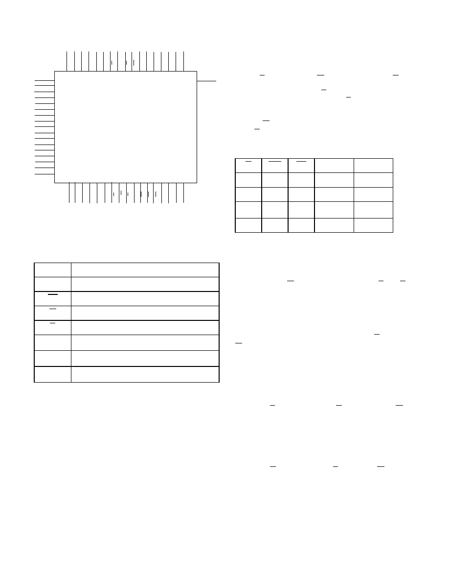
PIN NAMES
DEVICE OPERATION
Each die in the UT8CR512K32 has three control inputs called
Enable (En), Write Enable (Wn), and Output Enable (G); 19
address inputs, A(18:0); and eight bidirectional data lines,
DQ(7:0). The device enable (En) controls device selection,
active, and standby modes. Asserting En enables the device,
causes I
DD
to rise to its active value, and decodes the 19 address
inputs to each memory die by selecting the 2,048,000 byte of
memory. Wn controls read and write operations. During a read
cycle, G must be asserted to enable the outputs.
Table 1. Device Operation Truth Table
Notes:
1. "X" is defined as a "don't care" condition.
2. Device active; outputs disabled.
READ CYCLE
A combination of Wn greater than V
IH
(min) with En and G less
than V
IL
(max) defines a read cycle. Read access time is
measured from the latter of device enable, output enable, or valid
address to valid data output.
SRAM read Cycle 1, the Address Access is initiated by a change
in address inputs while the chip is enabled with G asserted and
Wn deasserted. Valid data appears on data outputs DQn(7:0)
after the specified t
AVQV
is satisfied. Outputs remain active
throughout the entire cycle. As long as device enable and output
enable are active, the address inputs may change at a rate equal
to the minimum read cycle time (t
AVAV
).
SRAM read Cycle 2, the Chip Enable-controlled Access is
initiated by En going active while G remains asserted, Wn
remains deasserted, and the addresses remain stable for the
entire cycle. After the specified t
ETQV
is satisfied, the eight-bit
word addressed by A(18:0) is accessed and appears at the data
outputs DQn(7:0).
SRAM read Cycle 3, the Output Enable-controlled Access is
initiated by G going active while En is asserted, Wn is
deasserted, and the addresses are stable. Read access time is
t
GLQV
unless t
AVQV
or t
ETQV
have not been satisfied.
A(18:0)
Address
DQ(7:0)
Data Input/Output
EN
Enable
W
Write Enable
G
Output Enable
V
DD1
Power (1.8V)
V
DD2
Power (3.3V)
V
SS
Ground
1
2
3
4
5
6
7
8
9
10
11
12
13
14
15
16
17
51
50
49
48
47
46
45
44
43
42
41
40
39
38
37
36
35
68 67 66 65 64 63 62 61 60 59 58 57 56 555453 52
1819 20 21 22 23 24 25 26 27 28 29 30 31 32 33 34
Top View
DQ0(0)
DQ1(0)
DQ2(0)
DQ3(0)
DQ4(0)
DQ5(0)
DQ6(0)
DQ7(0)
V
SS
DQ0(1)
DQ1(1)
DQ2(1)
DQ3(1)
DQ4(1)
DQ5(1)
DQ6(1)
DQ7(1)
DQ0(2)
DQ1(2)
DQ2(2)
DQ3(2)
DQ4(2)
DQ5(2)
DQ6(2)
DQ7(2)
V
SS
DQ0(3)
DQ1(3)
DQ2(3)
DQ3(3)
DQ4(3)
DQ5(3)
DQ6(3)
DQ7(3)
V
DD1
A0
A1
A2
A3
A4
A5
E
2
V
SS
E
3
W
0
A6
A7
A8
A9
A10
V
DD2
V
DD2
A1
1
A1
2
A1
3
A1
4
A1
5
A1
6
E
0
G
E
1
A1
7
W
1
W
2
W
3
A1
8
V
DD1
V
SS
G
WN
EN
I/O Mode
Mode
X
X
1
3-state
Standby
X
0
0
Data in
Write
1
1
0
3-state
Read
2
0
1
0
Data out
Read
Figure 2. 17ns SRAM Pinout 68)
3
WRITE CYCLE
A combination of Wn less than V
IL
(max) and En less than
V
IL
(max) defines a write cycle. The state of G is a "don't care"
for a write cycle. The outputs are placed in the high-impedance
state when either G is greater than V
IH
(min), or when Wn is less
than V
IL
(max).
Write Cycle 1, the Write Enable-controlled Access is defined
by a write terminated by Wn going high, with En still active.
The write pulse width is defined by t
WLWH
when the write is
initiated by Wn, and by t
ETWH
when the write is initiated by En.
Unless the outputs have been previously placed in the high-
impedance state by G, the user must wait t
WLQZ
before applying
data to the eight bidirectional pins DQn(7:0) to avoid bus
contention.
Write Cycle 2, the Chip Enable-controlled Access is defined by
a write terminated by the former of En or Wn going inactive.
The write pulse width is defined by t
WLEF
when the write is
initiated by Wn, and by t
ETEF
when the write is initiated by the
En going active. For the Wn initiated write, unless the outputs
have been previously placed in the high-impedance state by G,
the user must wait t
WLQZ
before applying data to the eight
bidirectional pins DQn (7:0) to avoid bus contention.
RADIATION HARDNESS
The UT8CR512K32 SRAM incorporates special design and
layout features which allows operation in a limited radiation
environment.
Table 2. Radiation Hardness
Design Specifications
1
Notes:
1. The SRAM is immune to latchup to particles >100MeV-cm
2
/mg.
2. 10% worst case particle environment, Geosynchronous orbit, 100 mils of
Aluminum.
Supply Sequencing
No supply voltage sequencing is required between V
DD1
and
V
DD2
.
Total Dose
300K
rad(Si)
Heavy Ion
Error Rate
2
8.9x10
-10
Errors/Bit-Day

4
ABSOLUTE MAXIMUM RATINGS
1
(Referenced to V
SS
)
Notes:
1. Stresses outside the listed absolute maximum ratings may cause permanent damage to the device. This is a stress rating only, and functional operation of the device at
these or any other conditions beyond limits indicated in the operational sections of this specification is not recommended. Exposure to absolute maximum rating
conditions for extended periods may affect device reliability and performance.
2. Maximum junction temperature may be increased to +175
�C during burn-in and steady-static life.
3. Test per MIL-STD-883, Method 1012.
RECOMMENDED OPERATING CONDITIONS
SYMBOL
PARAMETER
LIMITS
V
DD1
DC supply voltage
-0.3 to 2.0V
V
DD2
DC supply voltage
-0.3 to 3.8V
V
I/O
Voltage on any pin
-0.3 to 3.8V
T
STG
Storage temperature
-65 to +150
�C
P
D
Maximum power dissipation
1.2W
T
J
Maximum junction temperature
2
+150
�C
JC
Thermal resistance, junction-to-case
3
5
�C/W
I
I
DC input current
�
5 mA
SYMBOL
PARAMETER
LIMITS
V
DD1
Positive supply voltage
1.7 to 1.9V
V
DD2
Positive supply voltage
3.0 to 3.6V
T
C
Case temperature range
(C) Screening: -55 to +125
�C
(W) Screening: -40 to +125
�C
V
IN
DC input voltage
0V to V
DD2
5
DC ELECTRICAL CHARACTERISTICS (Pre and Post-Radiation)*
(-55
�C to +125�C for (C) screening and -40�C to 125�C for (W) screening)
Notes:
* Post-radiation performance guaranteed at 25
�C per MIL-STD-883 Method 1019 at 1.0E5 rad(Si).
1. Measured only for initial qualification and after process or design changes that could affect input/output capacitance.
2. Supplied as a design limit but not guaranteed or tested.
3. Not more than one output may be shorted at a time for maximum duration of one second.
4. V
IH
= V
DD2
(max), V
IL
= 0V.
SYMBOL
PARAMETER
CONDITION
MIN
MAX
UNIT
V
IH
High-level input voltage
.7*V
DD2
V
V
IL
Low-level input voltage
.3*V
DD2
V
V
OL1
Low-level output voltage
I
OL
= 8mA,V
DD2
=V
DD2
(min)
.2*V
DD2
V
V
OH1
High-level output voltage
I
OH
= -4mA,V
DD2
=V
DD2
(min)
.8*V
DD2
V
C
IN
1
Input capacitance
= 1MHz @ 0V
12
pF
C
IO
1
Bidirectional I/O capacitance
= 1MHz @ 0V
12
pF
I
IN
Input leakage current
V
IN
= V
DD2
and V
SS
-2
2
�A
I
OZ
Three-state output leakage
current
V
O
= V
DD2
and V
SS,
V
DD2
= V
DD2
(max)
G = V
DD2
(max)
-2
2
�A
I
OS
2, 3
Short-circuit output current
V
DD2
= V
DD2
(max), V
O
= V
DD2
V
DD2
= V
DD2
(max), V
O
= V
SS
-100
+100
mA
I
DD1
(OP
1
) Supply current operating
@ 1MHz
Inputs : V
IL
= V
SS
+ 0.2V
V
IH
= V
DD2
- 0.2V, I
OUT
= 0
V
DD1
= V
DD1
(max), V
DD2
= V
DD2
(max)
45
mA
I
DD1
(OP
2
) Supply current operating
@66MHz
Inputs : V
IL
= V
SS
+ 0.2V,
V
IH
= V
DD2
- 0.2V, I
OUT
= 0
V
DD1
= V
DD1
(max), V
DD2
= V
DD2
(max)
93
mA
I
DD2
(OP
1
) Supply current operating
@ 1MHz
Inputs : V
IL
= V
SS
+ 0.2V
V
IH
= V
DD2
- 0.2V, I
OUT
= 0
V
DD1
= V
DD1
(max), V
DD2
= V
DD2
(max)
243
�A
I
DD2
(OP
2
) Supply current operating
@66MHz
Inputs : V
IL
= V
SS
+ 0.2V,
V
IH
= V
DD2
- 0.2V, I
OUT
= 0
V
DD1
= V
DD1
(max), V
DD2
= V
DD2
(max)
12
mA
I
DD1
(SB)
4
I
DD2
(SB)
4
Supply current standby @
0Hz
CMOS inputs , I
OUT
= 0
EN = V
DD2
-0.2
V
DD1
= V
DD1
(max), V
DD2
= V
DD2
(max)
38
100
m
�A
I
DD1
(SB)
4
I
DD2
(SB)
4
Supply current standby
A(18:0) @ 66MHz
CMOS inputs , I
OUT
= 0
EN = V
DD2
- 0.2
V
DD1
= V
DD1
(max), V
DD2
= V
DD2
(max)
38
100
m
�A

6
AC CHARACTERISTICS READ CYCLE (Pre and Post-Radiation)*
(-55
�C to +125�C for (C) screening and -40�C to +125�C for (W) screening, V
DD1
= V
DD1
(min), V
DD2
= V
DD2
(min))
Notes:
* Post-radiation performance guaranteed at 25
�C per MIL-STD-883 Method 1019.
1. Guaranteed, but not tested.
2. Three-state is defined as a 200mV change from steady-state output voltage.
3. The ET (enable true) notation refers to the latter falling edge of EN. SEU immunity does not affect the read parameters.
4. The EF (enable false) notation refers to the latter rising edge of EN. SEU immunity does not affect the read parameters.
SYMBOL
PARAMETER
8CR512-155
MIN MAX
UNIT
t
AVAV
1
Read cycle time
17
ns
t
AVQV
Read access time
17
ns
t
AXQX
2
Output hold time
3
ns
t
GLQX
1,2
G-controlled output enable time
0
ns
t
GLQV
G-controlled output enable time
7
ns
t
GHQZ
2
G-controlled output three-state time
7
ns
t
ETQX
2,3
E-controlled output enable time
5
ns
t
ETQV
3
E-controlled access time
17
ns
t
EFQZ
4
E-controlled output three-state time
2
7
ns

7
Figure 3c. SRAM Read Cycle 3: Output Enable-Controlled Access
A(18:0)
DQn(7:0)
G
t
GHQZ
Assumptions:
1. En < V
IL
(max) and Wn > V
IH
(min)
t
GLQV
t
GLQX
t
AVQV
DATA VALID
Assumptions:
1. En and G < V
IL
(max) and Wn > V
IH
(min)
A(18:0)
DQn(7:0)
Figure 3a. SRAM Read Cycle 1: Address Access
t
AVAV
t
AVQV
t
AXQX
Previous Valid Data
Valid Data
Assumptions:
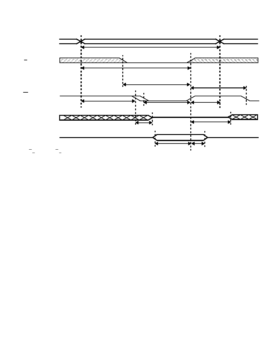
1. G < V
IL
(max) and Wn > V
IH
(min)
A(18:0)
Figure 3b. SRAM Read Cycle 2: Chip Enable-Controlled Access
En
DATA VALID
t
EFQZ
t
ETQX
t
ETQV
DQn(7:0)

8
AC CHARACTERISTICS WRITE CYCLE (Pre and Post-Radiation)*
(-55
�C to +125�C for (C) screening and -40�C to +125�C for (W) screening, V
DD1
= V
DD1
(min), V
DD2
= V
DD2
(min))
Notes:
* Post-radiation performance guaranteed at 25
�C per MIL-STD-883 Method 1019.
1. Test with G high.
2. Three-state is defined as 200mV change from steady-state output voltage.
SYMBOL
PARAMETER
8CR512-15
MIN MAX
UNIT
t
AVAV
1
Write cycle time
17
ns
t
ETWH
Device enable to end of write
12
ns
t
AVET
Address setup time for write (EN- controlled)
0
ns
t
AVWL
Address setup time for write (W - controlled)
0
ns
t
WLWH
Write pulse width
12
ns
t
WHAX
Address hold time for write (W - controlled)
2
ns
t
EFAX
Address hold time for device enable (EN- controlled)
0
ns
t
WLQZ
2
W - controlled three-state time
5
ns
t
WHQX
2
W - controlled output enable time
4
ns
t
ETEF
Device enable pulse width (EN - controlled)
12
ns
t
DVWH
Data setup time
7
ns
t
WHDX
Data hold time
2
ns
t
WLEF
Device enable controlled write pulse width
12
ns
t
DVEF
Data setup time
7
ns
t
EFDX
Data hold time
0
ns
t
AVWH
Address valid to end of write
12
ns
t
WHWL
1
Write disable time
3
ns
9
Assumptions:
1. G < V
IL
(max). If G > V
IH
(min) then Qn(8:0) will be
in three-state for the entire cycle.
Wn
t
AVWL
Figure 4a. SRAM Write Cycle 1: Write Enable - Controlled Access
A(18:0)
Qn(7:0)
En
Dn(7:0)
APPLIED DATA
t
DVWH
t
WHDX
t
ETWH
t
WLWH
t
WHAX
t
WHQX
t
WLQZ
t
AVWH
t
WHWL

10
t
EFDX
Assumptions & Notes:
1. G < V
IL
(max). If G > V
IH
(min) then Qn(7:0) will be in three-state for the entire cycle.
2. Either En scenario above can occur.
A(18:0)
Figure 4b. SRAM Write Cycle 2: Chip Enable - Controlled Access
Wn
En
Dn(7:0)
APPLIED DATA
En
Qn(7:0)
t
WLQZ
t
ETEF
t
WLEF
t
DVEF
t
AVET
t
AVET
t
ETEF
t
EFAX
t
EFAX
or

11
DATA RETENTION CHARACTERISTICS (Pre-Radiation)
3
(V
DD2
= V
DD2
(min), 1 Sec DR Pulse)
Notes:
* Post-radiation performance guaranteed at 25
�C per MIL-STD-883 Method 1019.
1. EN =
V
DD2
all other inputs = V
DD2
or V
SS
2. V
DD2
= 0 volts to V
DD2
(max)
SYMBOL
PARAMETER
MINIMUM MAXIMUM UNIT
V
DR
V
DD1
for data retention
1.0
1.0
--
V
I
DDR
1
Device Type 1
Data retention current
-55
�C
25
�C
125
�C
--
600
600
30
�A
�A
mA
I
DDR
1
Device Type 2
Data retention current
-40
�C
25
�
125
�C
--
600
600
30
�A
�A
mA
t
EFR
1,2
Chip deselect to data retention time
0
0
ns
t
R
1,2
Operation recovery time
t
AVAV
t
AVAV
ns
V
DD1
DATA RETENTION MODE
t
R
1.7V
V
DR
>
1.0V
Figure 5. Low V
DD
Data Retention Waveform
t
EFR
EN
V
DD2
V
IN
<0.3V
DD2
CMOS
V
SS
V
IN
>0.7V
DD2
CMOS
1.7V
Notes:
1. 50pF including scope probe and test socket.
2. Measurement of data output occurs at the low to high or high to low transition mid-point
(i.e., CMOS input = V
DD2
/2).
90%
Figure 6. AC Test Loads and Input Waveforms
Input Pulses
10%
< 2ns
< 2ns
1.4V
188 ohms
50pF
CMOS
0.0V
V
DD2
-0.05V
12
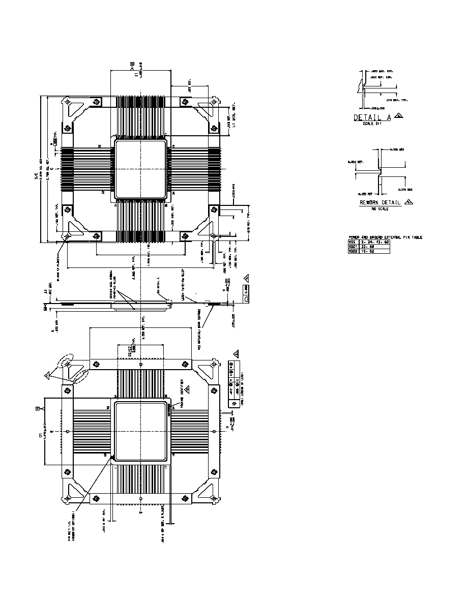
PACKAGING
Figure 7. 68-pin Ceramic FLATPACK
Notes:
1. All exposed metalized areas are gold plated
over electroplated nickel per MIL-PRF-38535.
2. The lid is electrically connected to V
SS
.
3. Lead finishes are in accordance to MIL-PRF-
38535.
4. Ceramic shall be dark alumina.
5. Letter designations are to cross reference to
MIL-STD-1835.
6. Dogleg geometries are optional within
dimensions shown.
7. These areas may have notches and tabs
different than shown.
8. Lead true position tolerances and coplanarity
are not measured.
9. Packages may be shipped with repaired leads
as shown. Coplanarity requirements do not
apply in the repaired area.
10. Numbering and lettering on the ceramic are
not subject to visual or marking criteria.
13
ORDERING INFORMATION
512K32 SRAM:
UT ****
*
- * * * * *
Lead Finish:
(A) = Hot solder dipped
(C) = Gold
(X) = Factory option (gold or solder)
Screening:
(C) = Military Temperature Range flow
(-55
�C to +125�C)
(P) = Prototype flow
(W) = Extended industrial temperature range flow
(-40
�C to +125�C)
Package Type:
(V) =
68-lead ceramic FP
Access Time:
(17) = 17ns access time
Device Type:
(8CR512K32) = 512K x 32SRAM
Notes:
1. Lead finish (A,C, or X) must be specified.
2. If an "X" is specified when ordering, then the part marking will match the lead finish and will be either "A" (solder) or "C" (gold).
3. Prototype flow per UTMC Manufacturing Flows Document. Tested at 25
�
C only. Lead finish is GOLD ONLY. Radiation neither
tested nor guaranteed.
4. Military Temperature Range flow per UTMC Manufacturing Flows Document. Devices are tested at -55
�
C, room temp, and 125
�
C.
Radiation neither tested nor guaranteed.
14
512K x 32 SRAM: SMD
5962 - 04227 ***
**
Lead Finish:
(A) = Hot solder dipped
(C) = Gold
(X) = Factory Option (gold or solder)
Case Outline:
(V) = 68-lead ceramic flatpack
Class Designator:
(Q) = QML Class Q
(V) = QML Class V
Device Type
(01) = 17ns access time, CMOS I/O, 68-lead flatpack package
(-55
�C to +125�C)
(02) = 17ns access time, CMOS I/O, 68-lead flatpack package
(-40
�C to +125�C)
(02TBD)=15ns access time, CMOS I/O, 40-lead flatpack package, dual chip enable (not available)
Drawing Number: 04227
Total Dose:
(R) = 100K rad(Si)
(F) = 300K rad(Si)
Federal Stock Class Designator: No options
* * *
Notes:
1.Lead finish (A,C, or X) must be specified.
2.If an "X" is specified when ordering, part marking will match the lead finish and will be either "A" (solder) or "C" (gold).
3.Total dose radiation must be specified when ordering. QML Q and QML V not available without radiation hardening.

15
NOTES
16
COLORADO
Toll Free: 800-645-8862
Fax: 719-594-8468
SE AND MID-ATLANTIC
Tel: 321-951-4164
Fax: 321-951-4254
INTERNATIONAL
Tel: 805-778-9229
Fax: 805-778-1980
WEST COAST
Tel: 949-362-2260
Fax: 949-362-2266
NORTHEAST
Tel: 603-888-3975
Fax: 603-888-4585
CENTRAL
Tel: 719-594-8017
Fax: 719-594-8468
w w w . a e r o f l e x . c o m i n f o - a m s @ a e r o f l e x . c o m
Our passion for performance is defined by three
attributes represented by these three icons:
solution-minded, performance-driven and customer-focused
Aeroflex UTMC Microelectronic Systems Inc. (Aeroflex)
reserves the right to make changes to any products and
services herein at any time without notice. Consult Aeroflex
or an authorized sales representative to verify that the
information in this data sheet is current before using this
product. Aeroflex does not assume any responsibility or
liability arising out of the application or use of any product
or service described herein, except as expressly agreed to in
writing by Aeroflex; nor does the purchase, lease, or use of a
product or service from Aeroflex convey a license under any
patent rights, copyrights, trademark rights, or any other of the
intellectual rights of Aeroflex or of third parties.